EP0370558A2 - Schreibverfahren mit Schachbrettmustern für eine EEPROM-Speicherzellenmatrix und Gerät zur Durchführung des genannten Verfahrens - Google Patents
Schreibverfahren mit Schachbrettmustern für eine EEPROM-Speicherzellenmatrix und Gerät zur Durchführung des genannten Verfahrens Download PDFInfo
- Publication number
- EP0370558A2 EP0370558A2 EP89202873A EP89202873A EP0370558A2 EP 0370558 A2 EP0370558 A2 EP 0370558A2 EP 89202873 A EP89202873 A EP 89202873A EP 89202873 A EP89202873 A EP 89202873A EP 0370558 A2 EP0370558 A2 EP 0370558A2
- Authority
- EP
- European Patent Office
- Prior art keywords
- writing
- matrix
- impulse
- memory cells
- checkerboard pattern
- Prior art date
- Legal status (The legal status is an assumption and is not a legal conclusion. Google has not performed a legal analysis and makes no representation as to the accuracy of the status listed.)
- Withdrawn
Links
Images
Classifications
-
- G—PHYSICS
- G11—INFORMATION STORAGE
- G11C—STATIC STORES
- G11C29/00—Checking stores for correct operation ; Subsequent repair; Testing stores during standby or offline operation
- G11C29/04—Detection or location of defective memory elements, e.g. cell constructio details, timing of test signals
- G11C29/08—Functional testing, e.g. testing during refresh, power-on self testing [POST] or distributed testing
- G11C29/12—Built-in arrangements for testing, e.g. built-in self testing [BIST] or interconnection details
- G11C29/18—Address generation devices; Devices for accessing memories, e.g. details of addressing circuits
- G11C29/30—Accessing single arrays
- G11C29/34—Accessing multiple bits simultaneously
Definitions
- the present invention relates to a writing process with a checkerboard pattern for a matrix of EEPROM memory cells and a device for executing the above process.
- the checkerboard pattern constituted by a uniform spatial alternation of "0" and "1" written in the bits of a memory matrix, is frequently used during a writing session so as to detect certain types of defects.
- the object of the present invention is to accomplish a writing process for a matrix of EEPROM memory cells which allows the execution of the writing of a checkerboard pattern with a minimum number of writing impulses.
- such object is attained with a writing process characterized in that it includes the use of a first writing impulse to execute the writing of all the cells of a first order of lines (odd or even) and of a second writing impulse to execute the writing of all the cells of a second order of lines (even or odd) of the matrix.
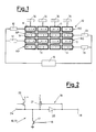
- Fig. 1 there is represented an EEPROM matrix of memory cells 10 divided into bytes 11 each with 4 bits, organized in odd and even lines RD and RP and in columns C.
- the matrix 10 is provided with a writing device consisting essentially of a first plurality of impulse generators or line decoders 12 for the odd lines RD, by a second plurality for the even lines RP, by a third plurality of impulse generators or line decoders 14 for the columns C and by a clock 15 for the alternating activation of the line generators 12 and 13.
- the generators 12 are at first activated together with the column C generators for the simultaneous writing of all the bytes of the odd lines RD of the EEPROM matrix and the generators 13 are then activated together with the column C generators for the simultaneous writing, with alternate bit patterns, of all the bytes of the even lines RP of the same matrix. With just two impulses the writing of the entire memory is thus obtained.
- a possible line generator 12 or 13 is illustrated as an example in Fig. 2 and includes an activation terminal 16 connected to the gate of an N-channel MOS transistor 17, with the source connected to ground and the drain connected to an output terminal 18 by means of a clamping circuit 19 consisting of an amplifier-inverter 20 and a resistive P-channel MOS transistor 21. To these is added a P-channel MOS transistor 22, whose source is connected to a positive power supply and whose drain is connected to an input terminal 24 and whose task it is to pre-load to the same value as the power supply the input terminal 24 through an appropriate command supplied at the gate of transistor 22.
- transistor 17 When a positive signal is applied by the clock 15 to terminal 16, transistor 17 starts to conduct and brings to a low level the input of the clamping circuit 19. The output of the latter thus goes to a high level, so as to order the writing of the bytes of the selected line.
Landscapes
- Read Only Memory (AREA)
- Control Of Indicators Other Than Cathode Ray Tubes (AREA)
Applications Claiming Priority (2)
| Application Number | Priority Date | Filing Date | Title |
|---|---|---|---|
| IT2271788 | 1988-11-24 | ||
| IT8822717A IT1227493B (it) | 1988-11-24 | 1988-11-24 | Procedimento di scrittura con distribuzione a scacchiera per matrice di celle di memoria eprom e dispositivo per l'attuazione del procedimento |
Publications (2)
| Publication Number | Publication Date |
|---|---|
| EP0370558A2 true EP0370558A2 (de) | 1990-05-30 |
| EP0370558A3 EP0370558A3 (de) | 1991-12-27 |
Family
ID=11199603
Family Applications (1)
| Application Number | Title | Priority Date | Filing Date |
|---|---|---|---|
| EP19890202873 Withdrawn EP0370558A3 (de) | 1988-11-24 | 1989-11-13 | Schreibverfahren mit Schachbrettmustern für eine EEPROM-Speicherzellenmatrix und Gerät zur Durchführung des genannten Verfahrens |
Country Status (3)
| Country | Link |
|---|---|
| EP (1) | EP0370558A3 (de) |
| JP (1) | JPH02187995A (de) |
| IT (1) | IT1227493B (de) |
Cited By (1)
| Publication number | Priority date | Publication date | Assignee | Title |
|---|---|---|---|---|
| GB2430522B (en) * | 2004-05-11 | 2008-02-13 | Spansion Llc | Semiconductor device and writing method |
Family Cites Families (2)
| Publication number | Priority date | Publication date | Assignee | Title |
|---|---|---|---|---|
| DE3276399D1 (en) * | 1982-09-22 | 1987-06-25 | Itt Ind Gmbh Deutsche | Electrically programmable memory matrix |
| JP2603205B2 (ja) * | 1987-03-16 | 1997-04-23 | シーメンス、アクチエンゲゼルシヤフト | 多段集積デコーダ装置 |
-
1988
- 1988-11-24 IT IT8822717A patent/IT1227493B/it active
-
1989
- 1989-11-13 EP EP19890202873 patent/EP0370558A3/de not_active Withdrawn
- 1989-11-17 JP JP1297773A patent/JPH02187995A/ja active Pending
Cited By (1)
| Publication number | Priority date | Publication date | Assignee | Title |
|---|---|---|---|---|
| GB2430522B (en) * | 2004-05-11 | 2008-02-13 | Spansion Llc | Semiconductor device and writing method |
Also Published As
| Publication number | Publication date |
|---|---|
| IT1227493B (it) | 1991-04-12 |
| IT8822717A0 (it) | 1988-11-24 |
| EP0370558A3 (de) | 1991-12-27 |
| JPH02187995A (ja) | 1990-07-24 |
Similar Documents
| Publication | Publication Date | Title |
|---|---|---|
| KR100417450B1 (ko) | 연속적으로동작하는디지털메모리의특정라인에대한점프형어드레싱장치 | |
| US4055754A (en) | Memory device and method of testing the same | |
| TW332292B (en) | Method and apparatus for programming memory devices | |
| KR970049545A (ko) | 프로그래머블 패리티 체킹 및 비교 회로 | |
| KR970003252A (ko) | 불휘발성 반도체 메모리의 전압 센싱 방법 | |
| KR950024220A (ko) | 용장 회로 장치 | |
| US3781829A (en) | Test pattern generator | |
| EP0822557A3 (de) | Nichtflüchtige Halbleiterspeicheranordnung mit variabler Source-Spannung | |
| KR870009383A (ko) | 여분의 회로부를 가지는 반도체 메모리 소자 | |
| JP2003204001A5 (de) | ||
| AU583950B2 (en) | Memory system with page mode operation | |
| KR840001731A (ko) | 순차적인 워어드가 정열된 어드레스 지정장치 | |
| JPS63312713A (ja) | タイミング・ジエネレータ | |
| US4244032A (en) | Apparatus for programming a PROM by propagating data words from an address bus to the PROM data terminals | |
| KR102040868B1 (ko) | 반도체 기억 장치 및 그 독출 방법 | |
| JPH07104815B2 (ja) | メモリ | |
| KR970023452A (ko) | 플래쉬 메모리 장치 | |
| EP0370558A2 (de) | Schreibverfahren mit Schachbrettmustern für eine EEPROM-Speicherzellenmatrix und Gerät zur Durchführung des genannten Verfahrens | |
| US4549283A (en) | Digital time delay circuit with high speed and large delay capacity | |
| KR900003884A (ko) | 대규모 반도체 집적회로 장치 | |
| KR870001518A (ko) | 컴퓨터 메모리 장치 | |
| EP0141562B1 (de) | Verfahren und Gerät zur Erzeugung einer Sequenz von Mehrbitworten | |
| US5572198A (en) | Method and apparatus for routing in reduced switch matrices to provide one hundred percent coverage | |
| JPH06215590A (ja) | フラッシュ消去型不揮発性メモリ | |
| ATE209819T1 (de) | Fortgeschrittene programmierverifikation für flash-speicher mit seitenmodus |
Legal Events
| Date | Code | Title | Description |
|---|---|---|---|
| PUAI | Public reference made under article 153(3) epc to a published international application that has entered the european phase |
Free format text: ORIGINAL CODE: 0009012 |
|
| AK | Designated contracting states |
Kind code of ref document: A2 Designated state(s): DE FR GB NL SE |
|
| PUAL | Search report despatched |
Free format text: ORIGINAL CODE: 0009013 |
|
| AK | Designated contracting states |
Kind code of ref document: A3 Designated state(s): DE FR GB NL SE |
|
| STAA | Information on the status of an ep patent application or granted ep patent |
Free format text: STATUS: THE APPLICATION IS DEEMED TO BE WITHDRAWN |
|
| 18D | Application deemed to be withdrawn |
Effective date: 19920531 |