EP0370773B1 - Ansteuerungsverfahren einer mehrschichtigen Flüssigkristall-Anzeigevorrichtung - Google Patents
Ansteuerungsverfahren einer mehrschichtigen Flüssigkristall-Anzeigevorrichtung Download PDFInfo
- Publication number
- EP0370773B1 EP0370773B1 EP89312086A EP89312086A EP0370773B1 EP 0370773 B1 EP0370773 B1 EP 0370773B1 EP 89312086 A EP89312086 A EP 89312086A EP 89312086 A EP89312086 A EP 89312086A EP 0370773 B1 EP0370773 B1 EP 0370773B1
- Authority
- EP
- European Patent Office
- Prior art keywords
- liquid crystal
- cell layer
- voltage
- cell
- birefringence
- Prior art date
- Legal status (The legal status is an assumption and is not a legal conclusion. Google has not performed a legal analysis and makes no representation as to the accuracy of the status listed.)
- Expired - Lifetime
Links
- 239000004973 liquid crystal related substance Substances 0.000 title claims description 209
- 238000000034 method Methods 0.000 title claims description 45
- 210000004027 cell Anatomy 0.000 claims description 109
- 239000000758 substrate Substances 0.000 claims description 20
- 210000002858 crystal cell Anatomy 0.000 claims description 17
- 230000010287 polarization Effects 0.000 claims description 7
- 239000000463 material Substances 0.000 claims description 5
- 230000000694 effects Effects 0.000 claims description 3
- 238000001914 filtration Methods 0.000 claims 2
- 230000003993 interaction Effects 0.000 claims 2
- 239000010408 film Substances 0.000 description 13
- 238000002834 transmittance Methods 0.000 description 13
- 239000003086 colorant Substances 0.000 description 11
- 239000012528 membrane Substances 0.000 description 6
- 238000002474 experimental method Methods 0.000 description 5
- 239000011149 active material Substances 0.000 description 4
- WCLNGBQPTVENHV-MKQVXYPISA-N cholesteryl nonanoate Chemical compound C([C@@H]12)C[C@]3(C)[C@@H]([C@H](C)CCCC(C)C)CC[C@H]3[C@@H]1CC=C1[C@]2(C)CC[C@H](OC(=O)CCCCCCCC)C1 WCLNGBQPTVENHV-MKQVXYPISA-N 0.000 description 3
- 239000004925 Acrylic resin Substances 0.000 description 2
- 229920000178 Acrylic resin Polymers 0.000 description 2
- 239000004642 Polyimide Substances 0.000 description 2
- VYPSYNLAJGMNEJ-UHFFFAOYSA-N Silicium dioxide Chemical compound O=[Si]=O VYPSYNLAJGMNEJ-UHFFFAOYSA-N 0.000 description 2
- 238000004040 coloring Methods 0.000 description 2
- 239000011521 glass Substances 0.000 description 2
- 238000004519 manufacturing process Methods 0.000 description 2
- 239000011159 matrix material Substances 0.000 description 2
- 239000000203 mixture Substances 0.000 description 2
- 230000003287 optical effect Effects 0.000 description 2
- 229920001721 polyimide Polymers 0.000 description 2
- 238000007789 sealing Methods 0.000 description 2
- CMSGUKVDXXTJDQ-UHFFFAOYSA-N 4-(2-naphthalen-1-ylethylamino)-4-oxobutanoic acid Chemical compound C1=CC=C2C(CCNC(=O)CCC(=O)O)=CC=CC2=C1 CMSGUKVDXXTJDQ-UHFFFAOYSA-N 0.000 description 1
- 239000004988 Nematic liquid crystal Substances 0.000 description 1
- 239000004677 Nylon Substances 0.000 description 1
- 239000004372 Polyvinyl alcohol Substances 0.000 description 1
- 229910052681 coesite Inorganic materials 0.000 description 1
- 150000001875 compounds Chemical class 0.000 description 1
- 238000010276 construction Methods 0.000 description 1
- 229910052906 cristobalite Inorganic materials 0.000 description 1
- 230000001419 dependent effect Effects 0.000 description 1
- 238000010586 diagram Methods 0.000 description 1
- 239000006185 dispersion Substances 0.000 description 1
- 230000001747 exhibiting effect Effects 0.000 description 1
- 239000004744 fabric Substances 0.000 description 1
- 229910003437 indium oxide Inorganic materials 0.000 description 1
- PJXISJQVUVHSOJ-UHFFFAOYSA-N indium(iii) oxide Chemical compound [O-2].[O-2].[O-2].[In+3].[In+3] PJXISJQVUVHSOJ-UHFFFAOYSA-N 0.000 description 1
- 229910010272 inorganic material Inorganic materials 0.000 description 1
- 239000011147 inorganic material Substances 0.000 description 1
- PNDPGZBMCMUPRI-UHFFFAOYSA-N iodine Chemical compound II PNDPGZBMCMUPRI-UHFFFAOYSA-N 0.000 description 1
- 238000012986 modification Methods 0.000 description 1
- 230000004048 modification Effects 0.000 description 1
- 230000003472 neutralizing effect Effects 0.000 description 1
- 229920001778 nylon Polymers 0.000 description 1
- 239000011368 organic material Substances 0.000 description 1
- 229920002451 polyvinyl alcohol Polymers 0.000 description 1
- 239000000377 silicon dioxide Substances 0.000 description 1
- 235000012239 silicon dioxide Nutrition 0.000 description 1
- 238000004528 spin coating Methods 0.000 description 1
- 229910052682 stishovite Inorganic materials 0.000 description 1
- 239000010409 thin film Substances 0.000 description 1
- 229910052905 tridymite Inorganic materials 0.000 description 1
- 238000007740 vapor deposition Methods 0.000 description 1
Images




Classifications
-
- G—PHYSICS
- G02—OPTICS
- G02F—OPTICAL DEVICES OR ARRANGEMENTS FOR THE CONTROL OF LIGHT BY MODIFICATION OF THE OPTICAL PROPERTIES OF THE MEDIA OF THE ELEMENTS INVOLVED THEREIN; NON-LINEAR OPTICS; FREQUENCY-CHANGING OF LIGHT; OPTICAL LOGIC ELEMENTS; OPTICAL ANALOGUE/DIGITAL CONVERTERS
- G02F1/00—Devices or arrangements for the control of the intensity, colour, phase, polarisation or direction of light arriving from an independent light source, e.g. switching, gating or modulating; Non-linear optics
- G02F1/01—Devices or arrangements for the control of the intensity, colour, phase, polarisation or direction of light arriving from an independent light source, e.g. switching, gating or modulating; Non-linear optics for the control of the intensity, phase, polarisation or colour
- G02F1/13—Devices or arrangements for the control of the intensity, colour, phase, polarisation or direction of light arriving from an independent light source, e.g. switching, gating or modulating; Non-linear optics for the control of the intensity, phase, polarisation or colour based on liquid crystals, e.g. single liquid crystal display cells
- G02F1/133—Constructional arrangements; Operation of liquid crystal cells; Circuit arrangements
- G02F1/1333—Constructional arrangements; Manufacturing methods
- G02F1/1347—Arrangement of liquid crystal layers or cells in which the final condition of one light beam is achieved by the addition of the effects of two or more layers or cells
- G02F1/13471—Arrangement of liquid crystal layers or cells in which the final condition of one light beam is achieved by the addition of the effects of two or more layers or cells in which all the liquid crystal cells or layers remain transparent, e.g. FLC, ECB, DAP, HAN, TN, STN, SBE-LC cells
- G02F1/13473—Arrangement of liquid crystal layers or cells in which the final condition of one light beam is achieved by the addition of the effects of two or more layers or cells in which all the liquid crystal cells or layers remain transparent, e.g. FLC, ECB, DAP, HAN, TN, STN, SBE-LC cells for wavelength filtering or for colour display without the use of colour mosaic filters
-
- G—PHYSICS
- G02—OPTICS
- G02F—OPTICAL DEVICES OR ARRANGEMENTS FOR THE CONTROL OF LIGHT BY MODIFICATION OF THE OPTICAL PROPERTIES OF THE MEDIA OF THE ELEMENTS INVOLVED THEREIN; NON-LINEAR OPTICS; FREQUENCY-CHANGING OF LIGHT; OPTICAL LOGIC ELEMENTS; OPTICAL ANALOGUE/DIGITAL CONVERTERS
- G02F1/00—Devices or arrangements for the control of the intensity, colour, phase, polarisation or direction of light arriving from an independent light source, e.g. switching, gating or modulating; Non-linear optics
- G02F1/01—Devices or arrangements for the control of the intensity, colour, phase, polarisation or direction of light arriving from an independent light source, e.g. switching, gating or modulating; Non-linear optics for the control of the intensity, phase, polarisation or colour
- G02F1/13—Devices or arrangements for the control of the intensity, colour, phase, polarisation or direction of light arriving from an independent light source, e.g. switching, gating or modulating; Non-linear optics for the control of the intensity, phase, polarisation or colour based on liquid crystals, e.g. single liquid crystal display cells
- G02F1/137—Devices or arrangements for the control of the intensity, colour, phase, polarisation or direction of light arriving from an independent light source, e.g. switching, gating or modulating; Non-linear optics for the control of the intensity, phase, polarisation or colour based on liquid crystals, e.g. single liquid crystal display cells characterised by the electro-optical or magneto-optical effect, e.g. field-induced phase transition, orientation effect, guest-host interaction or dynamic scattering
- G02F1/139—Devices or arrangements for the control of the intensity, colour, phase, polarisation or direction of light arriving from an independent light source, e.g. switching, gating or modulating; Non-linear optics for the control of the intensity, phase, polarisation or colour based on liquid crystals, e.g. single liquid crystal display cells characterised by the electro-optical or magneto-optical effect, e.g. field-induced phase transition, orientation effect, guest-host interaction or dynamic scattering based on orientation effects in which the liquid crystal remains transparent
- G02F1/1396—Devices or arrangements for the control of the intensity, colour, phase, polarisation or direction of light arriving from an independent light source, e.g. switching, gating or modulating; Non-linear optics for the control of the intensity, phase, polarisation or colour based on liquid crystals, e.g. single liquid crystal display cells characterised by the electro-optical or magneto-optical effect, e.g. field-induced phase transition, orientation effect, guest-host interaction or dynamic scattering based on orientation effects in which the liquid crystal remains transparent the liquid crystal being selectively controlled between a twisted state and a non-twisted state, e.g. TN-LC cell
- G02F1/1397—Devices or arrangements for the control of the intensity, colour, phase, polarisation or direction of light arriving from an independent light source, e.g. switching, gating or modulating; Non-linear optics for the control of the intensity, phase, polarisation or colour based on liquid crystals, e.g. single liquid crystal display cells characterised by the electro-optical or magneto-optical effect, e.g. field-induced phase transition, orientation effect, guest-host interaction or dynamic scattering based on orientation effects in which the liquid crystal remains transparent the liquid crystal being selectively controlled between a twisted state and a non-twisted state, e.g. TN-LC cell the twist being substantially higher than 90°, e.g. STN-, SBE-, OMI-LC cells
Definitions
- the present invention relates to a method for driving a liquid crystal display device, and more particularly, to a method for driving a multi-layered-type liquid crystal display device comprising stacked plural liquid crystal cells for passing light of different colors therethrough.
- Liquid crystal display devices are now being used widely in various electronic apparatuses such as clocks and electronic calculating machines, displays of computer terminals and word processors, television sets. Recently, there have been extremely high demands for constituting multicolor and full color displays using liquid crystal display devices, and they have already been put in practical use in the fields of graphic display and image display.
- the color display of this type is attained by arranging color filter layers inside of a liquid crystal cell as a light switcher in order to generate various colors.
- the major display mode of the liquid crystal display device is called a twisted nematic display mode (referred to as a TN display mode hereinafter), wherein liquid crystal molecules are twisted by an angle of 90° in the liquid crystal cell.
- the dependency of the display characteristic on the wavelength of light is relatively large, and it is difficult to switch the light uniformly over the whole range of the visible light.
- coloring of the display may be caused due to leakage of the light when no voltage is applied to the liquid crystal layer, and therefore, it is difficult to adopt the TN display mode in a full color display.
- non-linear devices such as diodes or switching devices such as thin film transistors are provided at respective pixels of the liquid crystal cell, and the liquid crystal layer of each pixel is driven selectively.
- liquid crystal display device utilizing the simple multiplex driving method, there are not provided non-linear devices or switching devices, and the liquid crystal layer of each pixel is driven sequentially.
- this liquid crystal display device a steepness near the threshold value presents a problem among optical characteristics of the liquid crystal, in which the TN display mode is used.
- a color filter layer is provided as described above.
- the manufacturing process therefor is complicated and the manufacturing cost increases.
- EP-A-0 246 842 discloses a liquid crystal display comprising two stacked cell layers. One of the cell layers is provided with electrodes for applying a voltage in accordance with an image to be displayed. The other cell layer is not controlled by a voltage; its purpose is to neutralise colors occurring from the birefringence of the liquid crystals in the layers. A multi-color image is achieved by providing color filters.
- a similar display device is described in WO 89/03542, which belongs to the state of the art under Article 54(3) EPC, with reference to Figure 4 thereof.
- a second cell layer, for neutralising colors is additionally provided with electrodes for the application of a voltage.
- the liquid crystal display device has a double layered structure composed of first and second cell layers 1 and 2 containing liquid crystal layers 6a and 6b, respectively.
- liquid crystal molecules are arranged in a twisted nematic phase.
- the first and second cell layers 1 and 2 are formed so as to be stacked on respective surfaces of a common transparent substrate 3b.
- the first cell layer 1 has such a structure that the liquid crystal layer 6a is contained between two transparent substrates 3a and 3b and is sealed by a sealing element 7a, and orientation membranes 5aa and 5ab for orienting liquid crystal molecules in a twisted nematic phase are formed on respective inner surfaces of the transparent substrates 3a and 3b.
- the first cell layer 1 has transparent electrically conductive electrode films 4a and 4b for applying a voltage to the liquid crystal layer 6a, which are formed on respective inner surfaces of the transparent substrates 3a and 3b. Further, there is formed a polarizer 8a on the outer surface of the outer substrate 3a.
- the second cell layer 2 has such a structure that the liquid crystal layer 6b is contained between two transparent substrates 3b and 3c and is sealed by a sealing element 7b, and orientation membranes 5ba and 5bb for orienting liquid crystal molecules in a twisted nematic phase are formed on respective inner surfaces of the transparent substrates 3b and 3c.
- the second cell layer 2 has transparent electrically conductive electrode films 4c and 4d for applying a voltage to the liquid crystal layer 6b, which are formed on respective inner surfaces of the transparent substrates 3b and 3c. Further, there is formed a polarizer 8b on the outer surface of the outer substrate 3c so that the polarization axes of the polarizers 8a and 8b cross each other at an angle in the range from zero to 30°.
- Each of the transparent substrates 3a to 3c may be made of glass, acrylic resin, or the like, and each of the transparent electrode films 4a to 4d may be made of ITO which is a film mainly made of indium oxide, a NESA film, or the like.
- Each of the orientation membranes 5aa, 5ab, 5ba and 5bb may be made of an inorganic material such as SiO2, SiO, or the like or an organic material such as polyimide, polyvinyl alcohol, nylon, acrylic resin, or the like.
- the axes of respective liquid crystal molecules in each of the liquid crystal layers 6a and 6b are twisted helically from the side of one substrate to the side of another substrate of each cell layer, as shown schematically in Figs. 2a and 2b.
- the direction of twist is defined as either a direction to the right (Fig. 2a) or a direction to the left (Fig. 2b).
- at least one optically active material is added into the nematic liquid crystal.
- the material represented by the following general formula and offered by Merck & Co., Inc. is added thereinto.
- values ⁇ 1 and ⁇ 2 of twist angles of the liquid crystal layers 6a and 6b in the first and second cell layers 1 and 2, and the value ⁇ n1 ⁇ d1 of a product of the birefringence ⁇ n1 of the liquid crystal layer 6a and the thickness d1 thereof and the value ⁇ n2 ⁇ d2 of a product of the birefringence ⁇ n2 of the liquid crystal layer 6b and the thickness d2 thereof are adjusted so as to satisfy the following requirement.
- the twist angle ⁇ 2 of the liquid crystal layer 6b of the second cell layer 2 is preferably set so as to fall in the range from about 30° to about 360° and to be different from the twist angle ⁇ 1 of the liquid crystal layer 6a of the first cell layer 1.
- the ratio d/p of the thickness d of each of the liquid crystal layers 6a and 6b to the pitch p of the helical twist of the liquid crystal therein is preferably set so as to satisfy the following relation, which is confirmed by the experiment performed by the inventors of the present invention.
- This requirement can be applied only to the case that the pretilt angle of the liquid crystal is equal to or smaller than about 10°. In the case that the pretilt angle thereof exceeds 10°, the range to be satisfied by the ratio d/p becomes different from the range represented by the inequality (6).
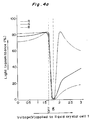
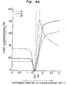
- Figs. 4a and 4b are graphs of characteristic curves showing the relation between a voltage applied to the liquid crystal layer 6a of the first cell layer 1 and a light transmittance in the double-layered-type liquid crystal device shown in Fig. 1, wherein Fig. 4a shows the characteristics in the case of a monochromatic display, and Fig. 4b shows the characteristics in the case of a multicolor display.
- an ON voltage of about 1.7 V or an OFF voltage of about 1.5 V is selectively applied between the transparent electrode films 4a and 4b of the first cell layer 1 with use of a simple multiplex driving method so as to be applied to the liquid crystal layer 6a.
- the orientation direction of the liquid crystal molecules on each pixel of an area of the liquid crystal layer 6a where the transparent electrode films 4a and 4b cross each other changes according to the voltage applied thereto.
- the light having passed through the first and second cell layers 1 and 2 passes through the polarizer 8b when the OFF voltage is applied to the liquid crystal layer 6a.
- the light having passed through the first and second layers 1 and 2 is shaded by the polarizer 8b when the ON voltage is applied thereto.
- red color light R having a wavelength of 610 nm, green color light G having a wavelength of 550 nm and blue color light B having a wavelength of 450 nm are incident substantially perpendicularly to the outer surface of the polarizer 8a from the outer side thereof to the liquid crystal device, they pass through each partial area of the polarizer 8b corresponding to each of a first group of pixels of the liquid crystal layer 6a to which the OFF voltage is applied, and then, a white color image is displayed on each of the first group of pixels.
- the red color light R, the green color light G and the blue color light B are shaded by each partial area of the polarizer 8b corresponding to each of a second group of pixels of the liquid crystal layer 6a to which the ON voltage is applied, and then, a black color image is displayed on each of the second group of pixels. Therefore, a monochromatic image composed of white and black color images is displayed on the double-layered-type liquid crystal device.
- the second cell layer 2 acts as a compensator for compensating a color tone of the light having passed through the first cell layer 1, resulting in an excellent monochromatic display without interference colors.
- the ON or OFF voltage is selectively applied to the liquid crystal layer 6a of the first cell layer 1 in the manner similar to the case of the aforementioned monochromatic display. Then, as shown in Fig. 4b, the red color light R, the green color light G and the blue color light B are shaded by each partial area of the polarizer 8b corresponding to each of a first group of pixels of the liquid crystal layer 6a to which the OFF voltage is applied, and then, a black color image is displayed on each of the first group of pixels.
- the light transmittance of only the blue color light B on each of a second group of pixels corresponding to the liquid crystal layer 6a to which the ON voltage is applied increases, and then, a blue color image is displayed on each of the second group of pixels. Therefore, a two-color image composed of black and blue color images is displayed on the double-layered-type liquid crystal device.
- the characteristic of the function for compensating the color tone of the second cell layer 2 changes by switching over from such a state that the predetermined voltage is applied to the liquid crystal layer 6b to such a state that no voltage is applied thereto, resulting in a change in the color of the displayed image.
- the whole image surface of the double-layered-type liquid crystal device can be switched over from a monochromatic display for selectively displaying a white color image or a black color image thereon to a two-color display for selectively displaying a black color image or a blue color image thereon.
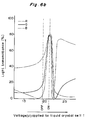
- Fig. 5a and 5b are graphs of characteristic curves showing the relation between a voltage applied to a liquid crystal layer 6a of a first cell layer 1 and a light transmittance in a double-layered-type liquid crystal device of a second preferred embodiment according to the present invention, wherein Fig. 5a shows the characteristics in the case of a monochromatic display, and Fig. 5b shows the characteristics in the case of a multicolor display.
- the double-layered-type liquid crystal device of the second preferred embodiment has a structure similar to that of the first preferred embodiment. Therefore, the composition of the double-layered-type liquid crystal device of the second preferred embodiment will be described below with reference to Fig. 1.
- transparent substrates 3a to 3c are made of glass. After films of ITO having a thickness of about 1500 ⁇ are deposited on the inner surface of the transparent substrate 3a, both the surfaces of the transparent substrate 3b and the inner surface of the transparent substrate 3c by the vapor deposition method, they are etched so as to have desirable patterns, resulting in transparent electrical conductive electrode films 4a to 4d formed thereon. On each of the transparent electrode films 4a to 4d, orientation membranes 5aa, 5ab, 5ba and 5bb of polyimide are formed with a thickness of about 500 ⁇ by a spin coating technique, the surfaces of which are treated by rubbing with cloth, causing the liquid crystal molecules to be in a parallel orientation.
- a liquid crystal layer 6a of the first cell layer 1 is made of a liquid crystal ZLI-1691 made by Merck & Co., Inc., to which 0.72 wt% of cholesteryl nonanoate is added as an optically active material.
- a liquid crystal layer 6b of the second cell layer 2 is made of a liquid crystal ZLI-3449-000 made by Merck & Co., Inc., to which 1.0 wt% of CB-15 is added.
- the twist direction of the liquid crystal layer 6a is opposite to that of the liquid crystal layer 6b, and the twist angles ⁇ 1 and ⁇ 2 of the liquid crystal layers 6a and 6b are set at 240° and 270°, respectively.
- the thickness d1 of the first cell layer 1 is about 7 ⁇ m
- the thickness d2 of the second cell layer 2 is about 12 ⁇ m
- the pitch p of the helical twist of the liquid crystal layer 6a is about 14 ⁇ m
- that of the liquid crystal layer 6b is about 20 ⁇ m.
- the pretilt angle of each of the liquid crystal arranged between the orientation membranes 5aa and 5ab and the liquid crystal arranged between the orientation membranes 5ba and 5bb are set at about 8°.
- the polarizers 8a and 8b are made of a compound including iodine, and are formed on the outer surfaces of the outer transparent substrates 3a and 3c so that the polarization axes thereof cross each other at an angle of 30°.
- the ON or OFF voltage is selectively applied to the liquid crystal layer 6a of the first cell layer 1 under the condition that the predetermined voltage is applied to the liquid crystal layer 6b of the second cell layer 2 so as to display a monochromatic image on the double-layered-type liquid crystal device.
- the ON or OFF voltage is selectively applied to the liquid crystal layer 6a of the first cell layer 1 under the condition that no voltage is applied to the liquid crystal layer 6b of the second cell layer 2 so as to display a two-color image thereon based on interference colors.
- an ON voltage of about 2.2 V or an OFF voltage of about 2.0 V is selectively applied between the transparent electrode films 4a and 4b of the first cell layer 1. Then, the light having passed through the first and second cell layers 1 and 2 passes through the polarizer 8b when the OFF voltage is applied to the liquid crystal layer 6a. On the other hand, the light having passed therethrough is shaded by the polarizer 8b when the ON voltage is applied thereto.
- the red color light R, the green color light G and the blue color light B pass through each partial area of the polarizer 8b corresponding to each of a first group of pixels of the liquid crystal layer 6a to which the OFF voltage is applied, and then, a white color image is displayed on each of the first group of pixels.
- the red color light R, the green color light G and the blue color light B are shaded by each partial area of the polarizer 8b corresponding to each of a second group of pixels of the liquid crystal layer 6a to which the ON voltage is applied, and then, a black color image is displayed on each of the second group of pixels. Therefore, a monochromatic image composed of white and black color images is displayed on the double-layered-type liquid crystal device.
- the second cell layer 2 acts as a compensator, resulting in an excellent monochromatic display without interference colors in the manner similar to that of the first preferred embodiment.
- the ON or OFF voltage is selectively applied to the liquid crystal layer 6a of the first cell layer 1 in the manner similar to the case of the aforementioned monochromatic display. Then, as shown in Fig. 5b, the light transmittance of only the blue color light B on each of a first group of pixels of the liquid crystal layer 6a to which the OFF voltage is applied increases. On the other hand, the light transmittance of only the green color light G on each of a second group of pixels of the liquid crystal layer 6a to which the ON voltage is applied increases. Therefore, a two-color image composed of blue and green color images is displayed on the double-layered-type liquid crystal device.
- the whole image surface of the double-layered-type liquid crystal device can be switched over from a monochromatic display for selectively displaying a white color image or a black color image thereon to a two-color display for selectively displaying a green color image or a blue color image thereon.
- Figs. 6a and 6b are graphs of characteristic curves showing the relation between a voltage applied to a liquid crystal layer 6a of a first cell layer 1 and a light transmittance in a double-layered-type liquid crystal device of a third preferred embodiment according to the present invention, wherein Fig. 6a shows the characteristics in the case of a monochromatic display, and Fig. 6b shows the characteristics in the case of a multicolor display.
- the double-layered-type liquid crystal device of the third preferred embodiment has a structure similar to that of the first preferred embodiment. Therefore, the composition of the double-layered-type liquid crystal device of the third preferred embodiment will be described below with reference to Fig. 1.
- the liquid crystal layers 6a and 6b of the first and second cell layers 1 and 2 are made of a liquid crystal ZLI-1691 made by Merck & Co., Inc., wherein 0.63 wt% of cholesteryl nonanoate is added as an optically active material to the liquid crystal layer 6a, and 0.93 wt% of CB-15 is added as the optically active material to the liquid crystal layer 6b.
- the twist direction of the liquid crystal layer 6a is opposite to that of the liquid crystal layer 6b, and each of the twist angles ⁇ 1 and ⁇ 2 of the liquid crystal layers 6a and 6b is set at 240°.
- the thickness d1 of the first cell layer 1 is about 8 ⁇ m
- the thickness d2 of the second cell layer 2 is about 7.5 ⁇ m.
- the pitch p of the helical twist of the liquid crystal layer 6a is about 16 ⁇ m
- that of the liquid crystal layer 6b is about 15 ⁇ m.
- the polarizers 8a and 8b are formed on the outer surfaces of the outer transparent substrates 3a and 3c so that the polarization axes thereof cross each other at an angle of zero, namely, the polarization axes thereof become parallel.
- the other values are set at the same values as that of the second preferred embodiment.
- the ON or OFF voltage is selectively applied to the liquid crystal layer 6a of the first cell layer 1 under the condition that no voltage is applied to the liquid crystal layer 6b of the second cell layer 2 so as to display a monochromatic image on the double-layered-type liquid crystal device.
- the ON or OFF voltage is selectively applied to the liquid crystal layer 6a of the first cell layer 1 under the condition that a predetermined voltage is applied to the liquid crystal layer 6b of the second cell layer 2 so as to display a multicolor image thereon based on interference colors.
- an ON voltage of about 2,2 V or an OFF voltage of about 2.0 V is selectively applied between the transparent electrode films 4a and 4b of the first cell layer 1. Then, the light passes through the polarizer 8b when the OFF voltage is applied to the liquid crystal layer 6a. On the other hand, the light is shaded by the polarizer 8b when the ON voltage is applied thereto.
- the red color light R, the green color light G and the blue color light B pass through each partial area of the polarizer 8b corresponding to each of a first group of pixels of the liquid crystal layer 6a to which the OFF voltage is applied, and then, a white color image is displayed on each of the first group of pixels.
- the red color light R, the green color light G and the blue color light B are shaded by each partial area of the polarizer 8b corresponding to each of a second group of pixels of the liquid crystal layer 6a to which the ON voltage is applied, and then, a black color image is displayed on each of the second group of pixels. Therefore, a monochromatic image composed of white and black color images is displayed on the double-layered-type liquid crystal device.
- the second cell layer 2 acts as a compensator, resulting in an excellent monochromatic display without interference colors in the manner similar to that of the first preferred embodiment.
- the ON or OFF voltage is selectively applied to the liquid crystal layer 6a of the first cell layer 1 in the manner similar to the case of the aforementioned monochromatic display. Then, as shown in Fig. 6b, respective light transmittances of both the red color light R and the green color light G on each of a first group of pixels of the the liquid crystal layer 6a to which the OFF voltage is applied decrease, and then, a yellow color image is displayed on each of the first group of pixels.
- the red color light R, the green color light G and the blue color light B pass through each partial area of the polarizer 8b corresponding to each of a second group of pixels of the liquid crystal layer 6a to which the ON voltage is applied, and then, a white color image is displayed on each of the second group of pixels. Therefore, a two-color image composed of yellow and white color images is displayed on the double-layered-type liquid crystal device.
- the whole image surface of the double-layered-type liquid crystal device can be switched over from a monochromatic display for selectively displaying a white color image or a black color image thereon to a two-color display for selectively displaying a yellow color image or a white color image thereon.
- the double-layered-type liquid crystal device is described above; however the present invention is not limited to this construction.
- the present invention can be applied to a multi-layered-type liquid crystal device.
Landscapes
- Physics & Mathematics (AREA)
- Nonlinear Science (AREA)
- Mathematical Physics (AREA)
- Chemical & Material Sciences (AREA)
- Crystallography & Structural Chemistry (AREA)
- General Physics & Mathematics (AREA)
- Optics & Photonics (AREA)
- Liquid Crystal (AREA)
- Liquid Crystal Display Device Control (AREA)
- Devices For Indicating Variable Information By Combining Individual Elements (AREA)
Claims (13)
- Verfahren zum Ansteuern einer mehrschichtigen Flüssigkristall-Anzeigevorrichtung mit mehreren aufeinandergeschichteten Zellenschichten (1, 2), von denen jede ein Flüssigkristallmaterial (6a, 6b) mit zwischen zwei transparenten Substraten (3a, 3b; 3b, 3c) verdrillten Molekülen enthält, um große Doppelbrechung aufzuweisen, wobei die Vorrichtung ferner zwei die mehreren aufeinandergeschichteten Zellenschichten einbettenden Polarisatoren (8a, 8b) aufweist, wobei gemäß dem Verfahren eine Ansteuerspannung an mindestens eine (1) der Zellenschichten angelegt wird, gekennzeichnet durch ein Einstellen einer Spannung an einer weiteren (2) der Zellenschichten, um die Farbe des durch die Vorrichtung angezeigten Bilds ausschließlich durch die Wechselwirkung zwischen der Polarisationsfilterung durch die Polarisatoren und den Interferenzeffekten zu bestimmen, wie sie durch die Doppelbrechung des Flüssigkristallmaterials (6a, 6b) der einzelnen Zellenschichten unter dem Einfluß der Spannungen hervorgerufen werden.
- Verfahren nach Anspruch 1, bei dem die an mindestens eine Zellenschicht (2) angelegte Spannung festgehalten wird und die an die anderen Zellenschichten (1) angelegten Spannungen zwischen verschiedenen vorgegebenen Spannungen umgeschaltet werden.
- Verfahren nach einem der Ansprüche 1 oder 2, bei dem die Flüssigkristall-Anzeigevorrichtung eine zweischichtige Flüssigkristall-Anzeigevorrichtung ist, die aus einer ersten und einer zweiten Zellenschicht (1, 2) besteht.
- Verfahren nach Anspruch 3, bei dem die Beziehung zwischen dem Produkt aus der Doppelbrechung Δn₁, der Dicke d₁ und dem Verdrillungswinkel Θ₁ für die erste Zellenschicht (1) und dem Produkt aus der Doppelbrechung Δn₂, der Dicke d₂ und dem Verdrillungswinkel Θ₂ für die zweite Zellenschicht (2) so eingestellt ist, daß sie der folgenden Ungleichung genügt:
 - Anlegen einer vorgegebenen Spannung an die zweite Zellenschicht (2) und- selektives Anlegen einer ersten vorgegebenen Spannung oder einer zweiten vorgegebenen Spannung an die erste Zellenschicht (1), um dadurch ein monochromes Bild auf der Flüssigkristall-Anzeigevorrichtung anzuzeigen.
 - Verfahren nach Anspruch 3, bei dem die Beziehung zwischen dem Produkt aus der Doppelbrechung Δn₁, der Dicke d₁ und dem Verdrillungswinkel Θ₁ für die erste Zellenschicht (1) und dem Produkt aus der Doppelbrechung Δn₂, der Dicke d₂ und dem Verdrillungswinkel Θ₂ für die zweite Zellenschicht (2) so eingestellt ist, daß sie der folgenden Ungleichung genügt:
 - Anlegen keiner Spannung an die zweite Zellenschicht (2) und- selektives Anlegen einer ersten vorgegebenen Spannung oder einer zweiten vorgegebenen Spannung an die erste Zellenschicht (1), um dadurch ein zweifarbiges Bild auf der Flüssigkristall-Anzeigevorrichtung anzuzeigen.
 - Verfahren nach Anspruch 3, bei dem die Beziehung zwischen dem Produkt aus der Doppelbrechung Δn₁, der Dicke d₁ und dem Verdrillungswinkel Θ₁ für die erste Zellenschicht (1) und dem Produkt aus der Doppelbrechung Δn₂, der Dicke d₂ und dem Verdrillungswinkel Θ₂ für die zweite Zellenschicht (2) so eingestellt ist, daß sie der folgenden Ungleichung genügt:
 - Anlegen keiner Spannung an die zweite Zellenschicht (2) und- selektives Anlegen einer ersten vorgegebenen Spannung oder einer zweiten vorgegebenen Spannung an die erste Zellenschicht (1), um dadurch ein monochromes Bild auf der Flüssigkristall-Anzeigevorrichtung anzuzeigen.
 - Verfahren nach Anspruch 3, bei dem die Beziehung zwischen dem Produkt aus der Doppelbrechung Δn₁, der Dicke d₁ und dem Verdrillungswinkel Θ₁ für die erste Zellenschicht (1) und dem Produkt aus der Doppelbrechung Δn₂, der Dicke d₂ und dem Verdrillungswinkel Θ₂ für die zweite Zellenschicht (2) so eingestellt ist, daß sie der folgenden Ungleichung genügt:
 - Anlegen einer vorgegebenen Spannung an die zweite Zellenschicht (2) und- selektives Anlegen einer ersten vorgegebenen Spannung oder einer zweiten vorgegebenen Spannung an die erste Zellenschicht, zum Anzeigen eines zweifarbigen Bilds auf der Flüssigkristall-Anzeigevorrichtung.
 - Verfahren nach einem der Ansprüche 3 bis 7, bei dem- der Absolutwert des Produkts aus der Doppelbrechung Δn₁ und der Dicke d₁ der ersten Zellenschicht (1) so eingestellt ist, daß die folgende Ungleichung erfüllt ist:
 - der Absolutwert des Produkts aus der Doppelbrechung Δn₂ und der Dicke d₂ der zweiten Zellenschicht (2) so eingestellt ist, daß die folgende Ungleichung erfüllt ist:
- Verfahren nach einem der Ansprüche 3, 4 oder 6, bei dem das Verhältnis aus dem Produkt der Doppelbrechung Δn₂ und der Dicke d₂ der zweiten Zellenschicht (2) zum Produkt aus der Doppelbrechung Δn₁ und der Dicke d₁ der ersten Zellenschicht (1) so eingestellt ist, daß die folgende Ungleichung erfüllt ist:

- Verfahren nach einem der Ansprüche 3, 4 oder 6, bei dem- der Verdrillungswinkel der ersten Zellenschicht (1) so eingestellt wird, daß er in den Bereich von 180° bis 360° fällt; und- der Verdrillungswinkel der zweiten Zellenschicht (2) so eingestellt ist, daß er in den Bereich von 30° bis 360° fällt und sich von dem der ersten Zellenschicht (1) unterscheidet.
- Verfahren nach einem der Ansprüche 3 bis 7, bei dem das Verhältnis aus der Dicke d der ersten (1) und der zweiten (2) Zellenschicht zur Schraubenganghöhe p des darin enthaltenen Flüssigkristalls so eingestellt ist, daß die folgende Ungleichung erfüllt ist, wenn der Vorneigungswinkel des dort vorhandenen Flüssigkristalls 10° entspricht oder kleiner ist:

- Verfahren nach einem der Ansprüche 4 bis 11, ferner mit dem Schritt des Umschaltens zwischen- einem Zustand, in dem eine vorgegebene Spannung an die zweite Zellenschicht (2) angelegt wird und eine erste vorgegebene Spannung oder eine zweite vorgegebene Spannung selektiv an die erste Zellenschicht (1) angelegt wird; und- einem Zustand, in dem die Spannung null an die zweite Zellenschicht (2) angelegt wird und eine erste vorgegebene Spannung oder eine zweite vorgegebene Spannung selektiv an die erste Zellenschicht (1) angelegt wird.
- Flüssigkristall-Anzeigevorrichtung mit:- mehreren aufeinandergeschichteten Flüssigkristallzelle-Schichten (1, 2), von denen jede ein Flüssigkristallmaterial (6a, 6b) enthält, das zwischen zwei transparenten Substraten (3a, 3b; 3b, 3c) verdrillt ist, um große Doppelbrechung zu aufzuweisen, die abhängig von der an die jeweilige Zellenschicht angelegten Spannung variiert, wobei die Vorrichtung ferner folgendes aufweist:- zwei Polarisatoren (8a, 8b), die so angeordnet sind, daß sie die mehreren aufeinandergeschichteten Flüssigkristallschichten einbetten; und- eine erste Elektrodeneinrichtung (4a, 4b) zum Anlegen einer Ansteuerspannung an eine erste (1) der Zellenschichten; gekennzeichnet durch- eine zweite Elektrodeneinrichtung (4c, 4d) zum Einstellen einer an eine zweite (2) der Zellenschichten angelegten Spannung;- wobei die Farbe des durch die Vorrichtung angezeigten Bilds ausschließlich durch die Wechselwirkung zwischen der Polarisationsfilterung durch die Polarisatoren und den Interferenzeffekten bestimmt wird, wie sie durch die Doppelbrechung des Flüssigkristallmaterials (6a, 6b) der einzelnen Zellenschichten unter dem Einfluß der Spannungen hervorgerufen werden.
Applications Claiming Priority (2)
| Application Number | Priority Date | Filing Date | Title |
|---|---|---|---|
| JP63294373A JP2598495B2 (ja) | 1988-11-21 | 1988-11-21 | 液晶表示装置の駆動方法 |
| JP294373/88 | 1988-11-21 |
Publications (3)
| Publication Number | Publication Date |
|---|---|
| EP0370773A2 EP0370773A2 (de) | 1990-05-30 |
| EP0370773A3 EP0370773A3 (en) | 1990-11-07 |
| EP0370773B1 true EP0370773B1 (de) | 1996-01-17 |
Family
ID=17806877
Family Applications (1)
| Application Number | Title | Priority Date | Filing Date |
|---|---|---|---|
| EP89312086A Expired - Lifetime EP0370773B1 (de) | 1988-11-21 | 1989-11-21 | Ansteuerungsverfahren einer mehrschichtigen Flüssigkristall-Anzeigevorrichtung |
Country Status (4)
| Country | Link |
|---|---|
| US (1) | US5090794A (de) |
| EP (1) | EP0370773B1 (de) |
| JP (1) | JP2598495B2 (de) |
| DE (1) | DE68925468T2 (de) |
Families Citing this family (24)
| Publication number | Priority date | Publication date | Assignee | Title |
|---|---|---|---|---|
| KR960004147B1 (ko) * | 1989-11-20 | 1996-03-27 | 쓰지 하루오 | 컬러액정표시장치 |
| JPH0498223A (ja) * | 1990-08-17 | 1992-03-30 | Nec Corp | 液晶素子 |
| JP2721284B2 (ja) * | 1991-02-07 | 1998-03-04 | 株式会社東芝 | 液晶表示素子および光学異方素子 |
| JP2680484B2 (ja) * | 1991-05-20 | 1997-11-19 | シャープ株式会社 | 光書き込み型液晶表示装置 |
| US5457551A (en) * | 1993-10-08 | 1995-10-10 | Planar Systems, Inc. | Frame response compensated, video rate addressable liquid crystal passive matrix display system |
| US6985127B1 (en) | 1994-09-01 | 2006-01-10 | The United States Of America As Represented By The Secretary Of The Navy | Programmable gray-scale liquid crystal display |
| GB2299698A (en) * | 1995-03-30 | 1996-10-09 | Sharp Kk | Colour display |
| EP0774131A1 (de) * | 1995-06-07 | 1997-05-21 | Asahi Glass Company Ltd. | Reflektive farbflüssigkristallanzeige |
| GB2314641A (en) * | 1996-06-26 | 1998-01-07 | Sharp Kk | Liquid crystal devices |
| GB2314640A (en) * | 1996-06-26 | 1998-01-07 | Sharp Kk | Liquid crystal devices |
| US6812624B1 (en) * | 1999-07-20 | 2004-11-02 | Sri International | Electroactive polymers |
| JP3547712B2 (ja) * | 2001-02-13 | 2004-07-28 | ナノックス株式会社 | 反射型液晶表示装置とその製造方法 |
| TWI233500B (en) * | 2001-04-23 | 2005-06-01 | Reveo Inc | Image display system and electrically actuatable image combiner therefor |
| JP4033148B2 (ja) * | 2004-03-03 | 2008-01-16 | ソニー株式会社 | レンズ鏡筒および撮像装置 |
| WO2009006318A1 (en) | 2007-06-29 | 2009-01-08 | Artificial Muscle, Inc. | Electroactive polymer transducers for sensory feedback applications |
| EP2239793A1 (de) | 2009-04-11 | 2010-10-13 | Bayer MaterialScience AG | Elektrisch schaltbarer Polymerfilmaufbau und dessen Verwendung |
| US9464769B2 (en) * | 2009-09-11 | 2016-10-11 | Dolby Laboratories Licensing Corporation | Techniques for using quantum dots to regenerate light in display systems |
| WO2012118916A2 (en) | 2011-03-01 | 2012-09-07 | Bayer Materialscience Ag | Automated manufacturing processes for producing deformable polymer devices and films |
| TW201250288A (en) | 2011-03-22 | 2012-12-16 | Bayer Materialscience Ag | Electroactive polymer actuator lenticular system |
| WO2013142552A1 (en) | 2012-03-21 | 2013-09-26 | Bayer Materialscience Ag | Roll-to-roll manufacturing processes for producing self-healing electroactive polymer devices |
| KR20150031285A (ko) | 2012-06-18 | 2015-03-23 | 바이엘 인텔렉쳐 프로퍼티 게엠베하 | 연신 공정을 위한 연신 프레임 |
| US9590193B2 (en) | 2012-10-24 | 2017-03-07 | Parker-Hannifin Corporation | Polymer diode |
| WO2015148244A2 (en) | 2014-03-26 | 2015-10-01 | Dolby Laboratories Licensing Corporation | Global light compensation in a variety of displays |
| US11151914B1 (en) * | 2020-04-09 | 2021-10-19 | Nvidia Corporation | Defective pixel identification and mitigation in multi-layer liquid crystal displays |
Family Cites Families (16)
| Publication number | Priority date | Publication date | Assignee | Title |
|---|---|---|---|---|
| JPS5927915B2 (ja) * | 1976-07-09 | 1984-07-09 | 松下電器産業株式会社 | 液晶表示装置 |
| JPS53101296A (en) * | 1977-02-16 | 1978-09-04 | Seiko Epson Corp | Display unit |
| JPS5536802A (en) * | 1978-07-25 | 1980-03-14 | Asahi Glass Co Ltd | Liquid crystal color display device |
| JPS55166619A (en) * | 1979-06-15 | 1980-12-25 | Stanley Electric Co Ltd | Multilayer liquid crystal display device |
| JPS5667817A (en) * | 1979-11-09 | 1981-06-08 | Canon Inc | Liquid crystal indicator |
| JPS5792311A (en) * | 1980-11-28 | 1982-06-08 | Sharp Corp | Guest-host type liquid crystal display element |
| US4443065A (en) * | 1980-12-09 | 1984-04-17 | Sharp Kabushiki Kaisha | Interference color compensation double layered twisted nematic display |
| JPS6019123A (ja) * | 1983-07-13 | 1985-01-31 | Stanley Electric Co Ltd | 液晶表示装置 |
| JPH0656459B2 (ja) * | 1985-04-05 | 1994-07-27 | 株式会社日立製作所 | 液晶表示素子 |
| EP0246842B1 (de) * | 1986-05-19 | 1998-09-23 | Seiko Epson Corporation | Flüssigkristall-Anzeigevorrichtung |
| JPS62283684A (ja) * | 1986-06-02 | 1987-12-09 | Hitachi Ltd | 光プロ−ブ装置 |
| JPS63234225A (ja) * | 1987-03-23 | 1988-09-29 | Sharp Corp | 液晶表示装置 |
| JPS6444417A (en) * | 1987-08-12 | 1989-02-16 | Matsushita Electric Industrial Co Ltd | Liquid crystal display device |
| JP2560449B2 (ja) * | 1987-10-06 | 1996-12-04 | 旭硝子株式会社 | 液晶表示素子及びその製造方法 |
| JPH0797189B2 (ja) * | 1987-10-07 | 1995-10-18 | シャープ株式会社 | 液晶表示装置 |
| EP0312297B1 (de) * | 1987-10-13 | 1994-01-26 | Fujitsu Limited | Flüssigkristall-Anzeigetafel |
-
1988
- 1988-11-21 JP JP63294373A patent/JP2598495B2/ja not_active Expired - Lifetime
-
1989
- 1989-11-21 US US07/439,876 patent/US5090794A/en not_active Expired - Lifetime
- 1989-11-21 EP EP89312086A patent/EP0370773B1/de not_active Expired - Lifetime
- 1989-11-21 DE DE68925468T patent/DE68925468T2/de not_active Expired - Fee Related
Also Published As
| Publication number | Publication date |
|---|---|
| DE68925468T2 (de) | 1996-07-04 |
| US5090794A (en) | 1992-02-25 |
| EP0370773A3 (en) | 1990-11-07 |
| JPH02140720A (ja) | 1990-05-30 |
| EP0370773A2 (de) | 1990-05-30 |
| JP2598495B2 (ja) | 1997-04-09 |
| DE68925468D1 (de) | 1996-02-29 |
Similar Documents
| Publication | Publication Date | Title |
|---|---|---|
| US5090794A (en) | Method for driving a multi-layered-type liquid crystal display device | |
| EP0284372B1 (de) | Flüssigkristall-Anzeigevorrichtung | |
| EP0311405B1 (de) | Flüssigkristall-Anzeigevorrichtung | |
| EP0351200B1 (de) | Flüssigkristall-Anzeigevorrichtung | |
| EP0319351B1 (de) | Flüssigkristall-Anzeigevorrichtung | |
| EP0333881B1 (de) | Flüssigkristall-anzeigevorrichtung | |
| EP0352101B1 (de) | Doppelschicht-Flüssigkristall-Anzeigevorrichtung | |
| JP2768319B2 (ja) | カラー液晶表示素子 | |
| JP2768977B2 (ja) | 液晶素子及びそれを用いた装置 | |
| JPH01254917A (ja) | 液晶表示素子及びそれを使用したoa機器 | |
| JP2775823B2 (ja) | 液晶表示素子 | |
| JP2775827B2 (ja) | 液晶表示素子 | |
| EP0390544A2 (de) | Doppelschicht-Flüssigkristall-Anzeigevorrichtung | |
| JP2625851B2 (ja) | 液晶表示素子及びそれを使用した液晶表示装置 | |
| JP2819602B2 (ja) | 液晶表示素子 | |
| JPH02821A (ja) | 液晶表示素子 | |
| JP3843157B2 (ja) | 液晶表示装置 | |
| JPH04179922A (ja) | 液晶表示素子 | |
| JPH0247625A (ja) | 液晶表示素子 | |
| JPH02167526A (ja) | 液晶装置 | |
| JPH01137233A (ja) | 液晶表示素子 | |
| JPH09325315A (ja) | 液晶装置 | |
| JPH11316363A (ja) | 液晶装置 | |
| JPH02275412A (ja) | 液晶表示素子 | |
| JPH0588155A (ja) | カラー液晶表示装置 |
Legal Events
| Date | Code | Title | Description |
|---|---|---|---|
| PUAI | Public reference made under article 153(3) epc to a published international application that has entered the european phase |
Free format text: ORIGINAL CODE: 0009012 |
|
| AK | Designated contracting states |
Kind code of ref document: A2 Designated state(s): DE FR GB |
|
| PUAL | Search report despatched |
Free format text: ORIGINAL CODE: 0009013 |
|
| AK | Designated contracting states |
Kind code of ref document: A3 Designated state(s): DE FR GB |
|
| 17P | Request for examination filed |
Effective date: 19901128 |
|
| 17Q | First examination report despatched |
Effective date: 19930422 |
|
| GRAA | (expected) grant |
Free format text: ORIGINAL CODE: 0009210 |
|
| AK | Designated contracting states |
Kind code of ref document: B1 Designated state(s): DE FR GB |
|
| REF | Corresponds to: |
Ref document number: 68925468 Country of ref document: DE Date of ref document: 19960229 |
|
| ET | Fr: translation filed | ||
| PLBE | No opposition filed within time limit |
Free format text: ORIGINAL CODE: 0009261 |
|
| STAA | Information on the status of an ep patent application or granted ep patent |
Free format text: STATUS: NO OPPOSITION FILED WITHIN TIME LIMIT |
|
| 26N | No opposition filed | ||
| PGFP | Annual fee paid to national office [announced via postgrant information from national office to epo] |
Ref country code: FR Payment date: 20011113 Year of fee payment: 13 |
|
| PGFP | Annual fee paid to national office [announced via postgrant information from national office to epo] |
Ref country code: GB Payment date: 20011121 Year of fee payment: 13 |
|
| PGFP | Annual fee paid to national office [announced via postgrant information from national office to epo] |
Ref country code: DE Payment date: 20011203 Year of fee payment: 13 |
|
| REG | Reference to a national code |
Ref country code: GB Ref legal event code: IF02 |
|
| PG25 | Lapsed in a contracting state [announced via postgrant information from national office to epo] |
Ref country code: GB Free format text: LAPSE BECAUSE OF NON-PAYMENT OF DUE FEES Effective date: 20021121 |
|
| PG25 | Lapsed in a contracting state [announced via postgrant information from national office to epo] |
Ref country code: DE Free format text: LAPSE BECAUSE OF NON-PAYMENT OF DUE FEES Effective date: 20030603 |
|
| GBPC | Gb: european patent ceased through non-payment of renewal fee | ||
| PG25 | Lapsed in a contracting state [announced via postgrant information from national office to epo] |
Ref country code: FR Free format text: LAPSE BECAUSE OF NON-PAYMENT OF DUE FEES Effective date: 20030731 |
|
| REG | Reference to a national code |
Ref country code: FR Ref legal event code: ST |