EP0371792A2 - Comparaison de caractéristiques - Google Patents
Comparaison de caractéristiques Download PDFInfo
- Publication number
- EP0371792A2 EP0371792A2 EP89312454A EP89312454A EP0371792A2 EP 0371792 A2 EP0371792 A2 EP 0371792A2 EP 89312454 A EP89312454 A EP 89312454A EP 89312454 A EP89312454 A EP 89312454A EP 0371792 A2 EP0371792 A2 EP 0371792A2
- Authority
- EP
- European Patent Office
- Prior art keywords
- feature
- signal
- scan
- pulse
- line
- Prior art date
- Legal status (The legal status is an assumption and is not a legal conclusion. Google has not performed a legal analysis and makes no representation as to the accuracy of the status listed.)
- Withdrawn
Links
Images


Classifications
-
- G—PHYSICS
- G01—MEASURING; TESTING
- G01B—MEASURING LENGTH, THICKNESS OR SIMILAR LINEAR DIMENSIONS; MEASURING ANGLES; MEASURING AREAS; MEASURING IRREGULARITIES OF SURFACES OR CONTOURS
- G01B7/00—Measuring arrangements characterised by the use of electric or magnetic techniques
- G01B7/004—Measuring arrangements characterised by the use of electric or magnetic techniques for measuring coordinates of points
-
- G—PHYSICS
- G06—COMPUTING OR CALCULATING; COUNTING
- G06V—IMAGE OR VIDEO RECOGNITION OR UNDERSTANDING
- G06V10/00—Arrangements for image or video recognition or understanding
- G06V10/40—Extraction of image or video features
- G06V10/44—Local feature extraction by analysis of parts of the pattern, e.g. by detecting edges, contours, loops, corners, strokes or intersections; Connectivity analysis, e.g. of connected components
- G06V10/457—Local feature extraction by analysis of parts of the pattern, e.g. by detecting edges, contours, loops, corners, strokes or intersections; Connectivity analysis, e.g. of connected components by analysing connectivity, e.g. edge linking, connected component analysis or slices
-
- G—PHYSICS
- G06—COMPUTING OR CALCULATING; COUNTING
- G06V—IMAGE OR VIDEO RECOGNITION OR UNDERSTANDING
- G06V10/00—Arrangements for image or video recognition or understanding
- G06V10/40—Extraction of image or video features
- G06V10/42—Global feature extraction by analysis of the whole pattern, e.g. using frequency domain transformations or autocorrelation
Definitions
- the invention provides a method and apparatus for determining the location, and preferably also the area, of a particular feature within a field of view. In one application of the invention it may be required to determine, for example, whether a component such as a memory chip is correctly located on a printed circuit board.
- the field of view is scanned to obtain a video signal representing the feature, and this signal is processed to obtain the co- ordinates of a unique point representing the position of the feature, and preferably also to obtain a measure of the feature area.
- the position and area so determined may be compared with those for an ideal case, for example if the object being scanned is a printed circuit board, the data may be compared with similar data obtained by scanning a board which has been checked and is known to be accurate, or with data for an ideal board which have been determined and stored in memory.
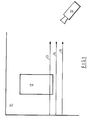
- a video camera 10 is arranged to scan a field of view 11 containing a feature 12 of rectangular outline.
- the field of view may be occupied by a printed circuit board, and the feature may be an integrated circuit chip mounted on the board, and whose position is to be checked.
- the last scan intersecting the feature and the next two succeeding scans are shown at 13, 14 and 15 respectively, with their spacings very much exaggerated for purposes of explanation.
- the grey scale of the video system is adjusted and the video signal is processed so that the output signal is a binary signal having the value "0" for the background and the value "1" where the scan crosses the feature.
- One circuit suitable for this purpose is described in our pending Irish patent application serial no 1234/88. Referring for a moment to Figure 3, the output signal for the scan 13 of
- Figure 1 is represented by waveform E.
- the video signals so obtained are processed so as to obtain, for each feature, the co-ordinates of a uniquely defined point characterising the position of the feature, and preferably also a measure of the area of each feature.
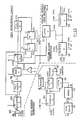
- the circuit of Figure 2 generates a feature position pulse at such a characteristic point.
- the scan signal E is delayed in a delay line 201 by a time equal to one scan interval to give a delayed signal F, and both the original signal E and the delayed signal F are combined by an OR gate 202 and applied to a latch 203, which is set by the leading edge of the signal.
- the output of the latch 203 is delayed by two pixels less than one scan line by the delay line 204 to give a signal K and this is combined in an OR gate 205 to provide a signal whose trailing edge resets the latch 203.
- the signal K is further delayed by two pixels by the delay line 206 to give a signal R, which corresponds exactly with the scan signal E, but is delayed by one scan line, or, in the case of the final scan of a feature, when the latch 203 is set by the delayed signal F, by two scan lines.
- This signal is applied to a monostable or trigger 207 which responds to its trailing edge to generate a pulse H of 0.5 pixel in length.
- a gating signal is generated from the output of the latch 203 by delaying the signal by three pixels by means of a delay 208 and ORing the latch output with the delayed signal in an OR gate 209 to give a signal T which is stretched by three pixels. This is inverted by an inverting amplifier 210 and applied as one input of an AND gate 211, the other input of which receives the signal pulse H. The output of this AND gate provides the feature position pulse J, as will be explained below.
- the pulse H is also applied to a trigger or monostable 212 which responds to its trailing edge by generating a further pulse signal L.
- the signal L must occur later than the trailing edge of the feature on each scan by at least the width of the pulse H, and this signal is made use of in the area measuring circuits to be described below. The operation of this circuit will now be described with reference to the scan lines of Figure 1 and the waveforms of Figures 3 and 4.
- the latch signal is delayed by a delay of two pixels less than one scan to give the signal K, and the introduction of an additional two pixel delay on the K signal will create the signal R which is in horizontal synchronisation with the feature but delayed by exactly one line.
- the trailing edge of R which, in the case of a feature of the shape shown in Figure 1 will correspond to its further boundary, generates a pulse H at the monostable 207.
- the output of the latch 203 is stretched by the delay 208 and OR gate 209 to give the signal T, which is inverted and gates the pulse H. Since T terminates after H, the pulse H is blocked, and there is no output from the AND gate 211.
- the co-ordinates of this pulse which can readily be determined by counting line pulses from the frame trigger and pixel clock pulses from the line flyback, can be taken as identifying the position of the feature in the field of view, and may be compared with the corresponding co-ordinates for an ideally positioned feature, either measured similarly on an ideal specimen, or stored in a data store.
- the circuit thus provides signals which;
- Figure 5 shows, inter alia, the circuit for determining the co- ordinates of the feature position pulse J. It comprises two counters, of which the counter 501 counts pixel clock pulses and is reset at each scan by the line trigger, and the counter 502 counts line trigger pulses and is reset at each frame by the frame trigger.
- the pulse J is applied to these counters and causes their contents to be read into memory, so providing co- ordinate values for the point defined by the pulse.
- the area as well as the position of each feature is recorded so that it can be compared with a standard. If, for example, the system is used for checking a printed circuit board during manufacture, a check of the feature area provides at least a partial safeguard against the wrong chip being inserted in any particular position.
- the latch 203 is set by the leading edge of the OR'ed function of E and F. Therefore whichever of the real line signal E or the 1-line delayed signal F occurs first will cause the latch to set.
- This latch is re-set by the trailing edge of the OR'ed function produced by E, F and the output of the latch delayed by 2 pixels less than one line. The effect of this is to set and re-set the latch at points defined by E or F while within a feature without a re-entrant boundary.
- Both the actual line signal E and the delayed line signal F are used to ensure that the latch and the delayed latch signal K start and finish correctly at the first and fast line of a feature. In fact, it takes one line for the circuit to generate correctly due to the delay of one line less two pixels, and this is the reason for the use of the delayed signal F for area measurement, as will be explained below.
- the area of a single feature can be easily determined by accumulating pixel clock pulses for the duration of each scan across the feature.
- a single scan line will generally cross two or more features, and the areas of these features must be accumulated separately and identified with the feature when they are read out. This is achieved in the present invention by progressively recording the accumulated pulses for each feature. in a random access memory at an address corresponding to the leading edge of the feature signal on that scan.
- a counter 503 counts pixel clock pulses during each line, starting at the end of the line trigger signal.
- the output of this counter is applied to two latches, 504 and 505.
- Latch 504 is triggered to load the horizontal scan location at a position defined by the leading edge of the signal R.
- Latch 505 is triggered to load the horizontal scan location at a position defined by the leading edge of the signal produced by delaying R by one line.
- the output of latch 504 which is in reality a multi-bit binary word (9 bits for a 512 pixel/line system) is the load address at which the accumulated count for the feature area will be loaded into the RAM at each scan, while the output of latch 505 is the read address from which it will be read on the next scan.
- These addresses are supplied alternately to the RAM 506 in which the area of the feature is to be accumulated through a multiplexer, represented in the Figure by the OR gate 507.
- the F signal gates the pixel clock signal through an AND gate 508 to produce a signal W which is a stream of clock pulses indicating the presence of a feature. These pulses are accumulated in a counter 509 so that at the end of each line of the feature a number representing the length of that line within the feature is obtained. The signal X from the counter at the end of each feature represents this length. The counter is reset by the L pulse which is generated at the end of the feature boundary as described previously.
- the signal X is fed to one input of the full adder 510, in which it is added to a signal representing the area so far accumulated for the feature.
- the output of full adder 510 which is shown as signal Y, is fed into RAM 506 at the load address held in latch 505, which represents the location of the leading edge of the feature boundary. Obviously this will have become available before the back edge is reached, and so before the signal H triggers the loading of the signal Y into the RAM.
- the read address is taken from the latch 505. This is latched by the leading edge of the signal R delayed by one line interval in the delay line 511, the edge being detected by the monostable 512, and so the read address is identical with the address at which the signal was stored.
- the signal so read out must be added to the contents of the counter 509 and again stored in the RAM 506 in order to accumulate the total area of the feature. Since a scan iine may cover more than one feature, it is necessary to ensure that the data read out relate to the particular feature which is currently being scanned.
- the address from which this data is read is obtained simply by delaying the feature R by one complete line and then reproducing the same address as was used for loading but this time putting the information into latch 505. The address is then multiplexed in and fed to the RAM. The information is read at this address from RAM 506 under the control of a timing signal N, while within the main boundary of the feature.
- the signal N is derived from the leading edge of the F signal, as will be explained below with reference to Figure 7, and therefore information is read from the RAM for the previously accumulated area of a feature at the start of the line which is currently to be measured.
- the address from which that information is read being derived from the R signal delayed by one complete line, is obviously the same address as was used to read the data in from the previous line for this feature. Therefore as the scan progresses down the feature the data is first loaded into, and then read out from, the same address. However it should be noted that as the scan moves down the feature the actual address will vary and follow the front edge of the feature. Therefore the signal that is obtained at Z is the area of any feature for all lines prior to the current line and is read out at the start of the current line.
- the signal Z read from the RAM 506 passes into a latch 513 also loaded from the N signal. During the period of N, while the information is read from RAM 506, latch 513 is effectively transparent and will automatically be loaded with the area information of Z.
- latch Y is reading zero. Since the output of latch 513 is the Z signal already transferred on N, this information is directly passed to the output of the full adder 516. Immediately following N, the leading edge of the M pulse will load the output of the full adder 516 into the first half of latch Y. On the rear edge of the M signal this information from the front half of latch Y is fed to the second half of latch Y. The effect of this overall circuit therefore is to automatically feed the Z signal through latch 513 and add it round to any pre-set number held in latch Y.
- the latch Y comprising the two half-latches 514 and 515, and the adder 516 do not modify the signal passing through them in the case of a simple rectangular feature such as discussed above. However, they are required to enable the areas of vertically re- entrant features to be computed correctly.
- a feature of this kind is shown in Figure 6. As shown in the figure, it has three vertically-pointing limbs all joining the body of the main feature on the same scan line (shown as S9 on the diagram). Prior to line S9 the accumulation of the area data for the three limbs, shown as A1, A2 and A3, will be as outlined earlier. Therefore, as far as scan line S9, the system will treat the feature as if it comprised three separate features.
- a first monostable, 71 generates the signal G at the leading edge of F.
- Further monostables, 72 and 73 operating on the trailing edges of their inputs, produce successive pulses P and Q.
- a latch 74 is set by Q, ie shortly after the leading edge of F, and is reset by the end-of-feature-boundary pulse L (Fig 2).
- the P and Q pulses AND gated with the reset output of latch 74 by AND gates 75 and 76 to give the the M and N signals.
Landscapes
- Engineering & Computer Science (AREA)
- Physics & Mathematics (AREA)
- General Physics & Mathematics (AREA)
- Computer Vision & Pattern Recognition (AREA)
- Multimedia (AREA)
- Theoretical Computer Science (AREA)
- Image Analysis (AREA)
- Image Processing (AREA)
- Supply And Installment Of Electrical Components (AREA)
- Eye Examination Apparatus (AREA)
- Transition And Organic Metals Composition Catalysts For Addition Polymerization (AREA)
- External Artificial Organs (AREA)
Applications Claiming Priority (2)
| Application Number | Priority Date | Filing Date | Title |
|---|---|---|---|
| IE360188 | 1988-12-01 | ||
| IE360188 | 1988-12-01 |
Publications (1)
| Publication Number | Publication Date |
|---|---|
| EP0371792A2 true EP0371792A2 (fr) | 1990-06-06 |
Family
ID=11038883
Family Applications (1)
| Application Number | Title | Priority Date | Filing Date |
|---|---|---|---|
| EP89312454A Withdrawn EP0371792A2 (fr) | 1988-12-01 | 1989-11-30 | Comparaison de caractéristiques |
Country Status (8)
| Country | Link |
|---|---|
| US (1) | US4996593A (fr) |
| EP (1) | EP0371792A2 (fr) |
| JP (1) | JPH02217975A (fr) |
| KR (1) | KR900010353A (fr) |
| CA (1) | CA2004381A1 (fr) |
| DK (1) | DK603589A (fr) |
| IL (1) | IL92480A0 (fr) |
| NO (1) | NO894782L (fr) |
Families Citing this family (6)
| Publication number | Priority date | Publication date | Assignee | Title |
|---|---|---|---|---|
| JP3092809B2 (ja) * | 1989-12-21 | 2000-09-25 | 株式会社日立製作所 | 検査方法、並びに検査プログラムデータの自動作成機能を有する検査装置 |
| WO1991011783A1 (fr) * | 1990-01-23 | 1991-08-08 | Massachusetts Institute Of Technology | Reconnaissance de motifs dans les images |
| US5313532A (en) * | 1990-01-23 | 1994-05-17 | Massachusetts Institute Of Technology | Recognition of patterns in images |
| NL9002843A (nl) * | 1990-12-21 | 1992-07-16 | Philips Nv | Werkwijze voor grafische weergave van een symbool met instelbare schaalgrootte en positie. |
| US5963930A (en) * | 1991-06-26 | 1999-10-05 | Ricoh Company Ltd. | Apparatus and method for enhancing transfer function non-linearities in pulse frequency encoded neurons |
| US6939301B2 (en) * | 2001-03-16 | 2005-09-06 | Yaakov Abdelhak | Automatic volume measurements: an application for 3D ultrasound |
Family Cites Families (3)
| Publication number | Priority date | Publication date | Assignee | Title |
|---|---|---|---|---|
| JPS5915381B2 (ja) * | 1978-10-16 | 1984-04-09 | 日本電信電話株式会社 | パタ−ン検査法 |
| US4479145A (en) * | 1981-07-29 | 1984-10-23 | Nippon Kogaku K.K. | Apparatus for detecting the defect of pattern |
| JPS62247478A (ja) * | 1986-04-21 | 1987-10-28 | Hitachi Ltd | パタ−ン検査装置 |
-
1989
- 1989-11-28 IL IL92480A patent/IL92480A0/xx unknown
- 1989-11-29 DK DK603589A patent/DK603589A/da not_active Application Discontinuation
- 1989-11-30 JP JP1312213A patent/JPH02217975A/ja active Pending
- 1989-11-30 NO NO89894782A patent/NO894782L/no unknown
- 1989-11-30 EP EP89312454A patent/EP0371792A2/fr not_active Withdrawn
- 1989-12-01 US US07/444,655 patent/US4996593A/en not_active Expired - Fee Related
- 1989-12-01 CA CA002004381A patent/CA2004381A1/fr not_active Abandoned
- 1989-12-01 KR KR1019890017758A patent/KR900010353A/ko not_active Withdrawn
Also Published As
| Publication number | Publication date |
|---|---|
| IL92480A0 (en) | 1990-08-31 |
| NO894782D0 (no) | 1989-11-30 |
| DK603589A (da) | 1990-06-02 |
| US4996593A (en) | 1991-02-26 |
| JPH02217975A (ja) | 1990-08-30 |
| DK603589D0 (da) | 1989-11-29 |
| CA2004381A1 (fr) | 1990-06-01 |
| KR900010353A (ko) | 1990-07-07 |
| NO894782L (no) | 1990-06-05 |
Similar Documents
| Publication | Publication Date | Title |
|---|---|---|
| US4989082A (en) | Image processing system for comparing a test article with a master article to determine that an object is correctly located on the test article | |
| EP0338370B1 (fr) | Processeur et méthode d'extraction et de mémorisation d'images de cellules | |
| US4495621A (en) | Glitch detecting and measuring apparatus | |
| JPS5934164A (ja) | 波形取込装置 | |
| US4016362A (en) | Multiple image positioning control system and method | |
| CN1045146C (zh) | 测量时滞误差的装置 | |
| JPS5951536A (ja) | パタ−ン認識方法及びその装置 | |
| US4115804A (en) | Image analysis data extraction | |
| US4558422A (en) | Digital signal sampling system with two unrelated sampling timebases | |
| US3740468A (en) | Feature parameter measurement by line scanning | |
| US5386482A (en) | Address block location method and apparatus | |
| US4996593A (en) | A method of and apparatus for comparing the location of an extended feature within a field of view with a standard location | |
| US4069411A (en) | Image analysis system and method for minimizing paralysis angle | |
| US4611926A (en) | Time interval measuring instrument | |
| JPS56107182A (en) | Scintillation | |
| DE102006027835A1 (de) | Ein Verfahren und eine Vorrichtung zum Extrahieren einzelner Pulse aus einem Eingangssignal | |
| US4180831A (en) | Image analysis data extraction | |
| US5111191A (en) | Method and apparatus for waveform digitization | |
| US3869083A (en) | Methods and apparatus for determining the number of objects in an assemblage | |
| US3940557A (en) | Subtractive image analysis | |
| US3925604A (en) | Analog-recording apparatus for recording and derandomizing randomly-occurring data | |
| JPS6133370B2 (fr) | ||
| JP2962148B2 (ja) | 画像処理装置 | |
| SU683377A1 (ru) | Устройство дл выборочного суммировани составл ющих видеосигнала | |
| JP2936689B2 (ja) | トリガ発生装置 |
Legal Events
| Date | Code | Title | Description |
|---|---|---|---|
| PUAI | Public reference made under article 153(3) epc to a published international application that has entered the european phase |
Free format text: ORIGINAL CODE: 0009012 |
|
| AK | Designated contracting states |
Kind code of ref document: A2 Designated state(s): AT BE CH DE ES FR GB GR IT LI LU NL SE |
|
| STAA | Information on the status of an ep patent application or granted ep patent |
Free format text: STATUS: THE APPLICATION HAS BEEN WITHDRAWN |
|
| 18W | Application withdrawn |
Withdrawal date: 19910620 |
|
| R18W | Application withdrawn (corrected) |
Effective date: 19910620 |