EP0372364A1 - Verfahren und Vorrichtung zum Betrieb einer Anzeige - Google Patents
Verfahren und Vorrichtung zum Betrieb einer Anzeige Download PDFInfo
- Publication number
- EP0372364A1 EP0372364A1 EP89121980A EP89121980A EP0372364A1 EP 0372364 A1 EP0372364 A1 EP 0372364A1 EP 89121980 A EP89121980 A EP 89121980A EP 89121980 A EP89121980 A EP 89121980A EP 0372364 A1 EP0372364 A1 EP 0372364A1
- Authority
- EP
- European Patent Office
- Prior art keywords
- side electrodes
- data
- voltage
- scanning
- electrode
- Prior art date
- Legal status (The legal status is an assumption and is not a legal conclusion. Google has not performed a legal analysis and makes no representation as to the accuracy of the status listed.)
- Granted
Links
- 238000000034 method Methods 0.000 title claims description 25
- 238000006243 chemical reaction Methods 0.000 claims abstract description 17
- 239000010409 thin film Substances 0.000 abstract description 17
- 230000002093 peripheral effect Effects 0.000 description 8
- 238000010586 diagram Methods 0.000 description 5
- 239000003989 dielectric material Substances 0.000 description 3
- 102100040862 Dual specificity protein kinase CLK1 Human genes 0.000 description 2
- 101000749294 Homo sapiens Dual specificity protein kinase CLK1 Proteins 0.000 description 2
- 229910052581 Si3N4 Inorganic materials 0.000 description 2
- 230000007423 decrease Effects 0.000 description 2
- 239000000463 material Substances 0.000 description 2
- RUDFQVOCFDJEEF-UHFFFAOYSA-N yttrium(III) oxide Inorganic materials [O-2].[O-2].[O-2].[Y+3].[Y+3] RUDFQVOCFDJEEF-UHFFFAOYSA-N 0.000 description 2
- 102100040844 Dual specificity protein kinase CLK2 Human genes 0.000 description 1
- 102100040856 Dual specificity protein kinase CLK3 Human genes 0.000 description 1
- 101000749291 Homo sapiens Dual specificity protein kinase CLK2 Proteins 0.000 description 1
- 101000749304 Homo sapiens Dual specificity protein kinase CLK3 Proteins 0.000 description 1
- 229910010252 TiO3 Inorganic materials 0.000 description 1
- 239000013543 active substance Substances 0.000 description 1
- XAGFODPZIPBFFR-UHFFFAOYSA-N aluminium Chemical compound [Al] XAGFODPZIPBFFR-UHFFFAOYSA-N 0.000 description 1
- 229910052782 aluminium Inorganic materials 0.000 description 1
- PNEYBMLMFCGWSK-UHFFFAOYSA-N aluminium oxide Inorganic materials [O-2].[O-2].[O-2].[Al+3].[Al+3] PNEYBMLMFCGWSK-UHFFFAOYSA-N 0.000 description 1
- 239000003990 capacitor Substances 0.000 description 1
- 229910052593 corundum Inorganic materials 0.000 description 1
- 230000000694 effects Effects 0.000 description 1
- 239000010408 film Substances 0.000 description 1
- 239000011521 glass Substances 0.000 description 1
- 238000009413 insulation Methods 0.000 description 1
- 239000004973 liquid crystal related substance Substances 0.000 description 1
- 239000011159 matrix material Substances 0.000 description 1
- 238000012986 modification Methods 0.000 description 1
- 230000004048 modification Effects 0.000 description 1
- 238000004544 sputter deposition Methods 0.000 description 1
- 239000000758 substrate Substances 0.000 description 1
- 238000001771 vacuum deposition Methods 0.000 description 1
- 229910001845 yogo sapphire Inorganic materials 0.000 description 1
Images

Classifications
-
- G—PHYSICS
- G09—EDUCATION; CRYPTOGRAPHY; DISPLAY; ADVERTISING; SEALS
- G09G—ARRANGEMENTS OR CIRCUITS FOR CONTROL OF INDICATING DEVICES USING STATIC MEANS TO PRESENT VARIABLE INFORMATION
- G09G3/00—Control arrangements or circuits, of interest only in connection with visual indicators other than cathode-ray tubes
- G09G3/20—Control arrangements or circuits, of interest only in connection with visual indicators other than cathode-ray tubes for presentation of an assembly of a number of characters, e.g. a page, by composing the assembly by combination of individual elements arranged in a matrix no fixed position being assigned to or needed to be assigned to the individual characters or partial characters
- G09G3/22—Control arrangements or circuits, of interest only in connection with visual indicators other than cathode-ray tubes for presentation of an assembly of a number of characters, e.g. a page, by composing the assembly by combination of individual elements arranged in a matrix no fixed position being assigned to or needed to be assigned to the individual characters or partial characters using controlled light sources
- G09G3/30—Control arrangements or circuits, of interest only in connection with visual indicators other than cathode-ray tubes for presentation of an assembly of a number of characters, e.g. a page, by composing the assembly by combination of individual elements arranged in a matrix no fixed position being assigned to or needed to be assigned to the individual characters or partial characters using controlled light sources using electroluminescent panels
-
- H—ELECTRICITY
- H04—ELECTRIC COMMUNICATION TECHNIQUE
- H04N—PICTORIAL COMMUNICATION, e.g. TELEVISION
- H04N3/00—Scanning details of television systems; Combination thereof with generation of supply voltages
- H04N3/10—Scanning details of television systems; Combination thereof with generation of supply voltages by means not exclusively optical-mechanical
- H04N3/12—Scanning details of television systems; Combination thereof with generation of supply voltages by means not exclusively optical-mechanical by switched stationary formation of lamps, photocells or light relays
- H04N3/127—Scanning details of television systems; Combination thereof with generation of supply voltages by means not exclusively optical-mechanical by switched stationary formation of lamps, photocells or light relays using liquid crystals
-
- H—ELECTRICITY
- H04—ELECTRIC COMMUNICATION TECHNIQUE
- H04N—PICTORIAL COMMUNICATION, e.g. TELEVISION
- H04N3/00—Scanning details of television systems; Combination thereof with generation of supply voltages
- H04N3/10—Scanning details of television systems; Combination thereof with generation of supply voltages by means not exclusively optical-mechanical
- H04N3/14—Scanning details of television systems; Combination thereof with generation of supply voltages by means not exclusively optical-mechanical by means of electrically scanned solid-state devices
-
- G—PHYSICS
- G09—EDUCATION; CRYPTOGRAPHY; DISPLAY; ADVERTISING; SEALS
- G09G—ARRANGEMENTS OR CIRCUITS FOR CONTROL OF INDICATING DEVICES USING STATIC MEANS TO PRESENT VARIABLE INFORMATION
- G09G2310/00—Command of the display device
- G09G2310/02—Addressing, scanning or driving the display screen or processing steps related thereto
- G09G2310/0264—Details of driving circuits
- G09G2310/027—Details of drivers for data electrodes, the drivers handling digital grey scale data, e.g. use of D/A converters
Definitions
- the present invention relates to a method and an apparatus for driving a display device such as an ac driven capacitive flat matrix display panel (hereinafter referred to as thin film EL display device), etc.
- a display device such as an ac driven capacitive flat matrix display panel (hereinafter referred to as thin film EL display device), etc.
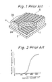
- a double insulation type (or three-layer structure) thin film EL element is formed in the following way.
- band-like transparent electrodes 2 are disposed in parallel to each other on a glass substrate 1.
- a dielectric material 3a such as Y2O3, Si3N4, Al2o3, etc.
- an EL material 4 composed or ZnS to which an active agent such as Mn, etc. is doped
- a dielectric material 3b such as Y2O3, Si3N4, TiO3, Al2O3, etc. likewise as above are laminated in turn to a film thickness of 500 -10000 ⁇ by using a thin-film technique such as vacuum deposition or sputtering to make a three-layer structure.
- band-like back electrodes 5 composed of Al (aluminum) are disposed in parallel to each other in the direction at right angles to the transparent electrode 2.
- the EL material 4 sandwiched by dielectric materials 3a, 3b is disposed between the electrodes. So, it can be regarded as a capacitive element in terms of an equivalent circuit.
- this thin-film EL element is driven by applying a relatively high voltage of about 200V.
- This thin-film EL element has characteristics that it emits highly bright light by an ac field, and yet its service life is long.
- the following method is generally used as a suitable method for keeping the display quality of a thin-film EL element which is ac driven.
- One of either the transparent electrode 2 or the back electrode 5 is made to serve as a data side electrode, and the other is made to serve as a scanning side electrode.
- a gradation voltage is applied to the data side electrode according to gradation display data on the one hand.
- a writing voltage is applied to the scanning side electrode in the order of line. And the writing voltage completes a display of one frame in a first field that serves as one of the polarities to the data side electrode and a second field that serves as the other electrode.
- This driving method causes a superposing or offset effect of the writing voltage and a modulation voltage to occur at each picture element corresponding to a intersecting position of the data side electrode and the scanning side electrode among the above EL layers 4.
- the voltage substantially applied to the picture elements becomes more than a light emission threshold voltage or less than a light emission threshold voltage. This causes each picture element to show a state of light emission or non-light emission, and a predetermined display is obtained.
- a pulse width modulation method by which the pulse width of a modulation voltage applied to a data side electrode is changed according to gradation display data, or an amplitude modulation method by which the amplitude of a modulation voltage is changed according to gradation display data, is adopted.
- a modulation voltage of the pulse width corresponding to the gradation to be displayed to the data side electrode, and a voltage of a waveform to which the amplitude of a modulation voltage is superposed to the absolute value of the amplitude of a writing voltage is applied to a picture element.
- the section corresponding to the pulse width of a modulation voltage is one that exceeds a light emission threshold voltage. That is, the area of a voltage (intensity) applied to a picture element increases as the pulse width of a modulation voltage becomes longer, and decreases as it becomes shorter.
- a modulation voltage of a pulse width opposite to the gradation to be displayed (short pulse width for a highly bright gradation, long pulse width for a low bright gradation) is applied to the data side electrode, and a voltage of the waveform in which the amplitude of the writing voltage is subtracted by the amplitude of a modulation voltage, is applied to a picture element. Therefore, the section that the pulse width of the writing voltage is subtracted by the pulse width of a modulation voltage, is one that exceeds a light emission threshold voltage. That is, the area of a voltage (intensity) applied to a picture element decreases as the pulse width of a modulation voltage becomes longer, and increases as it becomes shorter.
- gradation display data must be set opposite in the cases of negative driving and positive driving. This also applies to the case of a amplitude modulation method for a modulation voltage.
- An objective of the present invention is to provide a method and apparatus for driving a display device capable of having a function that converts a corresponding relation between gradation to be display and gradation display data depending on whether it is negative driving or positive driving without destroying the wide use of peripheral circuits and peripheral devices or complicating a driving circuit.
- the invention provides a method for driving a display device formed by interposing a dielectric layer between a plurality of scanning side electrodes and a plurality of data side electrodes, characterized in that a positive writing voltage is applied to each of scanning side electrodes in one of a pair of fields, a negative voltage is applied in the other field, a modulation voltage is applied to each of data side electrodes for the duration corresponding to the logical value of a binary code of a plurality of bits predetermined in one field, and a modulation voltage applied for the duration corresponding to the logical value of a code obtained by inverting the above binary code in the other field.
- the invention provides a method for driving a display device in which a dielectric layer is interposed between a plurality of scanning side electrodes and a plurality of data side electrodes arranged in the direction for them intersecting, to each other, a modulation voltage in which a pulse width or amplitude is changed according to the gradation display data, is applied to the data side electrodes, and a positive or negative writing voltage is applied in a line order to the scanning side electrodes to cause the picture element made of the above dielectric layer to perform a gradation display that is different in brightness in several steps, characterized in that binary coded signals corresponding to each gradation of the gradation display are used as the gradation display data, the binary coded signals are inverted so that common gradation display is made possible for one gradation display data on the basis of the logical value of the binary coded signal regardless of whether the writing voltage is negative or positive.
- binary coded signals corresponding to each gradation of gradation display are used as gradation display data.
- the logical value of the binary coded signal is applied as it is in the case of, for example, negative driving in which the writing voltage is negative, and in the case of positive driving in which the writing voltage is positive, the binary coded signals are inverted for use.
- the relation of gradation display data to gradation is reverse in the cases of negative driving and positive driving. Therefore, gradation display common to one binary coded signal is performed in both the negative and positive driving.
- gradation display common to both the negative and positive driving can be performed for one binary coded signal by using binary coded signals corresponding to each gradation of the gradation display as gradation display data to invert the logical value of the binary coded signals according to the polarity of the writing voltage. Therefore, a function that converts the correspondence relation between gradation to be display and display data depending on negative driving or positive driving can be incorporated by adding a simple circuit only without destroying the wide use of peripheral circuits or peripheral devices, or complicating a driving circuit.
- the invention provides a driving apparatus for a display device, including; a display device formed by interposing a dielectric layer between a plurality of scanning electrodes and a plurality of data electrodes, a scanning electrode circuit that applies a positive writing voltage in one field of a pair of fields, and applies a negative writing voltage in the other field to each scanning electrode, and a data electrode driving circuit that applies a modulation voltage for the duration corresponding to the logical value of a binary code of a plurality of predetermined bits in one field, and that applies a modulation voltage for the duration corresponding to the logical value of a code obtained by inverting the binary code in the other field.
- the invention provides a driving apparatus for a display device, including: the data conversion circuit that outputs binary coded data representing a gradation as it is in one of the fields and that inverts and outputs it in the other field in correspondence to each data electrode for each scanning section, a counter that performs pulse counting operation for each scanning section for each scanning electrode, a comparator that compares the binary coded data representing the gradation with the counting value output by the counter and determines the duration of a modulation voltage to be applied, and a driving device that forms a modulation voltage waveform in response to the output of the comparator and provides it to the data electrodes.
- the invention provides a driving apparatus for a display device, characterized in that a modulation voltage such that it is superposed to a predetermined display threshold voltage within the range gradation changes depending on a voltage for 100% lighting or 0% lighting, is provided to the data electrodes.
- the invention provides a method for driving a display device, including: a display device formed by interposing a dielectric layer between a plurality of scanning side electrodes and a plurality of data side electrodes, characterized in that a positive writing voltage and a negative writing voltage are applied in turn to the scanning side electrodes adjacent in one field, a modulation voltage is applied for the duration corresponding to the logical value of a binary code of a plurality of predetermined bits in the term corresponding to one electrode of the adjacent scanning side electrodes and a modulation voltage is applied for the duration corresponding to the logical value of a code obtained by inverting the binary code in the term corresponding to other electrode of the adjacent scanning side electrodes to the data side electrodes.
- the inventor further provides a driving apparatus for a display device, comprising: a display device formed by interposing a dielectric layer between a plurality of scanning side electrodes and a plurality of data side electrodes, a scanning electrode driving circuit for applying a positive writing voltage and a negative writing voltage in turn to the scanning side electrode adjacent in one field, and a data electrode driving circuit for applying a modulation voltage for the duration corresponding to the logical value of a binary code of a plurality of predetermined bits in the term corresponding to one electrode of the adjacent scanning side electrode and applying a modulation voltage for the duration corresponding to the logical value of a code obtained by inverting the binary code in the term corresponding to other electrode of the adjacent scanning side electrodes to the data side electrodes.
- the invention provides a method for driving a display device, including: a display device formed by interposing a dielectric layer between a plurality of scanning side electrodes and a plurality of data side electrodes, characterized in that positive writing voltage and negative writing voltage are applied in turn to the scanning side electrode adjacent in one field of two fields which form a pair, and negative writing voltage and positive writing voltage are applied in turn to the scanning side electrode adjacent in the other field to the scanning side electrodes, and a modulation voltage is applied for the duration corresponding to the logical value of a plurality of predetermined bits in the term for which the writing voltage of one polarity of the positive voltage and the negative voltage is applied to the scanning electrodes and a modulation voltage is applied for the duration corresponding to the logical value of a code obtained by inverting the binary code in the term for which the writing voltage of the other polarity is applied to the scanning electrodes to the data side electrode.
- the invention still further provides a driving apparatus for a display device, comprising: a display device formed by interposing a dielectric layer between a plurality of scanning side electrodes and a plurality of data side electrodes, a scanning electrode driving circuit for applying positive writing voltage and negative writing voltage in turn to the scanning electrode adjacent in one field of two fields which form a pair and applying negative writing voltage and positive voltage in turn to the scanning electrode adjacent in the other field to the scanning side electrodes, and data electrode driving circuit for applying a modulation voltage for the duration corresponding to the logical value of a plurality of predetermined bits in the term for which the writing voltage of one polarity of the positive voltage and the negative voltage is applied to the scanning side electrode and applying a modulation voltage for the duration corresponding to the logical value of a code obtained by inverting the binary code in the term for which the writing voltage of the other polarity is applied to the scanning side electrode to the data side electrode.
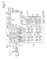
- FIG. 3 is a block diagram showing a schematic arrangement of a thin-film EL display device to which a driving method of one embodiment of the invention applies.
- a display panel 6 is composed of thin-film EL elements. Its specific arrangement is the same as for the arrangement described for the prior art. So, description thereof is omitted here.
- a plurality of scanning side electrodes Y1, Y2, --, Ym-1, Ym (hereinafter, any scanning side electrodes are denoted by the symbol Y) arranged in the display panel 6 are connected to a scanning electrode driving circuit 7.
- a plurality of scanning side electrodes X1, X2, --, Xm-1, Xm (hereinafter, any data side electrodes are denoted by the symbol X) arranged in the direction at right angles to the scanning side electrodes Y1 - Ym, are connected to a data side electrode driving circuit 8.
- output ports 9 are each connected to each of scanning side electrodes Y1 - Ym.
- a negative writing voltage -V N is selectively applied in a first field of negative driving from a power supply 10a via the output port 9.
- a positive writing voltage +V p is selectively applied to each of scanning side electrodes Y1 -Ym from another power supply 10b via the output port 9.
- These output ports 9 are connected to a shift register 11.
- Scanning data S-DATA for specifying the scanning side electrodes Y1 - Ym in a line order is transferred to the shift register 11 in synchronization with a clock CLK3 input from the clock input terminal of the shift register 11, thereby turning on each output port 9 in the line order of the scanning side electrodes Y1 - Ym.
- an output port 12 which is a driving circuit, is connected to each of data side electrodes X1 - Xn, and the modulation voltage V M is selectively applied to each of data side electrodes X1 - Xn from a power supply 13 via thin output port 12.
- V M modulation voltage
- each of data side electrodes X1 - Xn is clamped to the ground.
- These output ports 12 are connected to a comparator 14.
- This comparator 14 is connected to a shift register 16 via a latch circuit 15.
- the shift register 16 is a circuit for shifting in synchronization with the clock CLK1 input from its clock input terminal and transferring gradation display data of 4 bits that correspond to the data side electrode X1 - Xn.
- the gradation display data transferred by the shift register 16 is temporarily held in the latch circuit 15 by the latch signal LE, after which it is sent to the comparator 14.
- the comparator 14 has a function that determines the pulse width of a modulation voltage V M corresponding to gradation display data by comparing 4-bit parallel data provided from the counter 17 with the similarly 4-bit gradation display data provided from the latch circuit 15.
- a data conversion circuit 18 is a circuit for converting gradation display data sent from a data output circuit 20 as a 4-bit binary coded signal according to the negative driving time or positive driving time, and providing the converted gradation display data to the shift register 16.
- the binary coded signals sent to this circuit 18 as gradation display data are defined as shown in Table 1 in correspondence with brightness levels of 16 steps to be displayed in a picture element. In FIG. 3, each picture element in the display panel 6 is equivalently shown by a capacitor.
- FIG. 4 is a circuit diagram showing a specific arrangement of the data conversion circuit 18.
- input terminals IP0, IP1, IP2, and IP3 are terminals for inputting bits in each place of binary coded signals provided as gradation display data from a data output circuit 20.
- the input terminals IP0, IP1, IP2, and IP3 are respectively connected to one of the input terminals of a first EX-OR (exclusive logical AND) gate 19a, one of the input terminals of a second EX-OR gate 19b, one of the input terminals of a third EX-OR gate 19c, and one of the input terminals of a fourth EX-OR gate 19d.
- EX-OR exclusive logical AND
- each of EX-OR gates 19a - 19d is connected to the input terminal IP that accepts the field switching signal N/P that becomes low in the first field of negative driving and becomes high in the second field of positive driving.
- the output terminals OP0, OP1, OP2 and OP3 of each of EX-OR gates 19a - 19d are connected to the shift register 16.
- FIG. 3 A basic operation of a thin-film EL display device shown in FIG. 3 will now be described with reference to a timing chart shown in FIG. 5.
- converted 4-bit gradation display data sent from the data conversion circuit 18 is transferred in synchronization with the clock CLK1.
- This gradation display data is temporarily held in the latch circuit 15.
- the output ports 12 of the data side electrode X1 are clamped to the ground at the same time the clear signal CLR is released, and the modulation voltage V M from the output ports 12 becomes a waveform as shown in FIG. 5 (3). That is, the pulse width is set to zero.
- the count value of the clock CLK2 (see FIG. 5 (2)) counted by the counter 17 is compared with the display data "2" in the comparator 14. It is clamped to the ground at the time t2 when the count value became "2", and the modulation voltage V M of the pulse width shown in FIG. 3 (4) is set.
- the output ports 12 of the data side electrode Xn-1 are clamped to the ground at the time t4 when the count value of the counter 16 became "4", and the modulation voltage V M of the pulse width shown in FIG. 5 (5) is set.
- the modulation voltage V M of the pulse width shown in FIG. 5 (6) is set. Accordingly, the modulation voltage V M of the pulse width corresponding to gradation display data "0", "2", "4" and "7" is applied to each of data side electrodes X1, X2, Xn-1, and Xn.
- a negative writing voltage -V M or a positive writing voltage V P is applied to the one scanning side electrode Y that corresponds to the output port.
- a writing voltage -V M is applied in the first field of negative driving
- a writing voltage +V p is applied in the second field of positive driving.
- a binary coded signal "1, 0, 1, 1" equivalent to the brightness level “11" shown in table 1 is input to the data conversion circuit 18, then a high-level signal is input to the input terminals IP0, IP1, and IP3, and a low-level signal is input to the input terminal IP2. Since the field switching signal N/P input to the input terminal IP is low in the first field of negative driving, data input to the input terminals IP0 -IP3 are output as it is to the output terminals OP0 - OP3 of each of the EX-OR gates 19a - 19d. That is, the gradation display data "1, 0, 1, 1" input to the data conversion circuit 18 is sent to the shift register without modifications.
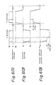
- FIG. 6 shows the waveform of the voltage applied to a corresponding picture element at this time.
- FIG. 6 (1) shows a waveform of a modulation voltage V M applied from the data side electrode X.
- FIG. 6 (2) shows the waveform of a writing voltage -V M , +V p applied from the scanning side electrode Y.
- FIG. 6 (3) shows the waveform of a voltage applied to a picture element.
- a modulation voltage V M of the pulse width equivalent to the gradation display data "1, 0, 1, 1" (brightness level “11") at the time of input to the data conversion circuit 18 is set. Since the writing voltage at this time is a negative voltage -V M as shown in FIG. 6 (2), the section corresponding to the pulse width of the modulation voltage V M becomes the section in which the writing voltage exceeds the light emission threshold voltage -Vth, and the brightness level "11" corresponding to the pulse width of the modulation voltage V M is displayed as it is.
- a modulation voltage V M of the pulse width equivalent to the gradation display data "0, 1, 0, 0" (brightness level “4") obtained by inverting the logical value of the gradation display data "1, 0, 1, 1" (brightness level "11") at the time of input to the data conversion circuit 18 is set. Since the writing voltage at this time is a positive voltage +V p as shown in FIG. 6 (2), in the waveform of the voltage shown in FIG.
- a brightness level "11" is displayed. That is, in both the negative driving and positive driving, a common brightness level corresponding to the gradation display data input to the data conversion circuit 18 is displayed.
- the data conversion circuit 18 is incorporated in the data electrode driving circuit 8 is shown.
- the data circuit 18 may be arranged separately from the data electrode driving circuit 8.
- the scanning electrodes Y may be applied with voltages in such a way that, for example, a positive writing voltage +V p is applied to the odd-numbered scanning electrodes Y1, Y3 --- in one of the fields (first field), and a negative writing voltage +V N is applied to the even-numbered scanning electrodes Y2, Y4 ---.
- a negative writing voltage -V N is applied to the odd-numbered scanning electrodes Y1, Y3 ---
- a positive writing voltage +V p is applied to the even-numbered scanning electrodes Y2, Y4 ---.
Landscapes
- Engineering & Computer Science (AREA)
- Multimedia (AREA)
- Signal Processing (AREA)
- Chemical & Material Sciences (AREA)
- Crystallography & Structural Chemistry (AREA)
- Physics & Mathematics (AREA)
- Computer Hardware Design (AREA)
- General Physics & Mathematics (AREA)
- Theoretical Computer Science (AREA)
- Control Of El Displays (AREA)
- Control Of Indicators Other Than Cathode Ray Tubes (AREA)
- Electroluminescent Light Sources (AREA)
Applications Claiming Priority (2)
| Application Number | Priority Date | Filing Date | Title |
|---|---|---|---|
| JP63304956A JP2619028B2 (ja) | 1988-11-30 | 1988-11-30 | 表示装置の駆動方法および装置 |
| JP304956/88 | 1988-11-30 |
Publications (2)
| Publication Number | Publication Date |
|---|---|
| EP0372364A1 true EP0372364A1 (de) | 1990-06-13 |
| EP0372364B1 EP0372364B1 (de) | 1994-04-06 |
Family
ID=17939338
Family Applications (1)
| Application Number | Title | Priority Date | Filing Date |
|---|---|---|---|
| EP89121980A Expired - Lifetime EP0372364B1 (de) | 1988-11-30 | 1989-11-29 | Verfahren und Vorrichtung zum Betrieb einer Anzeige |
Country Status (4)
| Country | Link |
|---|---|
| US (1) | US6127993A (de) |
| EP (1) | EP0372364B1 (de) |
| JP (1) | JP2619028B2 (de) |
| DE (1) | DE68914415T2 (de) |
Cited By (3)
| Publication number | Priority date | Publication date | Assignee | Title |
|---|---|---|---|---|
| GB2336459A (en) * | 1998-04-13 | 1999-10-20 | Fuji Electric Co Ltd | Displaying images with gradations on a matrix-type display device |
| EP1253576A2 (de) * | 2001-04-25 | 2002-10-30 | Lg Electronics Inc. | Verfahren zur Ansteuerung einer Anzeigetafel |
| EP1148466A3 (de) * | 2000-04-18 | 2009-10-14 | Semiconductor Energy Laboratory Co., Ltd. | Organische elektrolumineszierende Anzeigevorrichtung |
Families Citing this family (6)
| Publication number | Priority date | Publication date | Assignee | Title |
|---|---|---|---|---|
| JPH0960591A (ja) * | 1995-08-21 | 1997-03-04 | Toyota Autom Loom Works Ltd | 圧縮機のオイル分離機構 |
| TW502236B (en) * | 2000-06-06 | 2002-09-11 | Semiconductor Energy Lab | Display device |
| JP3749147B2 (ja) * | 2001-07-27 | 2006-02-22 | シャープ株式会社 | 表示装置 |
| KR20060104223A (ko) * | 2005-03-29 | 2006-10-09 | 삼성에스디아이 주식회사 | 전자방출소자의 구동장치 및 그 구동 방법 |
| KR20060112474A (ko) * | 2005-04-27 | 2006-11-01 | 삼성전자주식회사 | 표시 장치 및 그 구동 방법 |
| US8004482B2 (en) * | 2005-10-14 | 2011-08-23 | Lg Display Co., Ltd. | Apparatus for driving liquid crystal display device by mixing analog and modulated data voltage |
Citations (5)
| Publication number | Priority date | Publication date | Assignee | Title |
|---|---|---|---|---|
| EP0051521A1 (de) * | 1980-10-27 | 1982-05-12 | Commissariat à l'Energie Atomique | Verfahren zum Steuern einer optischen Charakteristik eines Materials |
| FR2505072A1 (fr) * | 1981-04-22 | 1982-11-05 | Lohja Ab Oy | Procede de commande d'affichage d'image, en particulier d'affichage electroluminescent en courant alternatif |
| EP0201369A1 (de) * | 1985-04-04 | 1986-11-12 | Commissariat A L'energie Atomique | Verfahren zur Steuerung einer Graustufen anzeigenden Matrixanzeigeanordnung |
| GB2177831A (en) * | 1985-07-12 | 1987-01-28 | Sharp Kk | Display device |
| GB2186414A (en) * | 1986-02-06 | 1987-08-12 | Seiko Epson Corp | Liquid crystal display device and method of driving same |
Family Cites Families (8)
| Publication number | Priority date | Publication date | Assignee | Title |
|---|---|---|---|---|
| JPS5437800B2 (de) * | 1973-06-19 | 1979-11-16 | ||
| JPS5450289A (en) * | 1977-09-27 | 1979-04-20 | Sharp Corp | Multi-gradation image display device |
| JPS5467330A (en) * | 1977-11-09 | 1979-05-30 | Hitachi Ltd | Display unit |
| DE3026392C2 (de) * | 1980-02-26 | 1985-08-22 | Sharp K.K., Osaka | Anzeigevorrichtung mit einem elektrolumineszenten Dünnschichtelement zur Bilddarstellung |
| US4594589A (en) * | 1981-08-31 | 1986-06-10 | Sharp Kabushiki Kaisha | Method and circuit for driving electroluminescent display panels with a stepwise driving voltage |
| US4733228A (en) * | 1985-07-31 | 1988-03-22 | Planar Systems, Inc. | Transformer-coupled drive network for a TFEL panel |
| US4742346A (en) * | 1986-12-19 | 1988-05-03 | Rca Corporation | System for applying grey scale codes to the pixels of a display device |
| JPH0748137B2 (ja) * | 1987-07-07 | 1995-05-24 | シャープ株式会社 | 薄膜el表示装置の駆動方法 |
-
1988
- 1988-11-30 JP JP63304956A patent/JP2619028B2/ja not_active Expired - Lifetime
-
1989
- 1989-11-29 DE DE68914415T patent/DE68914415T2/de not_active Expired - Lifetime
- 1989-11-29 EP EP89121980A patent/EP0372364B1/de not_active Expired - Lifetime
-
1992
- 1992-03-31 US US07/860,254 patent/US6127993A/en not_active Expired - Lifetime
Patent Citations (5)
| Publication number | Priority date | Publication date | Assignee | Title |
|---|---|---|---|---|
| EP0051521A1 (de) * | 1980-10-27 | 1982-05-12 | Commissariat à l'Energie Atomique | Verfahren zum Steuern einer optischen Charakteristik eines Materials |
| FR2505072A1 (fr) * | 1981-04-22 | 1982-11-05 | Lohja Ab Oy | Procede de commande d'affichage d'image, en particulier d'affichage electroluminescent en courant alternatif |
| EP0201369A1 (de) * | 1985-04-04 | 1986-11-12 | Commissariat A L'energie Atomique | Verfahren zur Steuerung einer Graustufen anzeigenden Matrixanzeigeanordnung |
| GB2177831A (en) * | 1985-07-12 | 1987-01-28 | Sharp Kk | Display device |
| GB2186414A (en) * | 1986-02-06 | 1987-08-12 | Seiko Epson Corp | Liquid crystal display device and method of driving same |
Cited By (12)
| Publication number | Priority date | Publication date | Assignee | Title |
|---|---|---|---|---|
| GB2336459A (en) * | 1998-04-13 | 1999-10-20 | Fuji Electric Co Ltd | Displaying images with gradations on a matrix-type display device |
| EP1148466A3 (de) * | 2000-04-18 | 2009-10-14 | Semiconductor Energy Laboratory Co., Ltd. | Organische elektrolumineszierende Anzeigevorrichtung |
| US7623099B2 (en) | 2000-04-18 | 2009-11-24 | Semiconductor Energy Laboratory Co., Ltd. | Display device |
| US7623100B2 (en) | 2000-04-18 | 2009-11-24 | Semiconductor Energy Laboratory Co., Ltd. | Display device |
| US7623098B2 (en) | 2000-04-18 | 2009-11-24 | Semiconductor Energy Laboratory Co., Ltd. | Display device |
| US7990348B2 (en) | 2000-04-18 | 2011-08-02 | Semiconductor Energy Laboratory Co., Ltd. | Display device |
| US8194008B2 (en) | 2000-04-18 | 2012-06-05 | Semiconductor Energy Laboratory Co., Ltd. | Display device |
| US8400379B2 (en) | 2000-04-18 | 2013-03-19 | Semiconductor Energy Laboratory Co., Ltd. | Display device |
| US8638278B2 (en) | 2000-04-18 | 2014-01-28 | Semiconductor Energy Laboratory Co., Ltd. | Display device |
| US9196663B2 (en) | 2000-04-18 | 2015-11-24 | Semiconductor Energy Laboratory Co., Ltd. | Display device |
| EP1253576A2 (de) * | 2001-04-25 | 2002-10-30 | Lg Electronics Inc. | Verfahren zur Ansteuerung einer Anzeigetafel |
| US7230590B2 (en) | 2001-04-25 | 2007-06-12 | Lg Electronics Inc. | Method and apparatus for driving display panel using pulse width modulation |
Also Published As
| Publication number | Publication date |
|---|---|
| DE68914415D1 (de) | 1994-05-11 |
| JP2619028B2 (ja) | 1997-06-11 |
| JPH02149889A (ja) | 1990-06-08 |
| DE68914415T2 (de) | 1994-10-27 |
| EP0372364B1 (de) | 1994-04-06 |
| US6127993A (en) | 2000-10-03 |
Similar Documents
| Publication | Publication Date | Title |
|---|---|---|
| US5006838A (en) | Thin film EL display panel drive circuit | |
| US4554539A (en) | Driver circuit for an electroluminescent matrix-addressed display | |
| US4686426A (en) | Thin-film EL display panel drive circuit with voltage compensation | |
| EP0236767B1 (de) | Steuergerät | |
| EP0345399A2 (de) | Verfahren und Einrichtung zum Steuern eines kapazitiven Anzeigegeräts | |
| EP0489459B1 (de) | Verfahren zum Steuern einer Matrixanzeige und eine durch dieses Verfahren gesteuerte Matrixanzeige | |
| JPS63113497A (ja) | 表示装置の動作方法および表示装置 | |
| US6127993A (en) | Method and apparatus for driving display device | |
| US5206631A (en) | Method and apparatus for driving a capacitive flat matrix display panel | |
| US5999150A (en) | Electroluminescent display having reversible voltage polarity | |
| US5786797A (en) | Increased brightness drive system for an electroluminescent display panel | |
| US5151690A (en) | Method and apparatus for driving a liquid crystal display panel | |
| KR0123910B1 (ko) | 표시장치의 구동회로 | |
| KR100480857B1 (ko) | 구동 회로 및 화상 표시 장치 | |
| JPS5823090A (ja) | 表示装置 | |
| JPH07281641A (ja) | アクティブマトリクス型液晶ディスプレイ | |
| US4295137A (en) | Electroluminescent display driver system for thin-film electroluminescent devices requiring electric field reversal | |
| JP2854620B2 (ja) | 表示装置の駆動方法 | |
| JPH0748143B2 (ja) | 表示装置の駆動方法 | |
| US5032829A (en) | Thin film el display device | |
| JPH05297833A (ja) | 表示装置駆動回路 | |
| JP2892540B2 (ja) | 表示装置の駆動装置 | |
| JP2619083B2 (ja) | 表示装置の駆動方法 | |
| JP2533945B2 (ja) | 薄膜el表示装置の駆動方法 | |
| JP2628760B2 (ja) | 表示装置の駆動装置 |
Legal Events
| Date | Code | Title | Description |
|---|---|---|---|
| PUAI | Public reference made under article 153(3) epc to a published international application that has entered the european phase |
Free format text: ORIGINAL CODE: 0009012 |
|
| 17P | Request for examination filed |
Effective date: 19891129 |
|
| AK | Designated contracting states |
Kind code of ref document: A1 Designated state(s): DE GB |
|
| 17Q | First examination report despatched |
Effective date: 19920527 |
|
| GRAA | (expected) grant |
Free format text: ORIGINAL CODE: 0009210 |
|
| AK | Designated contracting states |
Kind code of ref document: B1 Designated state(s): DE GB |
|
| REF | Corresponds to: |
Ref document number: 68914415 Country of ref document: DE Date of ref document: 19940511 |
|
| PLBE | No opposition filed within time limit |
Free format text: ORIGINAL CODE: 0009261 |
|
| STAA | Information on the status of an ep patent application or granted ep patent |
Free format text: STATUS: NO OPPOSITION FILED WITHIN TIME LIMIT |
|
| 26N | No opposition filed | ||
| REG | Reference to a national code |
Ref country code: GB Ref legal event code: IF02 |
|
| PGFP | Annual fee paid to national office [announced via postgrant information from national office to epo] |
Ref country code: DE Payment date: 20081127 Year of fee payment: 20 |
|
| PGFP | Annual fee paid to national office [announced via postgrant information from national office to epo] |
Ref country code: GB Payment date: 20081126 Year of fee payment: 20 |
|
| REG | Reference to a national code |
Ref country code: GB Ref legal event code: PE20 Expiry date: 20091128 |
|
| PG25 | Lapsed in a contracting state [announced via postgrant information from national office to epo] |
Ref country code: GB Free format text: LAPSE BECAUSE OF EXPIRATION OF PROTECTION Effective date: 20091128 |