EP0372808A1 - Verfahren zur Herstellung einer supraleintenden Dünnenschicht des Perovskit-Typs - Google Patents
Verfahren zur Herstellung einer supraleintenden Dünnenschicht des Perovskit-Typs Download PDFInfo
- Publication number
- EP0372808A1 EP0372808A1 EP89312400A EP89312400A EP0372808A1 EP 0372808 A1 EP0372808 A1 EP 0372808A1 EP 89312400 A EP89312400 A EP 89312400A EP 89312400 A EP89312400 A EP 89312400A EP 0372808 A1 EP0372808 A1 EP 0372808A1
- Authority
- EP
- European Patent Office
- Prior art keywords
- film
- stack
- superconductor
- films
- process according
- Prior art date
- Legal status (The legal status is an assumption and is not a legal conclusion. Google has not performed a legal analysis and makes no representation as to the accuracy of the status listed.)
- Granted
Links
Images


Classifications
-
- H—ELECTRICITY
- H10—SEMICONDUCTOR DEVICES; ELECTRIC SOLID-STATE DEVICES NOT OTHERWISE PROVIDED FOR
- H10N—ELECTRIC SOLID-STATE DEVICES NOT OTHERWISE PROVIDED FOR
- H10N60/00—Superconducting devices
- H10N60/01—Manufacture or treatment
- H10N60/0268—Manufacture or treatment of devices comprising copper oxide
- H10N60/0296—Processes for depositing or forming copper oxide superconductor layers
-
- C—CHEMISTRY; METALLURGY
- C04—CEMENTS; CONCRETE; ARTIFICIAL STONE; CERAMICS; REFRACTORIES
- C04B—LIME, MAGNESIA; SLAG; CEMENTS; COMPOSITIONS THEREOF, e.g. MORTARS, CONCRETE OR LIKE BUILDING MATERIALS; ARTIFICIAL STONE; CERAMICS; REFRACTORIES; TREATMENT OF NATURAL STONE
- C04B35/00—Shaped ceramic products characterised by their composition; Ceramics compositions; Processing powders of inorganic compounds preparatory to the manufacturing of ceramic products
- C04B35/01—Shaped ceramic products characterised by their composition; Ceramics compositions; Processing powders of inorganic compounds preparatory to the manufacturing of ceramic products based on oxide ceramics
- C04B35/45—Shaped ceramic products characterised by their composition; Ceramics compositions; Processing powders of inorganic compounds preparatory to the manufacturing of ceramic products based on oxide ceramics based on copper oxide or solid solutions thereof with other oxides
-
- H—ELECTRICITY
- H10—SEMICONDUCTOR DEVICES; ELECTRIC SOLID-STATE DEVICES NOT OTHERWISE PROVIDED FOR
- H10N—ELECTRIC SOLID-STATE DEVICES NOT OTHERWISE PROVIDED FOR
- H10N60/00—Superconducting devices
- H10N60/80—Constructional details
- H10N60/85—Superconducting active materials
- H10N60/855—Ceramic superconductors
- H10N60/857—Ceramic superconductors comprising copper oxide
-
- Y—GENERAL TAGGING OF NEW TECHNOLOGICAL DEVELOPMENTS; GENERAL TAGGING OF CROSS-SECTIONAL TECHNOLOGIES SPANNING OVER SEVERAL SECTIONS OF THE IPC; TECHNICAL SUBJECTS COVERED BY FORMER USPC CROSS-REFERENCE ART COLLECTIONS [XRACs] AND DIGESTS
- Y10—TECHNICAL SUBJECTS COVERED BY FORMER USPC
- Y10S—TECHNICAL SUBJECTS COVERED BY FORMER USPC CROSS-REFERENCE ART COLLECTIONS [XRACs] AND DIGESTS
- Y10S505/00—Superconductor technology: apparatus, material, process
- Y10S505/725—Process of making or treating high tc, above 30 k, superconducting shaped material, article, or device
- Y10S505/73—Vacuum treating or coating
- Y10S505/731—Sputter coating
-
- Y—GENERAL TAGGING OF NEW TECHNOLOGICAL DEVELOPMENTS; GENERAL TAGGING OF CROSS-SECTIONAL TECHNOLOGIES SPANNING OVER SEVERAL SECTIONS OF THE IPC; TECHNICAL SUBJECTS COVERED BY FORMER USPC CROSS-REFERENCE ART COLLECTIONS [XRACs] AND DIGESTS
- Y10—TECHNICAL SUBJECTS COVERED BY FORMER USPC
- Y10S—TECHNICAL SUBJECTS COVERED BY FORMER USPC CROSS-REFERENCE ART COLLECTIONS [XRACs] AND DIGESTS
- Y10S505/00—Superconductor technology: apparatus, material, process
- Y10S505/725—Process of making or treating high tc, above 30 k, superconducting shaped material, article, or device
- Y10S505/73—Vacuum treating or coating
- Y10S505/732—Evaporative coating with superconducting material
-
- Y—GENERAL TAGGING OF NEW TECHNOLOGICAL DEVELOPMENTS; GENERAL TAGGING OF CROSS-SECTIONAL TECHNOLOGIES SPANNING OVER SEVERAL SECTIONS OF THE IPC; TECHNICAL SUBJECTS COVERED BY FORMER USPC CROSS-REFERENCE ART COLLECTIONS [XRACs] AND DIGESTS
- Y10—TECHNICAL SUBJECTS COVERED BY FORMER USPC
- Y10S—TECHNICAL SUBJECTS COVERED BY FORMER USPC CROSS-REFERENCE ART COLLECTIONS [XRACs] AND DIGESTS
- Y10S505/00—Superconductor technology: apparatus, material, process
- Y10S505/725—Process of making or treating high tc, above 30 k, superconducting shaped material, article, or device
- Y10S505/742—Annealing
Definitions
- the present invention relates to a process for preparing a perovskite type superconductor film, particularly Bi-(Pb)-Sr-Ca-Cu-O and Tl-Ba-Ca-Cu-O systems with a high content of the high Tc phase, i.e., having a high critical temperature Tc of superconductivity.
- Known superconductors having a critical temperature Tc above 100 K are Bi-Sr-Ca-Cu-O and Tl-Ba-Ca-Cu-O systems. These Bi- and Tl- systems have the advantages of a resistance to water and oxygen degradation. Nevertheless, the Bi- and Tl-system superconductors have a disadvantage in that a low Tc phase is easily formed and the formation of a single high Tc phase is difficult.
- the Bi-system is typically a mixed phase formed of a low Tc phase with a critical temperature Tc of about 80 K and a high Tc phase with a Tc of about 110K.
- the Tl-system is typically a mixed phase formed of a low Tc phase with a critical temperature Tc of about 105 K and a high Tc phase with a Tc of about 125 K. The formation of isolated high Tc phases has not been accomplished.
- the present invention provides a process for preparing a perovskite type superconducting film, comprising the steps of: depositing at least one first film of a first material constituting a perovskite type superconductor over a substrate; depositing at least one second film of a second material containing an oxide having a vapor pressure of more than 10 ⁇ 4 Pa at 800°C at least as a main component over the substrate, thereby forming a stack of the first and second films; and heat treating the stack of the first and second films to form the perovskite type superconductor film on the substrate.
- the present invention provides a process for preparing a perovskite type superconductor film on a substrate, comprising the steps of: depositing a composite oxide film of a Bi-Sr-Ca-Cu-O system having a thickness of 50 to 2,000 nm on a substrate; optionally depositing a Bi2O3 film having a thickness of 5 to 20 nm on the first composite oxide, film at a first temperature of 200 to 500°C; depositing a PbO film having a thickness of 5 to 20 nm on the first composite oxide film at a second temperature less than 500°C; optionally depositing a CuO film having a thickness of 5 to 30 nm at a third temperature of 200 to 500°C; repeating the deposition of the composite oxide, Bi2O3 if necessary and PbO films to form a stack of the composite oxide film, the Bi2O3 film if present, the CuO film if present, and the PbO film on the substrate, the stack having a top film of the
- the present invention also provides a process for preparing a perovskite type superconductor film on a substrate, comprising the steps of: depositing a composite oxide film of a Tl-Bi-Ca-Cu-O system having a thickness of 50 to 2,000 nm on a substrate; depositing a Tl2O3 film having a thickness of 10 to 20 nm on the first composite oxide film at a first temperature of 200 to 500°C; repeating the deposition of the composite oxide and Tl2O3 films to form a stack of the composite oxide and Tl2O3 films on the substrate, the stack having a top film of the composite oxide film; and heat treating the stack at a second temperature of 750 to 890°C higher than the first temperature to form a film of a Tl-Ba-Ca-Cu-O perovskite type superconductor on the substrate.
- the present invention there is also provided an optimum composition for forming high Tc phase Bi2 Sr2 Ca2 Cu3 O x in Pb-doped Bi system thin films.
- doping with Pb enhanced the high Tc phase formation in the bulk system
- the present inventors found that in thin films, doped Pb easily evaporates during post-annealing or sintering and a larger amount of Pb is necessary to synthesize the high Tc phase.
- the present inventors optimized the Cu content in the deposited film. A slightly excess Cu effectively decreases the low Tc phase.
- a preferred composition for the as-deposited film before post-annealing is a ratio of Bi/Pb of 1/0.5-1.5, more preferably 1/0.6-0.9, and a ratio of Sr/Cu of 1.5-1.7.
- a most preferred composition is Bi:Pb:Sr:Ca:Cu of 0.8-1.1:0.5-1.0:1:0.9-1.1:1.5-1.7.
- Bi-Sr-Ca-Cu-O and Tl-Ba-Ca-Cu-O system superconductors comprise at least four metal elements, and as a result, it is difficult to adjust the composition to a desired value.
- metal elements having a relatively high vapor pressure such as Bi, Pb and Tl, tend to be lost from a deposited film, e.g., by evaporation during the deposition and annealing of the film. The extent to which the elements in the deposited film are lost depends on the substrate temperature, the deposition rate of the film and the annealing temperature. Therefore, the composition of the film is not reproducible.
- Figure 1 shows the X-ray diffraction pattern of a Bi-Sr-Ca-Cu-O film formed in accordance with the prior art.
- a sintered oxide target of Bi2Sr2Ca2Cu3O x was prepared by firing a mixture of oxides in air at 800°C for 24 hours.
- a film was deposited by RF magnetron sputtering on a MgO substrate from the above target heated to 400°C under 1 Pa, and the obtained film having a thickness of 1 ⁇ m was then heat treated at 875°C for 5 hours.
- the thus-obtained film comprised of, as seen from Fig.
- the present invention resolves the above problem by independently forming a layer containing, at least as a main component, an oxide or element having a high vapor pressure of more than 10 ⁇ 4 Pa, particularly more than 10 ⁇ 2, at 800°C, such as Bi2O3 , PbO x or Tl2O3 , in a stack of oxide layers, to have an average composition close to a desired value whereby, after heat treating the stack for a short time, a superconductor film comprising a phase having a structure containing three CuO planes in a 1/2 unit, the superconductor film having a high critical temperature and a high critical current density, is thus obtained.
- the present invention provides a process for preparing a Bi-(Pb)-Sr-Ca-Cu-O or Tl-Ba-Ca-Cu-O system superconductor film, comprising the steps of: depositing at least one first film of a first oxide constituting a perovskite type superconductor over a substrate at a first temperature; depositing at least one second film containing a second oxide having a vapor pressure of more than 10 ⁇ 4Pa at 800°C at least as a main component of the second film over the substrate, thereby forming a stack of the first and second oxide films; and heat treating the stack of the first and second oxide films at a second temperature higher than the first temperature in an atmosphere containing oxygen to form the perovskite type superconductor film on the substrate.
- At least one oxide having a vapor pressure of more than 10 ⁇ 4Pa at 800°C is independently deposited because, at said first temperature for deposition if such a high vapor pressure oxide is deposited at this temperature, and at said second temperature for said heat treatment, said oxide or the element of said oxide is easily evaporated and the composition of the film is considerably varied, and therefore a compensation, of the evaporating component is necessary, in order to obtain a high Tc phase superconductor with the stoichiometric composition.
- the perovskite type superconductor of the present invention also includes a superconductor having the above composition, Bi2(Sr 1-x Ca x ) m Cu n O z , in which a part of an element or elements thereof is replaced by Pb and/or Pb is further added.
- Such superconductors may be represented by the formula: Bi 2-y Pb r (Sr 1-x Ca x )4 Cu3O z where 0 ⁇ x ⁇ 1, y > 0, r > 0, and z > 0. Also, in the above Tl-system, a part of an element or elements thereof may be replaced by Pb.
- the oxides or elements having a vapor pressure of higher than 10 ⁇ 4pa at 800°C in the above superconductors are Bi2O3(Bi), PbO x (Pb), and Tl2O3(T1). These oxides are preferably deposited at a temperature (for example, less than 500°C) lower than a temperature (typically 750 - 890°C) of a heat treatment for forming a perovskite type superconductor.
- a preferable temperature for depositing the oxides, particularly PbO is 200 to 500°C, more preferably 350 to 400°C. At a temperature higher than 500°C, evaporation occurs, and at a temperature lower than 200°C, the adhesion of the deposited oxide film is poor.
- the film of Bi-(Pb)-Sr-Ca-Cu-O system as deposited and before the heat treatment should have an average composition with a ratio of Bi/Pb of 1/0.5 - 1.5, more preferably 1/0.6 - 0.9.
- a ratio of Bi/Pb of about 1.8/0.34 i.e., 1/0.189 is thought preferable as a starting material for forming a bulk superconductor (Kawai et al, Jpn. J. appl. Phys. 27, 1988, L1476).
- the present inventors found that Pb or PbO x in a film is preferentially and greatly evaporated during a heat treatment of the stack, and the high Tc phase is formed mainly when Pb remains in the film after deposition, and therefore, to form a high Tc phase superconductor film, Pb is necessary in an as-deposited film in an amount more than the amount adequate for bulk samples. But if too much Pb is in the as-deposited film, the film is partially fused during the heat treatment and the heat treated film phase separated.
- An excess amount of CuO is preferred because the high Tc phase is more easily formed when an excess amount of CuO is present.
- CuO may be deposited as a separate CuO film in a stack of films, as the above described element or oxide having a high vapor pressure.
- the deposition of the oxides may be performed by physical vapor deposition such as sputtering, evaporation, molecular beam epitaxy (MBE), etc., or chemical vapor deposition (CVD) including plasma CVD, etc., or other processes.
- physical vapor deposition such as sputtering, evaporation, molecular beam epitaxy (MBE), etc.
- chemical vapor deposition CVD including plasma CVD, etc., or other processes.
- Certain elements or oxides of the superconductor may be deposited together because they do not have a high vapor pressure, and therefore, can be deposited without hard evaporation even by simultaneous deposition or if desired may be separately deposited, particularly CuO.
- the thickness of the film having a low vapor pressure of the oxide or element is 50 nm to 200 nm.
- the order of the deposition of the films is preferably: first depositing an oxide having a low vapor pressure directly on a substrate so that adhesion of the film to the substrate is firm; and last depositing an oxide having a low vapor pressure as the top film of the stack to prevent evaporation of oxide or element having a high vapor pressure from the top of the stack during the heat treatment in order to form the perovskite type superconductor.
- the stack of the films may have a composition which is stepwise or gradually changed from one film to an adjacent film.
- the number of films in the stack is not limited, and a combination of a film of an oxide having a high vapor pressure and a film of an oxide having a low vapor pressure may be repeatedly stacked.
- the stack thus obtained is heat treated at a temperature higher than the temperature at which the oxide was deposited.
- a perovskite type superconductor is formed having an approximately stoichiometric composition and containing the high Tc phase at a high volume fraction.
- the amount of the oxide having a high vapor pressure may be lower than that of the as-deposited stack.
- the content of Pb is often reduced or even completely lost after the heat treatment, but a high volume fraction of the high Tc phase is obtainable.
- Pb acts as an accelerator for forming the high Tc phase and is not necessarily a component of the high Tc phase.
- a separate formation of the PbO film is an important feature of the present invention. A preferred content of the PbO in the as-deposited stack has been described.
- the temperature of the heat treatment is 835°C to 870°C. At a temperature lower than 835°C, a low Tc phase superconductor is also formed, and at a temperature higher than 870°C, the superconductor may be melted.
- an oxide of an element having a high vapor pressure and difficult to deposit or an element or oxide which is relatively easily evaporated during a post-annealing of the deposited film is independently and concentratedly deposited, and thus the time for depositing such an oxide is shortened and variations of the composition by evaporation during the deposition and the annealing of the deposited film or stack can be reduced or neglected.
- the composition of the film is very precisely controlled and a perovskite type superconductor having a high Tc and a high Jc is finally obtained.
- Figure 1 shows the X-ray diffraction pattern of the heat-treated sample. It is seen from Fig. 1 that a Bi2Sr2CuO x phase having a Tc of 10 K and a low Tc Bi2Sr2CaCu2O3 phase having a Tc of 80 K were formed.
- Figure 2 shows the X-ray diffraction pattern of the above heat treated sample. It is seen from Fig. 2 that the high Tc phase of Bi2Sr2Ca2Cu3O z was formed but the volume fraction thereof was still very low in comparison with the volume fraction of the low Tc phase of Bi2Sr2CaCu2O x .
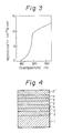
- Figure 3 shows the electric resistivity dependence on the temperature in which the on-set temperature was higher than 110 K but the Tce (end point of the critical temperature) was 75 K.
- composition of the film was determined by EPMA and it was found that Bi was lacking and the composition was non-stoichiometric, and that only a little Pb was doped in the deposited film (therefore, it is understood that the content of Pb was not enough to form a high Tc phase).
- EPMA analysis revealed that the annealed film had a composition very close to the stoichiometric composition of the high Tc phase, i.e., the content of Bi was adequately compensated.
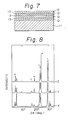
- Figure 4 illustrates the layer structure of the stack formed in this example, in which a plurality of Bi-Sr-Ca-Cu-O films 2, Bi2O3 films 3 and PbO films 4, in this order, are deposited on a MgO substrate 1 and another Bi-Sr-Ca-Cu-O film 2′ is finally deposited on the top of the stack of the films 2, 3 and 4.
- the above deposition was carried out by magnetron sputtering using the targets A, C and D.
- the thicknesses of the Bi-Sr-Ca-Cu-O film 2, the Bi2O3 film 3, and the PbO film 4 were 300 nm, 20 nm and 10 nm, respectively, and the total thickness of the stack was about 1 ⁇ m.
- the thus-obtained stack was heat treated in air at 850°C for 10 minutes to 15 hours.
- the Pb continuously evaporated during the heat treatment of the stack and only a small amount of Pb remained after 3 hours at 850°C.
- the as-deposited oxide films were amorphous, but reacted to form the high Tc phase after the heat treatment at 850°C for 10 minutes, the volume fraction of the high Tc phase in the reacted film being one third. After 1 hour, more than half of the film was high Tc phase, and after 15 hours, only a small amount of Pb remained but the film was almost entirely high Tc phase only. This suggests that Pb accelerates the formation of the high Tc phase but the formation of the high Tc phase does not always require Pb.
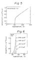
- FIG. 5 shows the electric resistivity v.s. the temperature of the thus-obtained film.
- the electric resistivity is linearly decreased with a lowering of the temperature, and rapidly decreased at around 110 K.
- the Tce of the film was 94.5 K after 10 minutes heat treatment at 850°C and 106.5 K after 1 hour heat treatment. After 15 hours heat treatment at 850°C, the Tce of the film was 105.4 K and almost the same as that after 1 hour heat treatment, but the on-set temperature was slightly elevated.
- Figure 6 shows the temperature dependence of the electric resistivity in relation to the current density. It is seen that a satisfactory characteristic was obtained 2.47 x 10³ A/cm2 at liquid nitrogen temperature.
- a plurality of targets including a sintered target (Bi2Sr2Ca2Cu3O z Bi2Pb 0.4 Sr2Ca2Cu3O z , etc.) for depositing a complex oxide containing the elements constituting the perovskite type superconductor; a compensating target (Bi2O3 , Tl2O3 , etc.) for depositing a compensating film to compensate for a component which, among the elements constituting the superconductor, has a high vapor pressure at a temperature of the film deposition or at a temperature of the heat treatment or annealing, and evaporates during the steps such that the content thereof is very low in the deposited or heat treated film; and a target of a high Tc phase formation accelerating component (PbO x , etc.) for supplying a high Tc phase formation accelerating component such as PbO x , which is not an essential component of the high Tc phase of the superconduct
- a sintered target Ba2S
- a stack of films having a structure as shown in Fig. 7 was formed on a single crystal MgO substrate by a magnetron sputtering.
- 11 denotes the substrate
- 12 a Bi-Sr-Ca-Cu-O system film having a thickness of 200 nm
- 13 a PbO film having a thickness of 20 nm.
- Atmosphere a mixed gas of Ar and O2 with a ratio of Ar/O2 of 2/1 Pressure: 1 Pa
- RF power 100 W for the Bi-Sr-Ca-Cu-O film and 75 W for the PbO x film
- Temperature of substrate 400°C
- the amount of Bi was adequate due to the high content thereof in the target.
- the ratio between Pb and Bi was 0.9:1.0, which is almost adequate.
- the stack was then heat-treated in air at 850°C for minutes.
- the stacks were formed as above and then heat treated in air at 850°C for 1 hour and 15 hours.
- Figure 9 shows the composition of the superconductor film in relation to the heat treatment time, evaluated by EPMA. Along with the time of the heat treatment, Pb is rapidly evaporated and disappears from the film in about 3 hours. On the other hand, the X-ray diffraction patterns indicate that the high Tc phase was rapidly formed at the beginning of the heat treatment, i.e., when Pb existed.
- the left side ordinate represents the composition ratio and the right side ordinate represents the X-ray diffraction intensity ratio of the high Tc phase peak (002) to the low Tc phase peak (002).
- Figure 10 shows the electric resistivities of the superconductor films X, Y, Z in relation to the temperature.
- the highest Tce was 106.5 K after a 1 hour heat treatment at 850°C.
- Figure 11 shows the X-ray diffraction patterns of the above three superconductors. It is clear that the amount of the high Tc phase was not increased by the prolongation of the heat treatment.
- Figure 12 shows the electric resistivity of the superconductor film in relation to the temperature.
- the on-set temperature is 110 K but the end point Tce is 77 K.
- a stack of films having a structure as shown in Fig. 13 was formed on a single crystal MgO substrate by magnetron sputtering.
- 21 denotes the substrate
- 22 a Bi-Sr-Ca-Cu-O system film having a thickness of 200 nm
- 23 a PbO x film having a thickness of 30 nm
- 24 a CuO film having a thickness of 30 nm.
- Atmosphere a mixed gas of Ar and O2 with a ratio of Ar/O2 of 2/1 Pressure: 1 Pa
- RF power 100 W for the Bi-Sr-Ca-Cu-O film and 75 W for the PbO x film and CuO film
- Temperature of substrate 400°C
- the amount of Bi was adequate (just the stoichiometric ratio to Sr).
- Figure 14 shows the X-ray diffraction pattern of the superconductor film. It is seen that an almost single high Tc phase of the superconductor was obtained.
- Figures 15A and 15B show microstructures of the superconductor film observed by a scanning electron microscope (SEM), in which c-axis aligned scaly superconductor crystals are seen.
- SEM scanning electron microscope
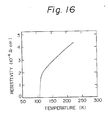
- Figure 16 shows the electric resistivity of the superconductor film in relation to the temperature. The resistance was rapidly lowered from around 106.5 K and reached zero resistivity at 106.5 K.
- the critical current density was high, 5.8 x 10⁴ A/cm2 at 77.3 K.
- Superconducting films were deposited by RF magnetron sputtering using three targets. The films were deposited on 20 x 20 mm2 MgO (100) single crystals.
- the films Bi content is usually less than the target value, and a Bi-rich target is usually used to compensate for the lack of Bi in the films.
- PbO and CuO targets were also used to dope enough Pb into the films and to optimize the Cu content.
- PbO and CuO layers were stacked repeatedly on BSCCO layers to precisely control composition. The PbO and CuO layers were several dozen nanometers thick. The total thickness of the deposited films was about 0.85 ⁇ m.
- As-deposited films were amorphous and insulating. A film was divided into about 10 x 10 mm2 samples, and one of these was analyzed by inductively coupled plasma analysis (ICP) to determine the film composition. The other films were sintered in air for 1 h at around 850°C. A muffle furnace was used and the temperature was measured by an R-type (Pt-13% Rh, Pt) thermocouple. The heating rate was 10°/min to 800°C and 1°/min above that to avoid overshooting the set temperature. During heating, the films were kept at 800°C for 20 min. The films were cooled at 10°/min. The films were examined using X-ray diffraction with a Cu K ⁇ source and a scanning electron microscope. The electrical resistivity of the films was also measured with the four-point probe method using dc current.
- ICP inductively coupled plasma analysis
- the films were doped heavily with Pb because it promoted the high Tc phase.
- As-deposited film compositions are listed in the following Table. Number 134 was Pb doped to the stoichiometric film at a ratio of 1.03 to the Sr content.
- X-ray diffraction showed that after 1 h of sintering at 852°C, large amounts of the film transformed to the high Tc phase, but about one-fourth of the film remained in the low Tc phase.
- needle-like precipitations several dozen microns long were observed with a scanning electron microscope (SEM). Heavy Pb doping deteriorates the film morphology because the film melts more easily during sintering as the Pb content increases.
- FIG. 17 shows the intensity ratios of the peaks from the high Tc phase (00 14 ) and the low Tc phase (00 12 ). Similar results are obtained from the ratios of H(002)/L(002) and H(00 10 )/L(008).
- Table Atomic compositions of Bi, Pb, Sr, Ca, and Cu determined by ICP, normalized by the Sr composition. For the upper samples, PbO target was sputtered for 8 min and for the lower, 6 min. BSCCO target was sputtered for 100 min and CuO from 15 to 24 min. Compositions Run No.
- Fig. 17 the large number indicate run number and the small numbers indicate sintering temperature. Dotted line is a guide for the eye.
- the amount of the high Tc phase depends strongly on the Cu content.
- the sintering temperature also greatly affects the amount of the high Tc phase formed.
- the low Tc phase forms below 848°C and above 853°C. This suggests that the single-phase high Tc film forms in a very narrow temperature range.
- Bi:Pb:Sr:Ca:Cu 1.00:0.80:1.00:0.99:1.64
- a nearly single-phase high Tc thin film was obtained after an hour of sintering at 851°C in air.
- the resistivity decreased linearly with temperature and had a zero resistance at 106.5 K.
- Jc reached 4.1 x 10⁴ A/cm2 at 77.3 K with a criterion of 1 ⁇ V/cm.
Landscapes
- Engineering & Computer Science (AREA)
- Chemical & Material Sciences (AREA)
- Ceramic Engineering (AREA)
- Manufacturing & Machinery (AREA)
- Materials Engineering (AREA)
- Structural Engineering (AREA)
- Organic Chemistry (AREA)
- Inorganic Compounds Of Heavy Metals (AREA)
- Superconductor Devices And Manufacturing Methods Thereof (AREA)
- Superconductors And Manufacturing Methods Therefor (AREA)
Applications Claiming Priority (8)
| Application Number | Priority Date | Filing Date | Title |
|---|---|---|---|
| JP301637/88 | 1988-11-29 | ||
| JP63301637A JP2748457B2 (ja) | 1988-11-29 | 1988-11-29 | 超伝導膜の製造方法 |
| JP1114150A JP2785038B2 (ja) | 1989-05-09 | 1989-05-09 | 超伝導体膜の製造方法 |
| JP114150/89 | 1989-05-09 | ||
| JP144503/89 | 1989-06-06 | ||
| JP144502/89 | 1989-06-06 | ||
| JP1144502A JPH0310083A (ja) | 1989-06-06 | 1989-06-06 | 超伝導膜の製造方法 |
| JP1144503A JPH038722A (ja) | 1989-06-06 | 1989-06-06 | 超電導膜の製造方法 |
Publications (2)
| Publication Number | Publication Date |
|---|---|
| EP0372808A1 true EP0372808A1 (de) | 1990-06-13 |
| EP0372808B1 EP0372808B1 (de) | 1997-08-13 |
Family
ID=27470144
Family Applications (1)
| Application Number | Title | Priority Date | Filing Date |
|---|---|---|---|
| EP89312400A Expired - Lifetime EP0372808B1 (de) | 1988-11-29 | 1989-11-29 | Verfahren zur Herstellung einer supraleitenden Dünnenschicht des Perovskit-Typs |
Country Status (5)
| Country | Link |
|---|---|
| US (2) | US5141917A (de) |
| EP (1) | EP0372808B1 (de) |
| KR (1) | KR930008648B1 (de) |
| CA (1) | CA2003850C (de) |
| DE (1) | DE68928256T2 (de) |
Families Citing this family (7)
| Publication number | Priority date | Publication date | Assignee | Title |
|---|---|---|---|---|
| US5648114A (en) * | 1991-12-13 | 1997-07-15 | Symetrix Corporation | Chemical vapor deposition process for fabricating layered superlattice materials |
| JP2625280B2 (ja) * | 1991-05-30 | 1997-07-02 | 住友電気工業株式会社 | 酸化物超電導材料の製造方法 |
| US5458086A (en) * | 1993-10-13 | 1995-10-17 | Superconductor Technologies, Inc. | Apparatus for growing metal oxides using organometallic vapor phase epitaxy |
| US5849671A (en) * | 1996-03-13 | 1998-12-15 | Industrial Research Limited | Separated reactants processing of high Tc superconductors |
| US5908813A (en) * | 1997-02-14 | 1999-06-01 | Micron Technology, Inc. | Method making integrated circuit metallization with superconductor BEOL wiring |
| CA2342376C (en) * | 2001-03-20 | 2013-11-12 | Marco Colonna | A receptor trem (triggering receptor expressed on myeloid cells) and uses thereof |
| EP1961703A4 (de) * | 2005-12-16 | 2013-05-01 | Central Res Inst Elect | Verfahren zur bildung eines dicken films aus oxidsupraleiter |
Family Cites Families (4)
| Publication number | Priority date | Publication date | Assignee | Title |
|---|---|---|---|---|
| JP2606698B2 (ja) * | 1987-03-23 | 1997-05-07 | 株式会社 半導体エネルギー研究所 | 超電導セラミツクスの作製方法 |
| JPS63241825A (ja) * | 1987-03-30 | 1988-10-07 | Fujikura Ltd | 超電導体の製造方法 |
| JPS63241824A (ja) * | 1987-03-30 | 1988-10-07 | Fujikura Ltd | 超電導体の製造方法 |
| JPS63276823A (ja) * | 1987-05-06 | 1988-11-15 | Furukawa Electric Co Ltd:The | 超電導膜の製造方法 |
-
1989
- 1989-11-24 CA CA002003850A patent/CA2003850C/en not_active Expired - Fee Related
- 1989-11-29 KR KR1019890017434A patent/KR930008648B1/ko not_active Expired - Fee Related
- 1989-11-29 EP EP89312400A patent/EP0372808B1/de not_active Expired - Lifetime
- 1989-11-29 DE DE68928256T patent/DE68928256T2/de not_active Expired - Fee Related
-
1990
- 1990-08-09 US US07/565,209 patent/US5141917A/en not_active Expired - Fee Related
-
1995
- 1995-01-25 US US08/378,087 patent/US5585332A/en not_active Expired - Fee Related
Non-Patent Citations (3)
| Title |
|---|
| APPLIED PHYSICS LETTERS, vol. 53, no. 18, 31st October 1988, pages 1759-1761, American Institute of Physics, New York, NY, US; R. RAMESH et al.: "Microstructure of Pb-modified Bi-Ca-Sr-Cu-O superconductor" * |
| CHEMICAL & ENGINEERING NEWS, vol. 66, no. 20, 16th May 1988, pages 24-29, Washington, DC, US; R. DAGANI: "New class of superconductors pushing temperatures higher" * |
| NATURE, vol. 332, 10th March 1988, page 138; Z.Z. SHENG et al.: "Bulk superconductivity at 120 K in the T1-Ca/Ba-Cu-O system" * |
Also Published As
| Publication number | Publication date |
|---|---|
| DE68928256D1 (de) | 1997-09-18 |
| KR930008648B1 (ko) | 1993-09-11 |
| KR900008707A (ko) | 1990-06-04 |
| CA2003850A1 (en) | 1990-05-29 |
| EP0372808B1 (de) | 1997-08-13 |
| DE68928256T2 (de) | 1997-12-04 |
| US5141917A (en) | 1992-08-25 |
| CA2003850C (en) | 1998-07-28 |
| US5585332A (en) | 1996-12-17 |
Similar Documents
| Publication | Publication Date | Title |
|---|---|---|
| Char et al. | Reactive magnetron sputtering of thin‐film superconductor YBa2Cu3O7− x | |
| US6226858B1 (en) | Method of manufacturing an oxide superconductor wire | |
| EP0406126B2 (de) | Substrat mit einer supraleitenden Schicht | |
| US5047385A (en) | Method of forming superconducting YBa2 Cu3 O7-x thin films with controlled crystal orientation | |
| HK87496A (en) | Method for preparing a superconducting thin film | |
| EP0446145B1 (de) | Verfahren zum Herstellen hochtemperatursupraleitender Dünnschichten | |
| EP0787363B1 (de) | Mehrschichtiger verbundwerkstoff und verfahren zu dessen herstellung | |
| EP0372808B1 (de) | Verfahren zur Herstellung einer supraleitenden Dünnenschicht des Perovskit-Typs | |
| EP0410868A2 (de) | Supraleitende Dünnschicht aus Oxid und Verfahren zu deren Herstellung | |
| Wasa et al. | Thin film processing for high-Tc superconductors of the Bi-system | |
| CA1336557C (en) | Superconducting thin film and a process for depositing the same | |
| EP0358545B1 (de) | Prozess zur Herstellung thalliumartiger supraleitender Dünnfilme | |
| Hamaguchi et al. | Metalorganic chemical vapor deposition of Tl2Ba2CaCu2O x superconducting thin films using fluorinated β‐diketonate source reagents | |
| EP0324220A1 (de) | Supraleitende Dünnschichten | |
| EP0412000B1 (de) | Verfahren zur Herstellung von supraleitenden Dünnschichten | |
| EP0344406B1 (de) | Tl-Kupferoxid-Supraleiter | |
| CA2043541C (en) | Process for preparing high-temperature superconducting thin films | |
| Fartash et al. | Solid‐state reactions in high‐temperature superconductor‐ceramic interfaces; Y‐Ba‐Cu‐O on Al2O3 versus yttria‐stabilized ZrO2, and MgO | |
| EP0357500A1 (de) | Verfahren zum Herstellen einer supraleitenden Dünnschicht vom Wismut-Typ | |
| EP0624910A1 (de) | Supraleiter und Herstellungsverfahren | |
| JPH075313B2 (ja) | 酸化物超伝導薄膜の作製方法 | |
| JP2832002B2 (ja) | Bi−Sr−Ca−Ci−O系超伝導薄膜の製造方法 | |
| JP2594271B2 (ja) | 超電導体用薄膜の製造装置および超電導体用薄膜の製造方法 | |
| EP0333513B1 (de) | Oxid-Supraleiter | |
| JPS63236794A (ja) | 酸化物超伝導薄膜の作製方法 |
Legal Events
| Date | Code | Title | Description |
|---|---|---|---|
| PUAI | Public reference made under article 153(3) epc to a published international application that has entered the european phase |
Free format text: ORIGINAL CODE: 0009012 |
|
| AK | Designated contracting states |
Kind code of ref document: A1 Designated state(s): DE FR GB |
|
| 17P | Request for examination filed |
Effective date: 19900921 |
|
| 17Q | First examination report despatched |
Effective date: 19920311 |
|
| GRAG | Despatch of communication of intention to grant |
Free format text: ORIGINAL CODE: EPIDOS AGRA |
|
| GRAH | Despatch of communication of intention to grant a patent |
Free format text: ORIGINAL CODE: EPIDOS IGRA |
|
| GRAH | Despatch of communication of intention to grant a patent |
Free format text: ORIGINAL CODE: EPIDOS IGRA |
|
| GRAA | (expected) grant |
Free format text: ORIGINAL CODE: 0009210 |
|
| AK | Designated contracting states |
Kind code of ref document: B1 Designated state(s): DE FR GB |
|
| PG25 | Lapsed in a contracting state [announced via postgrant information from national office to epo] |
Ref country code: FR Free format text: LAPSE BECAUSE OF FAILURE TO SUBMIT A TRANSLATION OF THE DESCRIPTION OR TO PAY THE FEE WITHIN THE PRESCRIBED TIME-LIMIT Effective date: 19970813 |
|
| REF | Corresponds to: |
Ref document number: 68928256 Country of ref document: DE Date of ref document: 19970918 |
|
| EN | Fr: translation not filed | ||
| PLBE | No opposition filed within time limit |
Free format text: ORIGINAL CODE: 0009261 |
|
| STAA | Information on the status of an ep patent application or granted ep patent |
Free format text: STATUS: NO OPPOSITION FILED WITHIN TIME LIMIT |
|
| 26N | No opposition filed | ||
| REG | Reference to a national code |
Ref country code: GB Ref legal event code: IF02 |
|
| PGFP | Annual fee paid to national office [announced via postgrant information from national office to epo] |
Ref country code: GB Payment date: 20021127 Year of fee payment: 14 |
|
| PGFP | Annual fee paid to national office [announced via postgrant information from national office to epo] |
Ref country code: DE Payment date: 20021205 Year of fee payment: 14 |
|
| PG25 | Lapsed in a contracting state [announced via postgrant information from national office to epo] |
Ref country code: GB Free format text: LAPSE BECAUSE OF NON-PAYMENT OF DUE FEES Effective date: 20031129 |
|
| PG25 | Lapsed in a contracting state [announced via postgrant information from national office to epo] |
Ref country code: DE Free format text: LAPSE BECAUSE OF NON-PAYMENT OF DUE FEES Effective date: 20040602 |
|
| GBPC | Gb: european patent ceased through non-payment of renewal fee |
Effective date: 20031129 |