EP0373594A2 - Rechnerspeicher mit Ausgangsleitungen, welche mittels der Speicheradresse zur Verbindung mit einem Datenbus ausgewählt werden - Google Patents
Rechnerspeicher mit Ausgangsleitungen, welche mittels der Speicheradresse zur Verbindung mit einem Datenbus ausgewählt werden Download PDFInfo
- Publication number
- EP0373594A2 EP0373594A2 EP89122924A EP89122924A EP0373594A2 EP 0373594 A2 EP0373594 A2 EP 0373594A2 EP 89122924 A EP89122924 A EP 89122924A EP 89122924 A EP89122924 A EP 89122924A EP 0373594 A2 EP0373594 A2 EP 0373594A2
- Authority
- EP
- European Patent Office
- Prior art keywords
- memory
- address
- chips
- data
- bus
- Prior art date
- Legal status (The legal status is an assumption and is not a legal conclusion. Google has not performed a legal analysis and makes no representation as to the accuracy of the status listed.)
- Granted
Links
Images


Classifications
-
- G—PHYSICS
- G06—COMPUTING OR CALCULATING; COUNTING
- G06F—ELECTRIC DIGITAL DATA PROCESSING
- G06F12/00—Accessing, addressing or allocating within memory systems or architectures
-
- G—PHYSICS
- G06—COMPUTING OR CALCULATING; COUNTING
- G06F—ELECTRIC DIGITAL DATA PROCESSING
- G06F12/00—Accessing, addressing or allocating within memory systems or architectures
- G06F12/02—Addressing or allocation; Relocation
- G06F12/06—Addressing a physical block of locations, e.g. base addressing, module addressing, memory dedication
-
- Y—GENERAL TAGGING OF NEW TECHNOLOGICAL DEVELOPMENTS; GENERAL TAGGING OF CROSS-SECTIONAL TECHNOLOGIES SPANNING OVER SEVERAL SECTIONS OF THE IPC; TECHNICAL SUBJECTS COVERED BY FORMER USPC CROSS-REFERENCE ART COLLECTIONS [XRACs] AND DIGESTS
- Y02—TECHNOLOGIES OR APPLICATIONS FOR MITIGATION OR ADAPTATION AGAINST CLIMATE CHANGE
- Y02D—CLIMATE CHANGE MITIGATION TECHNOLOGIES IN INFORMATION AND COMMUNICATION TECHNOLOGIES [ICT], I.E. INFORMATION AND COMMUNICATION TECHNOLOGIES AIMING AT THE REDUCTION OF THEIR OWN ENERGY USE
- Y02D10/00—Energy efficient computing, e.g. low power processors, power management or thermal management
Definitions
- This invention relates generally to digital computers and, more specifically, to a random access memory structure.
- a typical random access memory is formed from a plurality of integrated circuit chips.
- the chips are connected together in a manner to make connectable to a data bus at one time a number of bit locations from each of the plurality of memory chips that are at the same relative address in each chip. For example, if the data bus is 16 bits wide but the individual memory chips make only a nibble (four bits) available at its data output lines in response to a single address, four such chips are used in parallel so that four nibbles, for a total of sixteen bits, are connected to the data bus in response to the same address being applied to each of the four chips. The depth of the chips is then selected in order to provide the total memory capacity desired.
- a memory having a size of 640 kilobytes (each byte including 8 bits) is a popular standard.
- four memory chips, each one nibble wide are connected in parallel to the data bus and respond to a common address for combining their data bits together in order to form a 16-bit data word.
- the most common such chip has a total capacity of 256k deep by 4-bits wide (256,000 kilo-nibbles), four of which form a memory having a total capacity of 512 kilobytes.
- the depth of the memory is supplemented by an additional four chips of at least 64k by 4-bits in capacity, 64 kilo-nibbles being necessary from each in order to provide a memory having a depth sufficient that its total capacity is 640 kilobytes. Since the desired 64 kilo-nibble by 4 bit wide chips are not generally available, larger memory chips are often employed and the excess storage locations are simply unused. Alternatively, the memory may be made from a total of four chips that each have a larger capacity, such as four 1 megbit by 4-bit chips which are the next commercially available size after the 256k by 4-bit chips most commonly used. Excess capacity of the Meg.chips is then simply unused. In addition to increasing memory cost, the provision of unused memory capacity and/or the use of a larger number of circuit chips to form the memory increase its size and power requirements, which is undesirable in many applications, particularly in portable computers.
- data words having a width equal to that of a data bus are stored in several bit portions at different locations in various memory chips. That is, the architecture of the present invention avoids the commonly applied constraint that each portion of a data word must be stored at the same relative location of each of the chips of the memory. According to the present invention, the memory is made to be wider in terms of number oi bits than that of the data word to be simultaneously accessed. A control circuit responsive to the memory addresses selects a portion of the memory width equal to the desired data word in a manner that all of the chips are fully utilized.
- a memory having a number of chips to provide a width equal to that of the desired data word also includes at least one extra chip whose contents are selectively substituted for one of the other regular memory chips, in response to the memory address.
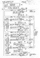
- a typical existing computer system generally includes a microprocessor 11, a read-only-memory 13, a random access memory 15, and various peripherals 17 that are all connected to a common address bus 19 and a common data bus 21.
- the address and data buses 19 and 21 are implemented as a single physical bus that is time multiplexed between address and data functions.
- Figure 2 shows an example of a R.A.M. 15 having a width of 16 bits for use on a 16-bit wide data bus, and having a total capacity of 640 kilo-bytes (655,360 bytes). This is the maximum size memory that can be addressed by a 20-bit address, and is currently the most common in personal computers.
- the 16-bit data word width is provided by four individual memory chips 23, 25, 27 and 29 connected in parallel.
- a nibble (4-bits) of the 16-bit word is stored in each of these four memory chips at the same location.
- an address bus not shown in Figure 2 connected to each of these chips, the four bits simultaneously read out from each chip are combined in parallel to form the 16-bit word.
- a common commercially available memory chip of this type has a total of 262,144 (256k) such 4-bit nibble addressable storage locations.
- the combination of the capacity of all of the four chips 23, 25, 27 and 29, is 524,288 (512k) bytes (each byte being 8-bits).
- additional memory chips 31, 33, 35 and 37 are provided as depth extensions of the individual memory chips 23, 25, 27 and 29, respectively.
- Each of the additional memory chips 31, 33, 35 and 37 need only have a capacity of 64k nibbles but since this size of memory chip is not commonly available commercially, it is often found that 256k chips are used instead.
- the excess, unused storage capacity increases the cost of the computer, consumes power and takes space.
- the width of the memory of Figure 3 is 20 bits.
- Four bits, or 1 nibble, are provided by each of the five chips 39, 41, 43, 45 and 47.
- the data word to be written into the memory or read from it at one time is only 16 bits wide, only four of those nibbles need to be accessed at any one time in order to provide a 16-bit word. In order to do so, some 16-bit words will have to have their nibbles stored at different locations among four of the five memory chips 39, 41, 43, 45 and 47.
- bits 12-15 of the data word are obtained at a location 51 of chip 47 (chip 'E') at segment '0' denoted in the table of Figure 5 as memory segment "E0".
- the data word bits 8-11 are obtained at a location 52 of memory chip 41 from memory block B3, bits 4-7 from location 53 of memory chip 43 at block C2, and bits 0-3 at location 55 in chip 45 of memory block D2.
- the particular four memory chips accessed in any one read or write operation is determined by bits 17-19 of the address, as shown in the left hand column of the Figure 5 table.
- memory chip 39 (chip 'A') is not utilized in forming the 16-bit word. But other data words, such as those having address bits 17-19 of line 4 of the Figure 5 table, utilize memory chips 39 (chip 'A'), 47 ('E'), 43 ('C'), and 45 ('D').
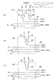
- FIG. 4 An example of a preferred implementation of the memory organization described with respect to Figure 3 is given in the circuit diagram of Figure 4.
- 16 bits of storage locations within the memory chips 39, 41, 47, 43 and 45 are connected with a data bus 59 for either reading or writing the addressed memory locations.
- the data bus 59 is formed by memory chip 39 ('A') having data lines 61 connected to bit lines 12-15 of the data bus 59.
- memory chip 41 ('B') has its four data lines 63 normally connected to bit lines 8-11 of the data bus 59.
- memory chip 43 ('C') has its four data lines 65 normally connected as bit lines 4-7 of the data bus 59
- chip 45 ('D') has its data lines connected as bit lines 0-3 of the data bus 59.
- Four data lines 69 of the fifth chip 47 are not permanently connected with any particular data bus bit lines, but rather are connected for replacing the data lines of the other four chips 39, 41, 43 and 45 in connection to the data bus 59.
- the four data lines 69 are connected to data bus bit lines 12-15 through a semiconductor switching circuit 71 that is controlled to be on or off by a control signal in a line 73.
- the data bit line 69 are connected through another such switching circuit 75, controlled by a signal in the line 76, to bit lines 8-11 of the bus 59.
- a switch 77 controlled by a signal in a control line 79 connects the four data lines 69 with data bus bit lines 4-7, and a switch 81, controlled by a signal in line 83, connects those lines to data bus bit line 0-3.
- Decoding logic 85 receives bit lines A19-A17 of the address bus 57 and has as a purpose the selection of the four memory chip blocks to be connected to the data bus 59 for any particular access. This is accomplished by placing an enabling signal on one of the control lines 73, 76, 79 or 83, or on none of these control lines, in order to set the each of the switches 71, 75, 77, and 81 into a state that selects a desired combination of four of the five memory chips for connection to the data bus 59. Simultaneously, the decoding logic generates enable signals in four of five chip enable control lines 87, 89, 91, 93 and 95. These enable lines are connected to the memory chips 39 ('A'), 41 ('B'), 43 ('C'), 45 ('D') and 47 ('E'), respectively.
- circuit 85 passively decoding the three address bit lines A19-A17.
- Five specific combinations of bit patterns in those address lines indicated in the table of Figure 5, provide five different combinations of control signals in control lines 73, 76, 79, and 83, and in chip enable lines 87, 89, 91, 93, and 95.
- the control line 83 is enabled, while the control lines 73, 76 and 79 are disabled, thereby connecting four bits addressed in memory chip 47 ('E') for those of memory chip 45 ('D') in data bus bit locations 0-3 by connection of the chip 47 to the data bus 59 through switching circuit 81. Simultaneously, all of the five chip enable lines are active but line 93 since the memory chip 45 ('D') that it controls is not accessed at this time and thus desired to be disabled.
- an enable signal is provided in control line 79 but not in any of the control lines 73, 76 and 83, while no chip enable signal occurs in line 91, which disables memory chip 43 ('C').
- line 4 of the Figure 5 table indicates a condition where the line 76 is enabled, while chip enable line 89 (chip 'B') is not.
- Line 5 of the Figure 5 table shows the final condition where line 73 is enabled and chip enable line 87 (chip 'A') is disabled.
- address translator circuits 121, 122 and 123 are provided between the system bus 57 and their respective memory chips.
- the logic circuits of these address translators are given in Figures 7(A), 7(B) and 7(C).
- the translation affects the values of only bit numbers 17 (MA17) and 18 (MA18) of the address, as shown by the table of Figure 6 and the circuits of Figure 7.
- chips 'A' and 'E' The address to the remaining two memory chips 39 and 47 (chips 'A' and 'E') is provided directly from the system bus 57, without any translation. This can be seen from the columns of the table of Figure 6 for chips 'A' and 'E', where the system address bus bit values A17 and A18 are the same, respectively, as the address bit values MA17 and MA18 applied to those two chips.
- the two bits MA17 and MA18 for the memory chip 41 are given in column 'B' of the table of Figure 6 for five combinations of the system bus address bits A17, A18 and A19.
- the circuit for accomplishing that translation is shown in Figure 7(A).
- Bits MA1-MA16 of the address on lines 124 applied to the memory chip 'B' come directly from bits A1-A16 of the system bus.
- the remaining two bits MA17 and MA18 are the result of respective OR-gates 127 and 128 decoding the signals in lines 73, 79 and 83 from the decoding circuits 85 ( Figure 3).
- Line 73 is connected to one input of each of the OR-gates 127 and 128, while line 83 is connected to the second input of OR-gate 127 and line 79 to the second input of OR-gate 128.
- bit position MA18 in the address to the memory chip 'D' is translated, as shown in Figure 7(C) and in column 'D' of Figure 6.
- An OR-gate 130 has two inputs connected to lines 73 and 76 and its output becomes the value of the address bit MA18.
- Memory address bit MA17 comes directly from system address bit A18.
- the remaining address bits MA1-MA16 correspond directly to system address bits A1-A16.
- a 256k by 1-bit memory 101 stores a bit for each byte stored in the memory chips 23 and 25.
- a similar memory 103 stores a bit for each byte stored in memories 27 and 29.
- a 64k by 1-bit memory 105 stores parity bits.
- a memory 107 stores parity bits for the memory chips 35 and 37.
- parity bit memories 109 and 111 are utilized. Each of these memories is chosen to be 1 meg by 1-bit in capacity since that is what is readily available commercially. However, of course, only 640k bits of each memory is utilized. The 640k bits stored in the memory 109 are the parity bits that go along with the high byte of the data word while the parity bits stored in 640k of the memory 111 go with the low byte of the data word. The memories 109 and 111 are enabled for all five of the conditions indicated in the table of Figure 5, through another enable control line 113 ( Figure 4) from the decoding circuits 85.
- 8-bit wide memory chips can be employed.
- Various types of R.A.M. can be employed, including dynamic RAMs, static RAMs, read-only-memories, EEPROMs, and the like.
- An example of the architecture of a memory formed of 8-bit wide static RAMs is given in Figures 8 and 9.
- a 16-bit data word is formed from two bytes, one from one of the five memory chips 131, 132, 133, 134, and 135, and the other byte from another of these. memory chips.
- Each memory chip has two blocks "0" and "1" and the locations of the two bytes of data as a function of address bits 17, 18 and 19 is given in the table of Figure 9.
- the principles of the present invention are also useful for memories having a capacity of other than 640K bytes.
- the bus width of any system is equal to or less than the width of the word stored in an individual memory chip (in cases where that width is the same for each memory chip) multiplied by an integer.
- the invention is particularly useful when an extra amount of memory, such as 128K bytes, is needed after available chips have been configured into the basic memory.
- a 384K byte memory can be configured of three 256k x 4 memory chips, for an eight bit wide bus system, and a 896K byte memory from seven such memory chips.
Landscapes
- Engineering & Computer Science (AREA)
- Theoretical Computer Science (AREA)
- Physics & Mathematics (AREA)
- General Engineering & Computer Science (AREA)
- General Physics & Mathematics (AREA)
- Bus Control (AREA)
- Memory System Of A Hierarchy Structure (AREA)
- Dram (AREA)
- Memory System (AREA)
- Read Only Memory (AREA)
- Multi Processors (AREA)
Applications Claiming Priority (4)
| Application Number | Priority Date | Filing Date | Title |
|---|---|---|---|
| US28489988A | 1988-12-15 | 1988-12-15 | |
| US284899 | 1988-12-15 | ||
| US32952889A | 1989-03-28 | 1989-03-28 | |
| US329528 | 1989-03-28 |
Publications (3)
| Publication Number | Publication Date |
|---|---|
| EP0373594A2 true EP0373594A2 (de) | 1990-06-20 |
| EP0373594A3 EP0373594A3 (de) | 1991-04-10 |
| EP0373594B1 EP0373594B1 (de) | 1996-08-28 |
Family
ID=26962876
Family Applications (1)
| Application Number | Title | Priority Date | Filing Date |
|---|---|---|---|
| EP89122924A Expired - Lifetime EP0373594B1 (de) | 1988-12-15 | 1989-12-12 | Rechnerspeicher mit Ausgangsleitungen, welche mittels der Speicheradresse zur Verbindung mit einem Datenbus ausgewählt werden |
Country Status (4)
| Country | Link |
|---|---|
| EP (1) | EP0373594B1 (de) |
| JP (1) | JPH02244238A (de) |
| KR (1) | KR920010960B1 (de) |
| DE (1) | DE68927044T2 (de) |
Cited By (1)
| Publication number | Priority date | Publication date | Assignee | Title |
|---|---|---|---|---|
| CN111128263A (zh) * | 2018-10-30 | 2020-05-08 | Arm 有限公司 | 访问存储器位置的装置和方法 |
Family Cites Families (3)
| Publication number | Priority date | Publication date | Assignee | Title |
|---|---|---|---|---|
| US3858187A (en) * | 1974-01-11 | 1974-12-31 | Gte Automatic Electric Lab Inc | Read only memory system |
| US4581739A (en) * | 1984-04-09 | 1986-04-08 | International Business Machines Corporation | Electronically selectable redundant array (ESRA) |
| JPS60260422A (ja) * | 1984-06-04 | 1985-12-23 | Mitsui Alum Kogyo Kk | アルミニウム電解炉発生ダストよりガリウム成分含有液を製造する方法 |
-
1989
- 1989-11-17 JP JP1299922A patent/JPH02244238A/ja active Pending
- 1989-12-12 DE DE68927044T patent/DE68927044T2/de not_active Expired - Fee Related
- 1989-12-12 EP EP89122924A patent/EP0373594B1/de not_active Expired - Lifetime
- 1989-12-15 KR KR1019890018848A patent/KR920010960B1/ko not_active Expired
Cited By (2)
| Publication number | Priority date | Publication date | Assignee | Title |
|---|---|---|---|---|
| CN111128263A (zh) * | 2018-10-30 | 2020-05-08 | Arm 有限公司 | 访问存储器位置的装置和方法 |
| CN111128263B (zh) * | 2018-10-30 | 2024-04-02 | Arm有限公司 | 访问存储器位置的装置和方法 |
Also Published As
| Publication number | Publication date |
|---|---|
| EP0373594B1 (de) | 1996-08-28 |
| KR920010960B1 (ko) | 1992-12-26 |
| JPH02244238A (ja) | 1990-09-28 |
| DE68927044D1 (de) | 1996-10-02 |
| DE68927044T2 (de) | 1997-02-06 |
| KR900010560A (ko) | 1990-07-07 |
| EP0373594A3 (de) | 1991-04-10 |
Similar Documents
| Publication | Publication Date | Title |
|---|---|---|
| US5966727A (en) | Combination flash memory and dram memory board interleave-bypass memory access method, and memory access device incorporating both the same | |
| US7133960B1 (en) | Logical to physical address mapping of chip selects | |
| US4694394A (en) | Microprocessor system having a multiplexed address/data bus which communicates with a plurality of memory and input/output devices including TTL output gates | |
| US5721874A (en) | Configurable cache with variable, dynamically addressable line sizes | |
| CA2116985C (en) | Memory system | |
| US4523313A (en) | Partial defective chip memory support system | |
| US5574880A (en) | Mechanism for performing wrap-around reads during split-wordline reads | |
| US4513369A (en) | Information processing system | |
| US5778412A (en) | Method and apparatus for interfacing a data bus to a plurality of memory devices | |
| US5317706A (en) | Memory expansion method and apparatus in a virtual memory system | |
| JPS607301B2 (ja) | コンピュ−タ・システム | |
| US5448710A (en) | Dynamically configurable interface cards with variable memory size | |
| US4608632A (en) | Memory paging system in a microcomputer | |
| US4318175A (en) | Addressing means for random access memory system | |
| US5761719A (en) | On-chip memory map for processor cache macro | |
| US4639894A (en) | Data transferring method | |
| US5127096A (en) | Information processor operative both in direct mapping and in bank mapping, and the method of switching the mapping schemes | |
| JPS629456A (ja) | デ−タ転送装置 | |
| US5446859A (en) | Register addressing control circuit including a decoder and an index register | |
| US4594690A (en) | Digital storage apparatus including sections exhibiting different access speeds | |
| CA2012318C (en) | Microprocessor system having an extended address space | |
| EP0373594B1 (de) | Rechnerspeicher mit Ausgangsleitungen, welche mittels der Speicheradresse zur Verbindung mit einem Datenbus ausgewählt werden | |
| US5247631A (en) | Programmable control of EMS page register addresses | |
| US5410662A (en) | Programmable control of EMS page register addresses | |
| US20030051106A1 (en) | Multi-memory architecture and access controller therefor |
Legal Events
| Date | Code | Title | Description |
|---|---|---|---|
| PUAI | Public reference made under article 153(3) epc to a published international application that has entered the european phase |
Free format text: ORIGINAL CODE: 0009012 |
|
| AK | Designated contracting states |
Kind code of ref document: A2 Designated state(s): DE FR GB |
|
| PUAL | Search report despatched |
Free format text: ORIGINAL CODE: 0009013 |
|
| 17P | Request for examination filed |
Effective date: 19901228 |
|
| AK | Designated contracting states |
Kind code of ref document: A3 Designated state(s): DE FR GB |
|
| 17Q | First examination report despatched |
Effective date: 19940415 |
|
| GRAG | Despatch of communication of intention to grant |
Free format text: ORIGINAL CODE: EPIDOS AGRA |
|
| GRAH | Despatch of communication of intention to grant a patent |
Free format text: ORIGINAL CODE: EPIDOS IGRA |
|
| GRAH | Despatch of communication of intention to grant a patent |
Free format text: ORIGINAL CODE: EPIDOS IGRA |
|
| GRAA | (expected) grant |
Free format text: ORIGINAL CODE: 0009210 |
|
| AK | Designated contracting states |
Kind code of ref document: B1 Designated state(s): DE FR GB |
|
| REF | Corresponds to: |
Ref document number: 68927044 Country of ref document: DE Date of ref document: 19961002 |
|
| ET | Fr: translation filed | ||
| PLBE | No opposition filed within time limit |
Free format text: ORIGINAL CODE: 0009261 |
|
| STAA | Information on the status of an ep patent application or granted ep patent |
Free format text: STATUS: NO OPPOSITION FILED WITHIN TIME LIMIT |
|
| 26N | No opposition filed | ||
| REG | Reference to a national code |
Ref country code: GB Ref legal event code: IF02 |
|
| PGFP | Annual fee paid to national office [announced via postgrant information from national office to epo] |
Ref country code: GB Payment date: 20031210 Year of fee payment: 15 Ref country code: FR Payment date: 20031210 Year of fee payment: 15 |
|
| PGFP | Annual fee paid to national office [announced via postgrant information from national office to epo] |
Ref country code: DE Payment date: 20031229 Year of fee payment: 15 |
|
| PG25 | Lapsed in a contracting state [announced via postgrant information from national office to epo] |
Ref country code: GB Free format text: LAPSE BECAUSE OF NON-PAYMENT OF DUE FEES Effective date: 20041212 |
|
| PG25 | Lapsed in a contracting state [announced via postgrant information from national office to epo] |
Ref country code: DE Free format text: LAPSE BECAUSE OF NON-PAYMENT OF DUE FEES Effective date: 20050701 |
|
| GBPC | Gb: european patent ceased through non-payment of renewal fee |
Effective date: 20041212 |
|
| PG25 | Lapsed in a contracting state [announced via postgrant information from national office to epo] |
Ref country code: FR Free format text: LAPSE BECAUSE OF NON-PAYMENT OF DUE FEES Effective date: 20050831 |
|
| REG | Reference to a national code |
Ref country code: FR Ref legal event code: ST |