EP0373853A2 - Etage de sortie amplificateur - Google Patents
Etage de sortie amplificateur Download PDFInfo
- Publication number
- EP0373853A2 EP0373853A2 EP89312899A EP89312899A EP0373853A2 EP 0373853 A2 EP0373853 A2 EP 0373853A2 EP 89312899 A EP89312899 A EP 89312899A EP 89312899 A EP89312899 A EP 89312899A EP 0373853 A2 EP0373853 A2 EP 0373853A2
- Authority
- EP
- European Patent Office
- Prior art keywords
- current
- stage
- output
- transistor
- coupled
- Prior art date
- Legal status (The legal status is an assumption and is not a legal conclusion. Google has not performed a legal analysis and makes no representation as to the accuracy of the status listed.)
- Granted
Links
- 238000012358 sourcing Methods 0.000 claims abstract description 14
- 150000001875 compounds Chemical class 0.000 description 1
- 230000008878 coupling Effects 0.000 description 1
- 238000010168 coupling process Methods 0.000 description 1
- 238000005859 coupling reaction Methods 0.000 description 1
- 238000012986 modification Methods 0.000 description 1
- 230000004048 modification Effects 0.000 description 1
- 230000010363 phase shift Effects 0.000 description 1
- 239000004065 semiconductor Substances 0.000 description 1
- 230000005236 sound signal Effects 0.000 description 1
Images
Classifications
-
- H—ELECTRICITY
- H03—ELECTRONIC CIRCUITRY
- H03F—AMPLIFIERS
- H03F3/00—Amplifiers with only discharge tubes or only semiconductor devices as amplifying elements
-
- H—ELECTRICITY
- H03—ELECTRONIC CIRCUITRY
- H03F—AMPLIFIERS
- H03F3/00—Amplifiers with only discharge tubes or only semiconductor devices as amplifying elements
- H03F3/30—Single-ended push-pull [SEPP] amplifiers; Phase-splitters therefor
- H03F3/3083—Single-ended push-pull [SEPP] amplifiers; Phase-splitters therefor the power transistors being of the same type
- H03F3/3086—Single-ended push-pull [SEPP] amplifiers; Phase-splitters therefor the power transistors being of the same type two power transistors being controlled by the input signal
- H03F3/3088—Single-ended push-pull [SEPP] amplifiers; Phase-splitters therefor the power transistors being of the same type two power transistors being controlled by the input signal with asymmetric control, i.e. one control branch containing a supplementary phase inverting transistor
Definitions
- This invention relates to an amplifier output stage and is particularly although not exclusively applicable to an output stage for driving a loudspeaker.
- a typical prior art amplifier output stage comprises series connected NPN and PNP transistors arranged to be driven in push pull configuration with the output provided at a node between the two transistors.
- This type of output stage has several problems. It is difficult to obtain a desired bias current for the transistors since this requires a well defined knowledge of their V BE values. Also the use of a PNP power transistor requires more space on the semiconductor die. Generally the circuit has a low current capability.
- This invention seeks to provide an amplifier output stage in which the above problems are mitigated.
- a push-pull output stage comprising an input terminal; an output terminal for connection to a load; a current sourcing section coupled to the input terminal for sourcing current to the output terminal; a current sinking section for sinking current from the output terminal; a cascode stage coupled to the input terminal for driving the current sinking stage and biasing both the current sinking and sourcing stages and voltage bias means for biasing the cascode stage.
- the current sourcing stage includes a PNP darlington stage.
- the cascode stage is advantageously driven by a low output impedance driver stage, typically an emitter follower stage.
- the current sinking section preferably includes a current gain section.
- the current gain section may be a current mirror or a beta gain coupled transistor.
- a Miller capacitance is preferably coupled between the input and output terminals.
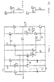
- an input terminal 10 is coupled to the base of a low impedance driver stage formed by emitter follower stage 11, comprising an NPN transistor having a collector connected to a supply line 12, and an emitter coupled via a current source 13 to a ground reference terminal 14.
- the emitter of the NPN transistor 11 is coupled to a PNP darlington stage 20 comprising PNP transistors 21 and 22.
- the emitters of the two PNP transistors 21 and 22 are coupled to the supply line 12, that of the transistor 21 being coupled to the supply line 12 via a resistor 23 which determines the current through the transistor 21 and also to the base of the transistor 22.
- the collector of the transistor 21 is coupled to the ground reference terminal 14.
- Input to the darlington stage 20 is coupled to the base of the transistor 21 whilst the output is taken from the collector of the transistor 22, which is coupled to drive the base of a current sourcing NPN transistor 30.
- the collector of the current sourcing transistor 30 is coupled to the supply line 12 whilst its emitter is coupled to an output terminal 80 to which in operation a load, such as a loudspeaker is connected.
- the transistors 21, 22 and 30 together with the resistor 23 form a current sourcing section for sourcing current to the output terminal 80.
- the emitter of the emitter follower transistor 11 is also coupled to the emitter of a cascode connected PNP transistor 50 whose base is coupled to a bias voltage source 40.
- the voltage source 40 comprises three PNP transistors 41, 42 and 43, one resistor 44 and one current source 45.
- the emitter of the PNP transistor 43 is coupled to the supply line 12.
- the PNP transistor 41 has its base coupled to the collector of the PNP transistor 43 and to the ground reference terminal 14 via a current source 45, has its collector coupled to the ground reference terminal 14 and its emitter coupled to the base and the collector of the PNP transistor 42.
- the emitter of the PNP transistor 42 is coupled to the base of the PNP transistor 43 and to the supply line 12 via the resistor 44 which fixes the current through the PNP transistors 41 and 42.
- the current source 45 supplies current to the PNP transistor 43.
- the output of the voltage source 40 is taken at the base of the PNP transistor 41 which is coupled to the base of the cascode transistor 50. It provides a voltage which is three base-emitter junction voltages from the supply line 12.
- the collector of the cascode transistor 50 is coupled to a current gain section including one resistor 62 and two NPN current mirror connected transistors 60 and 61, having a gain factor equal to the ratio of their emitter areas plus one.
- the emitters of the NPN transistors 60 and 61 are coupled together and to the ground reference terminal 14 via a resistor 62 which fixes the current through the transistors 50, 60 and 61.
- the bases of transistors 60 and 61 are connected together and to the collectors of the cascode PNP transistor 50 and the NpN transistor 61.
- the collector of npn transistor 60 is coupled to the supply line 12. If a high gain is required, the PNP transistor 61 is advantageously replaced by a resistor 63 coupled as shown in Figure 2a or 2b to form a NPN beta gain with resistor.
- the cascode PNP transistor 50 by virtue of the connections of its emitter to the base of the PNP darlington transistor 21 and of its base to the output of the voltage source 40, is operative to provide biasing voltage for that darlington stage. This means that the three base-emitter junction voltages of the voltage source 40 are matched with three base-emitter junctions of the PNP transistors 50,21 and 22. Once the collector current in the cascode PNP transistor 50 is supplied by the following current gain section, the current in the PNP transistor 22 is determined and is a function of the current source 45.
- the emitters of the current gain stage transistors 60 and 61 are coupled to drive a current sinking section 70 connected to sink current from the output terminal 80 during the appropriate half cycle of the input signal.
- the current sinking section comprises four NPN transistors 71, 72, 73 74 and two resistors 75 and 76.
- the emitters of the transistors 60 and 61 of the current gain section are coupled to the base of the NPN transistor 72 and to that of the NPN transistor 71 via a resistor 75.
- the emitters of the NPN transistors 71 and 72 are coupled to the ground reference terminal 14.
- the collector of the NPN transistor 71 is coupled in its turn to the collector of the PNP transistor 22 of the PNP darlington stage via the NPN transistor 74 connected as a diode, while the collector of the NPN transistor 72 is coupled to output terminal 80.
- the vital loop is created to ensure the good bias of the circuit.
- the current from the collector of the PNP transistor 22 fixes the current in the collector of the NPN transistor 71.
- the coupling between the bases of the transistors 71 and 72 fixes the current in the collector of the transistor 72 which in turn fixes the current in the transistor 30.
- the amplitude of the collector quiescent current of the transistor 72 depends on the ratio of the emitter areas of the transistors 71 and 72.
- the NPN transistor 73 mounted as a diode between the collectors of the transistors 71 and 72, is used to prevent saturation of the transistor 71 at a middle sinking current.
- the resistor 75 limits the collector current of the transistor 71 and allows the voltage at the output terminal 80 to reach the value of the saturation voltage of the transistor 72.
- the diode connected transistor 74 and the resistor 76 coupled between the collectors of the transistors 71 and 72 are used to smooth the cross-over passage.
- a Miller capacitance 81 coupled between the input terminal 10 and output terminal 80 is used to compensate the amplifier frequency phase shift.
- an oscillating input signal such as the audio signal from a preamplifier, is applied to the input terminal 10 of the amplifier.
- the emitter follower During the half cycle of the input signal in which current is fed into the base of the emitter follower stage transistor 11, the emitter follower provides an emitter dynamic output current which flows through the cascode transistor 50 into the current gain stage 60. This stage in turn drives the current section 70 which sinks current from the output terminal 80.
- the gain factor N can be chosen to obtain equality of the transfer function characteristic.
- the amplifier circuit of the invention has a number of advantages over the prior art circuits described previously. Although the circuit has a high current capability, it is inherently more stable than the prior art circuits due to its being driven by an emitter follower stage which provides a low impedance drive.
- Biasing of the circuit by way of the cascode stage 50 is extremely simple and stable.
Landscapes
- Engineering & Computer Science (AREA)
- Power Engineering (AREA)
- Amplifiers (AREA)
Applications Claiming Priority (2)
| Application Number | Priority Date | Filing Date | Title |
|---|---|---|---|
| GB8828917 | 1988-12-10 | ||
| GB8828917A GB2227137B (en) | 1988-12-10 | 1988-12-10 | Amplifier output stage |
Publications (3)
| Publication Number | Publication Date |
|---|---|
| EP0373853A2 true EP0373853A2 (fr) | 1990-06-20 |
| EP0373853A3 EP0373853A3 (fr) | 1991-01-09 |
| EP0373853B1 EP0373853B1 (fr) | 1997-04-09 |
Family
ID=10648327
Family Applications (1)
| Application Number | Title | Priority Date | Filing Date |
|---|---|---|---|
| EP89312899A Expired - Lifetime EP0373853B1 (fr) | 1988-12-10 | 1989-12-11 | Etage de sortie amplificateur |
Country Status (8)
| Country | Link |
|---|---|
| US (1) | US5021746A (fr) |
| EP (1) | EP0373853B1 (fr) |
| JP (1) | JP2816584B2 (fr) |
| KR (1) | KR930007291B1 (fr) |
| DE (1) | DE68927951T2 (fr) |
| GB (1) | GB2227137B (fr) |
| HK (1) | HK106995A (fr) |
| SG (1) | SG30646G (fr) |
Cited By (1)
| Publication number | Priority date | Publication date | Assignee | Title |
|---|---|---|---|---|
| EP1014567A3 (fr) * | 1998-12-18 | 2003-07-09 | Texas Instruments Incorporated | Perfectionnements apportés à un amplificateur opérationnel |
Families Citing this family (3)
| Publication number | Priority date | Publication date | Assignee | Title |
|---|---|---|---|---|
| US5500625A (en) * | 1994-12-01 | 1996-03-19 | Texas Instruments Incorporated | Controlled current output stage amplifier circuit and method |
| US5764105A (en) * | 1996-11-22 | 1998-06-09 | Burr-Brown Corporation | Push-pull output circuit method |
| US6417733B1 (en) * | 1999-07-06 | 2002-07-09 | Texas Instruments Incorporated | High output voltage swing class AB operational amplifier output stage |
Family Cites Families (15)
| Publication number | Priority date | Publication date | Assignee | Title |
|---|---|---|---|---|
| GB1274672A (en) * | 1968-09-27 | 1972-05-17 | Rca Corp | Operational amplifier |
| BE756600A (fr) * | 1969-09-26 | 1971-03-24 | Philips Nv | Amplificateur de courant |
| US3660773A (en) * | 1970-02-05 | 1972-05-02 | Motorola Inc | Integrated circuit amplifier having an improved gain-versus-frequency characteristic |
| CA965159A (en) * | 1970-06-30 | 1975-03-25 | Bendix Corporation (The) | Half-bridge audio amplifier |
| JPS567322B2 (fr) * | 1972-03-21 | 1981-02-17 | ||
| JPS5422859B2 (fr) * | 1972-12-30 | 1979-08-09 | ||
| US4025871A (en) * | 1974-01-22 | 1977-05-24 | General Electric Company | Audio amplifier for integrated circuit fabrication having controlled idling current |
| US3979689A (en) * | 1975-01-29 | 1976-09-07 | Rca Corporation | Differential amplifier circuit |
| JPS5272451U (fr) * | 1975-11-27 | 1977-05-30 | ||
| JPS52136526U (fr) * | 1976-04-09 | 1977-10-17 | ||
| JPS55143809A (en) * | 1979-04-25 | 1980-11-10 | Hitachi Ltd | Push-pull circuit |
| JP2636829B2 (ja) * | 1981-12-17 | 1997-07-30 | 富士通株式会社 | 差動回路 |
| JPS598415A (ja) * | 1982-07-06 | 1984-01-17 | Toshiba Corp | 増幅回路 |
| NL8204003A (nl) * | 1982-10-18 | 1984-05-16 | Philips Nv | Schakelversterker. |
| JPS60160707A (ja) * | 1984-01-31 | 1985-08-22 | Matsushita Electric Ind Co Ltd | プッシュプル型出力回路 |
-
1988
- 1988-12-10 SG SG1995907168A patent/SG30646G/en unknown
- 1988-12-10 GB GB8828917A patent/GB2227137B/en not_active Expired - Fee Related
-
1989
- 1989-12-06 JP JP1318715A patent/JP2816584B2/ja not_active Expired - Lifetime
- 1989-12-07 US US07/447,353 patent/US5021746A/en not_active Expired - Fee Related
- 1989-12-07 KR KR1019890018068A patent/KR930007291B1/ko not_active Expired - Fee Related
- 1989-12-11 EP EP89312899A patent/EP0373853B1/fr not_active Expired - Lifetime
- 1989-12-11 DE DE68927951T patent/DE68927951T2/de not_active Expired - Fee Related
-
1995
- 1995-06-29 HK HK106995A patent/HK106995A/xx not_active IP Right Cessation
Cited By (1)
| Publication number | Priority date | Publication date | Assignee | Title |
|---|---|---|---|---|
| EP1014567A3 (fr) * | 1998-12-18 | 2003-07-09 | Texas Instruments Incorporated | Perfectionnements apportés à un amplificateur opérationnel |
Also Published As
| Publication number | Publication date |
|---|---|
| SG30646G (en) | 1995-09-01 |
| JPH02237205A (ja) | 1990-09-19 |
| GB8828917D0 (en) | 1989-01-18 |
| HK106995A (en) | 1995-07-07 |
| KR900011130A (ko) | 1990-07-11 |
| DE68927951D1 (de) | 1997-05-15 |
| KR930007291B1 (ko) | 1993-08-04 |
| GB2227137A (en) | 1990-07-18 |
| DE68927951T2 (de) | 1997-10-16 |
| JP2816584B2 (ja) | 1998-10-27 |
| EP0373853A3 (fr) | 1991-01-09 |
| GB2227137B (en) | 1993-02-10 |
| EP0373853B1 (fr) | 1997-04-09 |
| US5021746A (en) | 1991-06-04 |
Similar Documents
| Publication | Publication Date | Title |
|---|---|---|
| US5786731A (en) | Class AB complementary transistor output stage having large output swing and large output drive | |
| US6542030B2 (en) | Amplifier with stabilization means | |
| GB2084420A (en) | Output amplifier | |
| US4827223A (en) | Buffer amplifier | |
| US4723111A (en) | Amplifier arrangement | |
| JPH0612859B2 (ja) | 差動増幅器回路 | |
| US4254379A (en) | Push-pull amplifier circuit | |
| US4922208A (en) | Output stage for an operational amplifier | |
| US4274060A (en) | Signal change-over amplifier | |
| US4587491A (en) | IC class AB amplifier output stage | |
| EP0196703A1 (fr) | Montage amplificateur | |
| EP0209334B1 (fr) | Circuit miroir de courant | |
| US4587494A (en) | Quasi-complementary class B IC output stage | |
| JP2001203544A (ja) | 増幅器装置及び増幅方法 | |
| US5021746A (en) | Amplifier output stage | |
| US4607233A (en) | Push-pull amplifier circuit with stable class AB operation | |
| US5144259A (en) | Amplifier having a push-pull out-put stage | |
| KR930007294B1 (ko) | 달링턴 트랜지스터 장치 | |
| US4453134A (en) | High voltage operational amplifier | |
| JPH0580162B2 (fr) | ||
| US4491804A (en) | Bias circuit which is independent of output device voltage characteristics for biasing an amplifier in class AB operation | |
| EP1352473A1 (fr) | Phase d'entree avec impedance d'entree selectionnable | |
| US20020101268A1 (en) | Operational amplifier output stage | |
| JPS6040729B2 (ja) | 電力増幅器 | |
| EP0120125A1 (fr) | Circuit de polarisation d'un amplificateur de classe AB qui ne dépend pas des caractéristiques de tension du stade final |
Legal Events
| Date | Code | Title | Description |
|---|---|---|---|
| PUAI | Public reference made under article 153(3) epc to a published international application that has entered the european phase |
Free format text: ORIGINAL CODE: 0009012 |
|
| AK | Designated contracting states |
Kind code of ref document: A2 Designated state(s): DE ES FR IT NL SE |
|
| PUAL | Search report despatched |
Free format text: ORIGINAL CODE: 0009013 |
|
| AK | Designated contracting states |
Kind code of ref document: A3 Designated state(s): DE ES FR IT NL SE |
|
| 17P | Request for examination filed |
Effective date: 19910708 |
|
| 17Q | First examination report despatched |
Effective date: 19931004 |
|
| GRAG | Despatch of communication of intention to grant |
Free format text: ORIGINAL CODE: EPIDOS AGRA |
|
| GRAH | Despatch of communication of intention to grant a patent |
Free format text: ORIGINAL CODE: EPIDOS IGRA |
|
| GRAH | Despatch of communication of intention to grant a patent |
Free format text: ORIGINAL CODE: EPIDOS IGRA |
|
| ITF | It: translation for a ep patent filed | ||
| GRAA | (expected) grant |
Free format text: ORIGINAL CODE: 0009210 |
|
| AK | Designated contracting states |
Kind code of ref document: B1 Designated state(s): DE ES FR IT NL SE |
|
| PG25 | Lapsed in a contracting state [announced via postgrant information from national office to epo] |
Ref country code: NL Effective date: 19970409 Ref country code: ES Free format text: THE PATENT HAS BEEN ANNULLED BY A DECISION OF A NATIONAL AUTHORITY Effective date: 19970409 |
|
| REF | Corresponds to: |
Ref document number: 68927951 Country of ref document: DE Date of ref document: 19970515 |
|
| PG25 | Lapsed in a contracting state [announced via postgrant information from national office to epo] |
Ref country code: SE Effective date: 19970709 |
|
| ET | Fr: translation filed | ||
| NLV1 | Nl: lapsed or annulled due to failure to fulfill the requirements of art. 29p and 29m of the patents act | ||
| PLBE | No opposition filed within time limit |
Free format text: ORIGINAL CODE: 0009261 |
|
| STAA | Information on the status of an ep patent application or granted ep patent |
Free format text: STATUS: NO OPPOSITION FILED WITHIN TIME LIMIT |
|
| 26N | No opposition filed | ||
| PGFP | Annual fee paid to national office [announced via postgrant information from national office to epo] |
Ref country code: DE Payment date: 20001014 Year of fee payment: 12 |
|
| PGFP | Annual fee paid to national office [announced via postgrant information from national office to epo] |
Ref country code: FR Payment date: 20001204 Year of fee payment: 12 |
|
| PG25 | Lapsed in a contracting state [announced via postgrant information from national office to epo] |
Ref country code: DE Free format text: LAPSE BECAUSE OF NON-PAYMENT OF DUE FEES Effective date: 20020702 |
|
| PG25 | Lapsed in a contracting state [announced via postgrant information from national office to epo] |
Ref country code: FR Free format text: LAPSE BECAUSE OF NON-PAYMENT OF DUE FEES Effective date: 20020830 |
|
| REG | Reference to a national code |
Ref country code: FR Ref legal event code: ST |
|
| REG | Reference to a national code |
Ref country code: FR Ref legal event code: D6 |
|
| PG25 | Lapsed in a contracting state [announced via postgrant information from national office to epo] |
Ref country code: IT Free format text: LAPSE BECAUSE OF NON-PAYMENT OF DUE FEES Effective date: 20051211 |