EP0373887A2 - Fernsprechweckdetektor - Google Patents
Fernsprechweckdetektor Download PDFInfo
- Publication number
- EP0373887A2 EP0373887A2 EP89312973A EP89312973A EP0373887A2 EP 0373887 A2 EP0373887 A2 EP 0373887A2 EP 89312973 A EP89312973 A EP 89312973A EP 89312973 A EP89312973 A EP 89312973A EP 0373887 A2 EP0373887 A2 EP 0373887A2
- Authority
- EP
- European Patent Office
- Prior art keywords
- ringing
- signal
- detector
- predetermined
- integral
- Prior art date
- Legal status (The legal status is an assumption and is not a legal conclusion. Google has not performed a legal analysis and makes no representation as to the accuracy of the status listed.)
- Granted
Links
Images


Classifications
-
- G—PHYSICS
- G01—MEASURING; TESTING
- G01R—MEASURING ELECTRIC VARIABLES; MEASURING MAGNETIC VARIABLES
- G01R15/00—Details of measuring arrangements of the types provided for in groups G01R17/00 - G01R29/00, G01R33/00 - G01R33/26 or G01R35/00
-
- H—ELECTRICITY
- H04—ELECTRIC COMMUNICATION TECHNIQUE
- H04M—TELEPHONIC COMMUNICATION
- H04M19/00—Current supply arrangements for telephone systems
- H04M19/02—Current supply arrangements for telephone systems providing ringing current or supervisory tones, e.g. dialling tone or busy tone
- H04M19/04—Current supply arrangements for telephone systems providing ringing current or supervisory tones, e.g. dialling tone or busy tone the ringing-current being generated at the substations
Definitions
- This invention is in the field of telephone line equipment, and more particularly, telephone line equipment that can detect valid ringing signals and pass them on to other equipment.
- the telephone art In the telephone art, several different electrical signals are transmitted over the pair of wires that connects each telephone instrument to the central office.
- the audio voice signal there is the off-hook signal which indicates that the telephone instrument is in use, the dialing signal which transmits the telephone number dialed, and the ringing signal which causes an alerting device to operate. Since the original alerting devices were bells, that signal is known as a ringing signal.
- the ringing signal is a high voltage alternating current signal with a frequency of approximately 20Hz.
- Various circuits have been devised which reliably distinguish valid ringing signals from among the other signals and the many types of noise that can exist on a telephone line.
- This distinctive ringing has been available within the confines of a private branch exchange (PBX) which serves a single location. Because the pre-existing ringing detectors could not reliably detect these distinctive ringing signals, a new detector was devised which operated very well within the confines of a PBX system.
- U.S. Patent 4,491,691 which issued to Embree et al. on January 1, 1985 describes such a ringing detecting system.
- a digital magnitude comparator produces a binary output indicative of whether the tip-ring voltage, that is, the telephone line voltage, exceeds a predetermined magnitude.
- the integrator generates a time integral of the digital output; when the time integral exceeds a predetermined value, ringing is indicated.
- Our invention provides much more accurate detection of ringing signals in the off-premise environment and eliminates the need for a low impedance power dissipating bridge.
- a magnitude comparator coupled to the input signal produces a binary signal indicative of whether the instantaneous magnitude of the input signal exceeds a predetermined magnitude.
- An integrator produces a time integral of the binary signal, and a timer controls the interval of time over which the binary signal is integrated.
- Integral comparison means responsive to the integrator indicates the presence of a valid ringing signal if, at the end of the integrating interval the integral exceeds a predetermined integral value. The proper setting of the integrating interval can greatly enhance the accuracy of the detector.
- the timer may also control the minimum lengths of time that the presence and absence of a valid ringing signal are indicated for distinctive ringing applications.
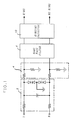
- FIG 1 shows a typical application of the ringing detector of the invention.
- a telephone line circuit has two conductors T and R, commonly designated as tip and ring, respectively.
- a lightning protection circuit 2 and a high impedance attenuator 4 may be connected across the tip and ring terminals to provide a protected analog output signal of suitable voltage with minimum disturbance of the telephone line circuit.
- a band pass filter 6 may have its input connected to the output of attenuator 4 and its output connected to the input of a ringing detector 10.
- the band pass characteristic of filter 6 is not critical; its main purpose is to block dc and interference from power frequencies (50Hz Bnd 60Hz) and to pass frequencies in the broad vicinity of ringing signals.
- Ringing detector 10 may have one or more binary outputs for indicating ringing and no ringing.
- a magnitude comparator 12 receives its analog input signal ⁇ TR indirectly from the telephone line circuit.
- Its output signal PK is a binary signal which may, for example, be high only when the input voltage magnitude is above a convenient predetermined level. That level may correspond to approximately 20V RMS across the tip-ring pair.
- integrator 18 is a digital -1 to 31 up/down counter that samples the input at a 1KHz rate, counts up if the input is high, and counts down if it is low. Integrator 18 holds its count at either limit without resetting. Combinational logic within integrator 18 provides outputs that indicate when the count, therefore the time integral, is at -1, less than 5, less than 8, and less than 16, respectively. A "SET TO ZERO" input momentarily resets the count to zero when it goes high.
- the invention is not limited to the digital integrator shown; other integrators, both analog and digital can be used to generate a time integral of the PK binary signal.
- NO-ring flip flop 17 has a " Q " output connected to the "SET TO ZERO” input of integrator 18.
- the " Q " output of flip flop 17 goes high when its "RESET” input goes high, and goes low when its "SET” input goes high.
- Negative transition detector 14 puts out a pulse on its "TRANS” output when its input goes high to low.
- a zero-to-99 millisecond timer 20 has a "CLEAR” input, a “DISABLE” input, a "72" output and a “99" output
- timer 20 begins counting in milliseconds from zero. Its outputs go high for their respective millisecond count.
- the "DISABLE” input is high, the timer stops wherever it happens to be.
- a 72-to-99-count latch 22 has inputs connected to the "72" and “99" outputs respectively of timer 20, and a "HOLD" output.
- the "HOLD" output of latch 22 is high whenever the time count is above 72 milliseconds and below 99 milliseconds.
- An AND gate 24 has an inverting input connected to the " ⁇ 5" output of integrator 18 and non-inverting inputs connected to the "72" output of timer 20 and the " ⁇ 16” output of integrator 18, respectively.
- the output of AND gate 24 is connected to the "DISABLE” input of timer 20.
- An AND gate 26 has an input connected to the "72" output of timer 20, an inverting input connected to the " ⁇ 16" output of integrator 18, and an output "RNGP".
- a no-ringing logic circuit 28 has a "NRNG” input, a “72” input connected to the “72” output of timer 20, " ⁇ 5" and “-1” inputs, connected to the " ⁇ 5" and “-1 ⁇ outputs respectively, of integrator 18 and a “NRNGP” output.
- the "NRNGP” output puts out a pulse whenever inputs "72" and “ ⁇ 5" are both high or inputs "NRNG” and "-1 ⁇ are both high.
- a ringing detector output latch 31 has a “SET” input connected to the “NRNGP” output of logic circuit 28, a “RESET” input connected to the "RNGP” output of AND gate 26, and a “Q” output, which goes high when the "SET” input goes high.
- the "Q” output provides the "NRNG” output signal of this ringing detector embodiment of the invention, and is connected to the "NRNG” input of no-ringing logic circuit 28.
- a flip flop 34 has a “SET” input connected to the “ ⁇ 8” output of integrator 18, a “RESET” input connected to the output of AND gate 26, and a "Q" output.
- a timer control logic circuit 36 has a "CLEAR” output connected to the "CLEAR” input of timer 20 and four inputs.
- a “TRANS” input is connected to the output of negative transition detecting latch 14, a “NLOAD” input is connected to the " Q " output of flip flop 17, an "INH” input is connected to the "Q” output of flip flop 34, and a “HOLD” input is connected to the "HOLD" output of latch 22.
- the "CLEAR" output of logic circuit 36 goes high whenever the "HOLD" input is low in combination with either the "NLOAD” input being low or both the "INH” and "TRANS” inputs being low.
- FIG 3 is a timing diagram that shows signals that may exist simultaneously at various locations throughout the circuit. Each signal is labeled according to its physical location in the diagram of FIG 2.
- the signal on the first line of FIG 3 is the attenuated and filtered version of the differential tip-ring voltage of the telephone line circuit, and the only analog signal in this diagram.
- Dotted lines 36 and 38 represent the voltage levels that correspond to the switching levels of magnitude comparator 12.
- PK goes high; flip-flop 17 is reset, driving NLOAD high and resetting integrator 18 to zero; and integrator 18 starts counting up at a rate of one count per millisecond.
- HOLD being low, when NLOAD goes high, the "CLEAR" output of timer control logic 36 goes low, and millisecond timer 20 starts at zero.
- Integrator 18 counts up when PK is high and down when PK is low. Signals ⁇ 5, ⁇ 8 and ⁇ 16 go low after 5,8 and 16 mllliseconds, respectively.
- ⁇ TR drops below level 36
- PK goes low and integrator 18 begins to count down.
- negative transition detector 14 momentarily goes low.
- the ⁇ 16 signal may go high for a short interval as the count of integrator 18 dips back below 16 during a "countdown" period. Since ⁇ TR soon drops below level 38, however, the PK signal from magnitude comparator 12 again goes high, and integrator 18 soon counts above 16 again to its maximum count, 31. The count remains near 31 as long as the strong ac signal continues across the TIP-RING pair, lowering periodically during the short count-down intervals and rising right back to 31 during the longer count-up intervals.
- HOLD signal remains high, timer 20 continues to count. At 99 msec, the HOLD signal goes low, and timer 20 recycles through zero. About 8 milliseconds later, the TRANS signal from transition detector 14 momentarily goes low in response to the PK transition from high to low. Since both HOLD and INH are also low, CLEAR goes high, and timer 20 restarts at zero. This continues to happen each time TRANS goes low until the ringing signal disappears and the integral count drops below 8, causing INH to go high again. In this manner, the end of each ringing pulse is accurately timed. The NRNG output signal, however, does not change at this point.
- the minimum time for either a RINGING or NO RINGING output indication is the full cycle time of counter 20, 100 msec. This is a requirement for a known distinctive ringing application. This minimum time can readily be changed by simply changing the full cycle time of timer 20, and output "99" to match. Similarly, if different minimum RINGING and NO RINGING indication times are desired, different timer counts should enable gate 26 and logic 28, respectively.
- FIG 2 can be readily assembled by persons skilled in the art from available components.
- Latches 22 and 31, negative transition detector 14, and logic circuits 38 and 36 can be made from a combination of simple logic gates.
- Timer 20 and integrator 18 each might include a source of 1 msec clock pulses, a counter, and decoding logic to provide the necessary output values.
- the 1 msec clock can, of course, be shared.
- Flip-flops 17 and 34 can be of the variety in which the data is clocked in (using a higher frequency clock such as 128 KHz, eg.) to prevent race conditions.
- magnitude comparator 12 can be implemented by a full wave rectifier, a differential amplifier and a reference voltage source.
Landscapes
- Engineering & Computer Science (AREA)
- Signal Processing (AREA)
- Physics & Mathematics (AREA)
- General Physics & Mathematics (AREA)
- Measurement Of Current Or Voltage (AREA)
- Telephonic Communication Services (AREA)
- Devices For Supply Of Signal Current (AREA)
- Telephone Function (AREA)
Applications Claiming Priority (2)
| Application Number | Priority Date | Filing Date | Title |
|---|---|---|---|
| US283776 | 1988-12-13 | ||
| US07/283,776 US4939775A (en) | 1988-12-13 | 1988-12-13 | Telephone ringing detector |
Publications (3)
| Publication Number | Publication Date |
|---|---|
| EP0373887A2 true EP0373887A2 (de) | 1990-06-20 |
| EP0373887A3 EP0373887A3 (de) | 1991-10-23 |
| EP0373887B1 EP0373887B1 (de) | 1995-08-02 |
Family
ID=23087501
Family Applications (1)
| Application Number | Title | Priority Date | Filing Date |
|---|---|---|---|
| EP89312973A Expired - Lifetime EP0373887B1 (de) | 1988-12-13 | 1989-12-12 | Fernsprechweckdetektor |
Country Status (6)
| Country | Link |
|---|---|
| US (1) | US4939775A (de) |
| EP (1) | EP0373887B1 (de) |
| JP (1) | JPH0785565B2 (de) |
| KR (1) | KR0138267B1 (de) |
| CA (1) | CA2005260C (de) |
| DE (1) | DE68923689T2 (de) |
Cited By (1)
| Publication number | Priority date | Publication date | Assignee | Title |
|---|---|---|---|---|
| US5880850A (en) * | 1996-04-18 | 1999-03-09 | American Air Liquide Inc | Method and system for sensitive detection of molecular species in a vacuum by harmonic detection spectroscopy |
Families Citing this family (8)
| Publication number | Priority date | Publication date | Assignee | Title |
|---|---|---|---|---|
| JPH0817437B2 (ja) * | 1989-11-29 | 1996-02-21 | シャープ株式会社 | ファクシミリ装置 |
| US5228081A (en) * | 1990-10-18 | 1993-07-13 | Ag Communication Systems Corporation | Ringing signal control circuit for an enhanced subscriber line interface |
| US5361296A (en) * | 1991-11-25 | 1994-11-01 | Zoom Telephonics, Inc. | Modem with ring detection/modem processing capability |
| US5544241A (en) * | 1995-06-27 | 1996-08-06 | Andrew S. Dibner | Telephone ring detector |
| US6058171A (en) * | 1996-08-14 | 2000-05-02 | Oakley Telecom, Lc | Unique ring caller ID |
| JPH10308801A (ja) | 1997-05-09 | 1998-11-17 | Matsushita Electric Ind Co Ltd | 電話機 |
| US5920624A (en) * | 1997-06-16 | 1999-07-06 | Dasym Technologies Inc. | Telephone ring signal detector |
| US7110798B2 (en) * | 2002-05-09 | 2006-09-19 | Shary Nassimi | Wireless headset |
Family Cites Families (9)
| Publication number | Priority date | Publication date | Assignee | Title |
|---|---|---|---|---|
| US3603740A (en) * | 1969-08-18 | 1971-09-07 | Northern Electric Co | Method and means for ringing a telephone subset |
| US3808379A (en) * | 1972-05-30 | 1974-04-30 | Gte Automatic Electric Lab Inc | Telephone tone ringer |
| US3816669A (en) * | 1972-11-01 | 1974-06-11 | Electrospace Corp | Apparatus for detecting telephone ringing signals |
| JPS52132609A (en) * | 1976-04-30 | 1977-11-07 | Pioneer Electronic Corp | Starting circuit |
| US4066848A (en) * | 1976-09-07 | 1978-01-03 | T.A.D. | Telephone ring detector circuit |
| US4390843A (en) * | 1981-02-09 | 1983-06-28 | Paradyne Corporation | Telephone system ring period detector |
| FR2532133A1 (fr) * | 1982-08-17 | 1984-02-24 | Labo Cent Telecommunicat | Circuit de sonnerie pour poste telephonique, realisable en circuit integre |
| US4491691A (en) * | 1983-02-28 | 1985-01-01 | At&T Bell Laboratories | Electronic tone ringer |
| JPS61237559A (ja) * | 1985-04-15 | 1986-10-22 | Ricoh Co Ltd | 呼出信号検出回路 |
-
1988
- 1988-12-13 US US07/283,776 patent/US4939775A/en not_active Expired - Lifetime
-
1989
- 1989-12-12 CA CA002005260A patent/CA2005260C/en not_active Expired - Fee Related
- 1989-12-12 DE DE68923689T patent/DE68923689T2/de not_active Expired - Fee Related
- 1989-12-12 EP EP89312973A patent/EP0373887B1/de not_active Expired - Lifetime
- 1989-12-13 JP JP1321595A patent/JPH0785565B2/ja not_active Expired - Lifetime
- 1989-12-13 KR KR1019890018442A patent/KR0138267B1/ko not_active Expired - Fee Related
Cited By (1)
| Publication number | Priority date | Publication date | Assignee | Title |
|---|---|---|---|---|
| US5880850A (en) * | 1996-04-18 | 1999-03-09 | American Air Liquide Inc | Method and system for sensitive detection of molecular species in a vacuum by harmonic detection spectroscopy |
Also Published As
| Publication number | Publication date |
|---|---|
| KR900010403A (ko) | 1990-07-07 |
| JPH0785565B2 (ja) | 1995-09-13 |
| KR0138267B1 (ko) | 1998-06-15 |
| DE68923689D1 (de) | 1995-09-07 |
| EP0373887B1 (de) | 1995-08-02 |
| EP0373887A3 (de) | 1991-10-23 |
| DE68923689T2 (de) | 1996-01-25 |
| JPH02244944A (ja) | 1990-09-28 |
| CA2005260A1 (en) | 1990-06-13 |
| CA2005260C (en) | 1994-03-08 |
| US4939775A (en) | 1990-07-03 |
Similar Documents
| Publication | Publication Date | Title |
|---|---|---|
| JPH06105948B2 (ja) | 呼出信号検出装置 | |
| CA1270585A (en) | Rotary dial pulse receiver | |
| EP0373887B1 (de) | Fernsprechweckdetektor | |
| US5218635A (en) | Low-frequency alternating current signal detector, in particular for central office line interface circuits | |
| EP0089687B1 (de) | Verfahren und elektronische Vorrichtung zum Erkennen des Abhebens des Telefonhörers bei Vorhandensein von Rufstrom | |
| US4455456A (en) | Digital supervisory circuit for a telephone system | |
| EP0116291B1 (de) | Rufabschaltungserkennungssystem | |
| US4536619A (en) | Ringing signal detection circuit | |
| US4092489A (en) | Switching arrangement for monitoring polarity reversal on lines in telecommunication systems | |
| US5392347A (en) | Ringing tone signal detecting circuit | |
| CA2016258C (en) | Telephone line interface circuit | |
| CA1067635A (en) | Telephone metering interface with reverse signal sensor | |
| USRE29078E (en) | Key telephone system | |
| GB2032730A (en) | Signal processing apparatus for subscriber circuits | |
| US4028501A (en) | Method and apparatus for translating multiple frequency signalling | |
| EP0255374A2 (de) | Fernsprechschaltung zum Zuführen von Wecksignalen an eine Fernsprechteilnehmerleitung und für die Erkennung des Abhebens während des Weckens | |
| KR900000722B1 (ko) | 호출신호 전송장치 | |
| US3993875A (en) | Tone receiver | |
| CA1138581A (en) | Loop, dial pulse and ring trip detection circuit with capacitive shunt network | |
| CA1259146A (en) | Dial tone detector | |
| JPH0243884A (ja) | 着信検出回路 | |
| US6944286B1 (en) | Ground key detection circuit and method for interference-resistant detection of the activation of a ground key for telephones | |
| JPS60169263A (ja) | 遠隔制御方式 | |
| CA1211240A (en) | Ring trip detection system | |
| SU1022331A1 (ru) | Устройство контрол состо ни абонентского шлейфа |
Legal Events
| Date | Code | Title | Description |
|---|---|---|---|
| PUAI | Public reference made under article 153(3) epc to a published international application that has entered the european phase |
Free format text: ORIGINAL CODE: 0009012 |
|
| AK | Designated contracting states |
Kind code of ref document: A2 Designated state(s): DE FR GB NL SE |
|
| PUAL | Search report despatched |
Free format text: ORIGINAL CODE: 0009013 |
|
| AK | Designated contracting states |
Kind code of ref document: A3 Designated state(s): DE FR GB NL SE |
|
| 17P | Request for examination filed |
Effective date: 19920415 |
|
| 17Q | First examination report despatched |
Effective date: 19940304 |
|
| RAP3 | Party data changed (applicant data changed or rights of an application transferred) |
Owner name: AT&T CORP. |
|
| GRAA | (expected) grant |
Free format text: ORIGINAL CODE: 0009210 |
|
| AK | Designated contracting states |
Kind code of ref document: B1 Designated state(s): DE FR GB NL SE |
|
| ET | Fr: translation filed | ||
| REF | Corresponds to: |
Ref document number: 68923689 Country of ref document: DE Date of ref document: 19950907 |
|
| PLBE | No opposition filed within time limit |
Free format text: ORIGINAL CODE: 0009261 |
|
| STAA | Information on the status of an ep patent application or granted ep patent |
Free format text: STATUS: NO OPPOSITION FILED WITHIN TIME LIMIT |
|
| 26N | No opposition filed | ||
| PGFP | Annual fee paid to national office [announced via postgrant information from national office to epo] |
Ref country code: SE Payment date: 20000928 Year of fee payment: 12 |
|
| PGFP | Annual fee paid to national office [announced via postgrant information from national office to epo] |
Ref country code: NL Payment date: 20001130 Year of fee payment: 12 |
|
| PGFP | Annual fee paid to national office [announced via postgrant information from national office to epo] |
Ref country code: FR Payment date: 20011121 Year of fee payment: 13 |
|
| PGFP | Annual fee paid to national office [announced via postgrant information from national office to epo] |
Ref country code: GB Payment date: 20011126 Year of fee payment: 13 |
|
| PG25 | Lapsed in a contracting state [announced via postgrant information from national office to epo] |
Ref country code: SE Free format text: LAPSE BECAUSE OF NON-PAYMENT OF DUE FEES Effective date: 20011213 |
|
| PGFP | Annual fee paid to national office [announced via postgrant information from national office to epo] |
Ref country code: DE Payment date: 20011230 Year of fee payment: 13 |
|
| REG | Reference to a national code |
Ref country code: GB Ref legal event code: IF02 |
|
| PG25 | Lapsed in a contracting state [announced via postgrant information from national office to epo] |
Ref country code: NL Free format text: LAPSE BECAUSE OF NON-PAYMENT OF DUE FEES Effective date: 20020701 |
|
| EUG | Se: european patent has lapsed |
Ref document number: 89312973.4 |
|
| NLV4 | Nl: lapsed or anulled due to non-payment of the annual fee |
Effective date: 20020701 |
|
| PG25 | Lapsed in a contracting state [announced via postgrant information from national office to epo] |
Ref country code: GB Free format text: LAPSE BECAUSE OF NON-PAYMENT OF DUE FEES Effective date: 20021212 |
|
| PG25 | Lapsed in a contracting state [announced via postgrant information from national office to epo] |
Ref country code: DE Free format text: LAPSE BECAUSE OF NON-PAYMENT OF DUE FEES Effective date: 20030701 |
|
| GBPC | Gb: european patent ceased through non-payment of renewal fee | ||
| PG25 | Lapsed in a contracting state [announced via postgrant information from national office to epo] |
Ref country code: FR Free format text: LAPSE BECAUSE OF NON-PAYMENT OF DUE FEES Effective date: 20030901 |
|
| REG | Reference to a national code |
Ref country code: FR Ref legal event code: ST |