EP0375585B1 - Procédé pour fabriquer un dispositif du type BICMOS - Google Patents
Procédé pour fabriquer un dispositif du type BICMOS Download PDFInfo
- Publication number
- EP0375585B1 EP0375585B1 EP89480174A EP89480174A EP0375585B1 EP 0375585 B1 EP0375585 B1 EP 0375585B1 EP 89480174 A EP89480174 A EP 89480174A EP 89480174 A EP89480174 A EP 89480174A EP 0375585 B1 EP0375585 B1 EP 0375585B1
- Authority
- EP
- European Patent Office
- Prior art keywords
- layer
- oxide
- polysilicon
- process according
- emitter
- Prior art date
- Legal status (The legal status is an assumption and is not a legal conclusion. Google has not performed a legal analysis and makes no representation as to the accuracy of the status listed.)
- Expired - Lifetime
Links
Images


Classifications
-
- H—ELECTRICITY
- H10—SEMICONDUCTOR DEVICES; ELECTRIC SOLID-STATE DEVICES NOT OTHERWISE PROVIDED FOR
- H10D—INORGANIC ELECTRIC SEMICONDUCTOR DEVICES
- H10D84/00—Integrated devices formed in or on semiconductor substrates that comprise only semiconducting layers, e.g. on Si wafers or on GaAs-on-Si wafers
- H10D84/01—Manufacture or treatment
- H10D84/0107—Integrating at least one component covered by H10D12/00 or H10D30/00 with at least one component covered by H10D8/00, H10D10/00 or H10D18/00, e.g. integrating IGFETs with BJTs
- H10D84/0109—Integrating at least one component covered by H10D12/00 or H10D30/00 with at least one component covered by H10D8/00, H10D10/00 or H10D18/00, e.g. integrating IGFETs with BJTs the at least one component covered by H10D12/00 or H10D30/00 being a MOS device
-
- H—ELECTRICITY
- H10—SEMICONDUCTOR DEVICES; ELECTRIC SOLID-STATE DEVICES NOT OTHERWISE PROVIDED FOR
- H10D—INORGANIC ELECTRIC SEMICONDUCTOR DEVICES
- H10D84/00—Integrated devices formed in or on semiconductor substrates that comprise only semiconducting layers, e.g. on Si wafers or on GaAs-on-Si wafers
- H10D84/01—Manufacture or treatment
- H10D84/02—Manufacture or treatment characterised by using material-based technologies
- H10D84/03—Manufacture or treatment characterised by using material-based technologies using Group IV technology, e.g. silicon technology or silicon-carbide [SiC] technology
- H10D84/038—Manufacture or treatment characterised by using material-based technologies using Group IV technology, e.g. silicon technology or silicon-carbide [SiC] technology using silicon technology, e.g. SiGe
-
- H—ELECTRICITY
- H10—SEMICONDUCTOR DEVICES; ELECTRIC SOLID-STATE DEVICES NOT OTHERWISE PROVIDED FOR
- H10D—INORGANIC ELECTRIC SEMICONDUCTOR DEVICES
- H10D84/00—Integrated devices formed in or on semiconductor substrates that comprise only semiconducting layers, e.g. on Si wafers or on GaAs-on-Si wafers
- H10D84/40—Integrated devices formed in or on semiconductor substrates that comprise only semiconducting layers, e.g. on Si wafers or on GaAs-on-Si wafers characterised by the integration of at least one component covered by groups H10D12/00 or H10D30/00 with at least one component covered by groups H10D10/00 or H10D18/00, e.g. integration of IGFETs with BJTs
- H10D84/401—Combinations of FETs or IGBTs with BJTs
- H10D84/403—Combinations of FETs or IGBTs with BJTs and with one or more of diodes, resistors or capacitors
Definitions
- This invention relates to a method for manufacturing a Bi-CMOS semiconductor device and more particularly to a fabrication technique for producing a BI-CMOS device with vertical bipolar NPN and PNP components.
- Bi-CMOS technology (bipolar and CMOS transistors on a single semiconductor substrate) has become an increasingly attractive device technology because it can provide high performance (better than CMOS alone) without high power consumption (much lower than bipolar alone).
- One of the recognized drawbacks in fabricating such Bi-CMOS devices is the increased processing required to produce such high performance CMOS and bipolar components on the same chip.
- the skill in the art has been to combine the separate processing steps as known for each technology into a combined processing sequence. This has resulted in overly complicated processing plans, which plans are undesirable as they contain excessive processing steps and are time-consuming and costly. Therefore, there has been an ever increasing need for a Bi-CMOS device which can be fabricated with a greater integration of the bipolar and CMOS process steps.
- the invention herein incorporates a structure which was specially developed to be compatible with the bipolar and the CMOS device. With this structure, processing steps can now be shared to simplify the Bi-CMOS fabrication.
- U.S.-A No. 4.484.388 discloses a method for forming a Bi-CMOS structure whereas a different Bi-CMOS device is produced by an unrelated process which includes steps to form an emitter self-aligned to the base and form the gate oxide over the emitter.
- a bipolar-CMOS IC device is formed in a p- substrate with an n-layer by: forming n+ buried region for a bipolar transistor and n+ buried region in both substrate and n-layer; forming p+ buried region around n+ region and p+ buried region outside region; forming p+ isolation region extending from the surface of n-layer to buried region; forming vertical npn transistor in layer surrounded by isolation region; forming p-well from the surface of n-layer to buried region; forming n-MOSFET in p-well; and, forming p-MOSFET in portion of n-layer on buried region.
- complementary bipolar-CMOS device is formed on a single substrate with complete prevention oif latch up.
- a method for fabricating a BI-CMOS device using fewer processing steps combined with the incorporation of a vertical PNP and NPN bipolar device is disclosed in claim 1.
- a bipolar structure for the device is configured which is closer to and more compatible with that of the FET.
- some of the generalized processing steps include: forming the reach-through N+ subcollector to the bipolar device without extra processing steps; combining into one mask the threshold adjust/well implants with self-aligned isolation leakage protection implants by using a self-aligned, removable oxide mask prior to field isolation; using a resist etch-back scheme to protect against emitter to base punch-through while self-aligning the pedestal and base; and also providing for the removal of the gate oxide at the emitter while maintaining it at the FET, without extra masks.
- the combination of the bipolar devices with the CMOS device can now be expanded.
- a vertical PNP can now be added to the device in addition to the CMOS component and vertical NPN. This permits additional flexibility in circuit design, as for example, where the vertical PNP's subcollector is tied to the substrate to create a particular circuit.
- the device structure is such that the bipolar and CMOS components can share similar structural features.
- the NPN and pFET share the same well and share a diffusion (the p+ extrinsic base is the same as the p+ source).
- the pnp and nFET share the same well and an n+ diffusion. This permits the merging of components which results in reduced component count and increased density.
- the circuit design is an emitter follower circuit, the subcollectors are tied to a constant voltage, which means that the collector capacitance is not critical since there is no charging and discharging.
- trench isolation (often used to reduce collector area by cutting it off and, therefore, collector capacitance) is not necessary. This makes the processing sequence simpler as recessed oxide isolation can be used.
- LDD lightly doped drain
- the vertical PNP is incorporated into the Bi-CMOS device without limitation to a particular circuit.
- trench isolation will be used to provide lateral isolation.
- the isolation to the substrate can then be accomplished either by using an oxygen implant to form a buried insulation layer or by starting with an n- (on p+) epi and ensuring that the p+ subcollector does not extend through the n- epi and touch the p+ substrate.
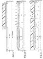
- Figures 1-11 are cross-sectional views in the fabrication sequence of the subject Bi-CMOS device.
- a P- epi layer 3 onto a P+ substrate 1 is deposited a P- epi layer 3.
- the starting wafer is a P- epi on a P+ substrate except if the PNP is to be isolated by N- epi on P+ substrate.
- the epi layer thickness is chosen so that, at the process end, the n+ subcollector junction depth is about 1 ⁇ m more shallow than the P-/P+ transition to avoid high capacitance/low voltage breakdown. This yields an epi layer thickness on the order of 3-6 ⁇ m.
- the subcollector areas 15 and 17 are driven-in and oxidized to thicknesses 19 and 21 of approximately 2000 Angström - 5000 Angström to lower the resistance and remove any implant or RIE damage.
- the areas covered by nitride mask 7 will not be oxidized and the resulting difference in height will provide a feature by which to align subsequent masks.
- the nitride layer 7 is now stripped using, for example, H3PO4.
- a boron implant (1013-1014cm ⁇ ), lighter than the N+ dose of the subcollector, is then blanket implanted into epi layer to form P layer 23. This P layer 23 helps block the lateral spread of the N+ subcollector during the subsequent epi growth (autodoping).
- a photolithographic mask 25 is now deposited, exposed and developed to open a mask for the P+ subcollector reach-through 27 implant.
- the P+ subcollector 27 is formed by implanting boron more heavily and deeply than the previous boron implant.
- the implant has a dose rate of approximately 1013-1015cm ⁇ at 300-700 KEV range.
- This subcollector 27 also links the surface to the P+ substrate through a lower resistance path than the P- epi layer 3.
- the p+ subcollector and n+ subcollectors are prevented from coming into contact to avoid defect generation.
- the P+ subcollector implant 27 also helps link the PNP collector to the substrate in the configuration wherein the subcollector is not isolated.
- the photoresist is stripped away and damage done by the ion implant is then removed by annealing on the order of 950_C for 30 minutes.
- the epi layer 29 can be doped to be either a P- or N- layer with approximately 1E1016 doping. With n- doping, the epi layer 29 will be as shown in Figure 4. As will be recognized by those skilled in the art, the implanted N+ and P+ profiles will diffuse into the new epi layer 29 as shown.
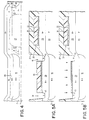
- a pad oxide 31 of 250 Angström is grown on the surface of the N- epi layer 29.
- a nitride layer 33 approximately 1000 Angström thick is deposited on the pad oxide 31 and a 5000 Angström layer 35 of oxide is deposited by CVD over the nitride. This stack is then patterned and selectively removed by photolithography to form the isolation pattern desired.
- an "n well" mask 37 (where NPN and PFET are located) is used to open those areas in the isolation stack where the PFET and NPN will be made.
- a guard ring implant (101 -1013 dose) is made, with the selection of implant energies so that only the edges of the device region 39 and 41 are doped. This guard ring 43 prevents leakage by enhancing the dopant concentration where the subsequent source/drain diffusions will butt the isolation oxide.
- the top CVD oxide 35 is removed (See Figure 5B) and the threshold adjust implant/punch-through protection implants are performed through the nitride 33 and pad oxide 31. In this process, a separate masking step to prevent the guard ring ion implant from influencing the threshold has been eliminated; in addition, the guard ring is self-aligned to the device area edge.
- the n-well resist 37 is then removed.
- Figure 6 shows the forming of the P well for the NFET and PNP.
- Resist 45 covers the n-well regions and a p type channel stop 47 is implanted into the field not doped by the n type guard ring but not into the nFET and PNP device regions.
- the purpose of the p type channel stop 47 is to prevent inversion of the surface due to a charge in the oxide or from the gate overlap of the thick oxide.
- the CVD oxide 35 on the p regions to be implanted is then selectively stripped away while leaving the P well resist mask 45 in place.
- the P well/V T adjust implants are performed and the n- epi is locally converted into P type 49A by these implants.
- the doping is such that during the field oxidation, the p well connects to the p type epi under the n-epi.
- the surface concentration is adjusted to attain the desired V T of the n FET.
- the field 51 is oxidized (5000 Angström - 6000 Angström ), the nitride 33 oxide 31 pad stack is removed and a gate oxide 53 (100 Angström - 150 Angström) is grown.
- the wafer is covered by a blanket deposition of a relatively thin (500 Angström - 600 Angström) layer 57 of LPCVD polysilicon. This layer acts to protect the gate oxide for the FET's while the oxide is removed for the formation of the bipolar transistors' emitters.
- a resist mask 59 is used for each type of bipolar device to define the area which will get the intrinsic base implant and the pedestal implant.
- the polysilicon 57 is etched selectively down to the gate oxide 53 (by RIE, e.g.).
- one type of pedestal 61 is implanted ( Figure 7A).
- the resist 59 is controllably etched-back; in this way the subsequent intrinsic base implant goes under the polysilicon layer 57 edge regions (and, therefore, past the emitter edge), to protect against punch-through as seen in Figure 7B.
- the etch back can either be done in a resist strip tool or a more directional RIE tool run at relatively high pressure.
- the process needs some degree of lateral etch so that the edge of the resist pulls back laterally, allowing the intrinsic base implant to go under the polysilicon. This yields a higher base dopant concentration at the emitter edge.
- the resist 59 is stripped, and the analogous process (not shown) occurs on the opposite type of bipolar, with a mask to define the intrinsic base and pedestal implants.
- the gate oxide acts as a screen oxide in both cases.
- the polysilicon emitter and FET gate electrodes can be formed. Since for the bipolar, the polysilicon must be in contact with single crystal silicon, the gate oxide 53 must be removed; but it must be kept for the FET's. As shown in Figure 8, this is resolved without a mask by using a dilute HF wet etch just prior to a second, thicker polysilicon deposition 65 (1500 Angström - 3000 Angström) to clean the surface. At the FET areas, however, the initial polysilicon 57 covers the gates and prevents the etchant from damaging them. The etch clears off the surface of the polysilicon of any native oxide, so the next layer makes good contact to the previous polysilicon. Alternate masking 75 is now used to dope the polysilicon as appropriate for emitter gates 67 and 71 of npn/nFET (n type) and gates 69 and 73 of pnp/pFET (p type).
- a silicide 77 (e.g., WSi2 or TiSi2) is formed on the polysilicon 65 and a CVD oxide or intrinsic polysilicon 79 is used to cap the silicide 77.
- the gate/emitter stacks 81, 83, 85, and 87 are then patterned by directional etching.
- the gate polysilicon is thicker than the emitter polysilicon (by the initial protective polysilicon 57) the single crystal silicon around the emitter will be etched. This will increase the distance between the emitter and the extrinsic base, so that the reverse breakdown voltage of the emitter-base junction will not be unacceptably low.
- oxidation and CVD oxide deposition (along with RIE) is used to form a spacer 91 approximately (300 Angström - 1000 Angström) at the edges of the emitter/gate.
- This oxide 91 acts as a spacer to offset the source/drain and extrinsic base implants from the edges of the gate/emitter. In the case of FET's, it prevents damage by the implants from impinging on the gate edge; for the bipolar, it moves the extrinsic base implant away from the emitter edge so the two high concentration regions do not touch and cause unacceptably low reverse breakdown.
- Two masks can now be used to selectively: 1) implant the p+ source/drain 93/95 and extrinsic base 97 of the pnp/pFET; and 2) implant the n+ source/drain 97/99 and extrinsic base 101 of the nFET/npn. If the spacing for the p+ to gate/emitter edge is to be different from the n+ to gate/emitter edge, one type implant can be done and then a second spacer formation process can be undertaken by CVD oxide deposition and RIE; this increases the source/drain (or extrinsic base) to gate/emitter edge spacing. Now the second source/drain implant can be done.
- the oxide and silicide on top of the gate/emitter polysilicon prevents the source/drain dopant from counter doping the polysilicon.
- a drive-in will finish the processing.
- the reach-through 103 to the N+ subcollector is made the same way as the npn extrinsic base 97 adjacent to the emitter in that the reach-through gets a N+ implant using the source/drain mask. This N+ implant (instead of a P+ implant) counterdopes the base implant.
- the reach-through to the P+ subcollector is made by using the non-emitter pnp base region doped with the p+ source/drain implant (not shown in Figure 11). No extra processing is needed to form the reach-through.
Landscapes
- Metal-Oxide And Bipolar Metal-Oxide Semiconductor Integrated Circuits (AREA)
- Bipolar Transistors (AREA)
- Bipolar Integrated Circuits (AREA)
Claims (11)
- Processus de production simultanée de transistors bipolaires NPN et PNP verticaux et de transistors à effet de champ complémentaires sur une première couche (3) épitaxiale dopée P commune mise en croissance sur un substrat de semi-conducteur (1), dans lequel des zones (15, 17) de subcollecteur N+ à couche épitaxiale sont formées à des emplacements sélectionnés, lesdites zones de subcollecteur sont oxydées à une hauteur différente dans le but d'aligner des masques ultérieurs et dans ladite couche épitaxiale, des zones (27) de subcollecteur P+ sont également formées à des emplacements sélectionnés afin de procurer une ligne à faible résistance vers le substrat, ledit processus comprenant les étapes consistant à :a) mettre en croissance une seconde couche (29) épitaxiale et mettre en croissance/déposer un oxyde de plot (31) et une couche de nitrure (33) sur la surface de ladite seconde couche épitaxiale (29) et déposer une couche d'oxyde (35) sur ladite couche de nitrure,b) mettre en motif ladite couche d'oxyde/nitrure/oxyde afin d'exposer les zones d'isolement de surface,c) définir des régions à puits n avec un masque (37) de façon à ce qu'elles contiennent une partie de la seconde couche épitaxiale (29) exposée pendant l'étape b),d) implanter un dopant du type n sur les régions exposées afin de former un anneau de garde du dispositif,e) éliminer ladite couche d'oxyde exposée (35) et implanter un dopant de type n afin de régler la tension de seuil,f) éliminer ledit masque de puits n (37) et répéter les étapes c) à e) pour les régions à puits p pour les n/FET et PNP en remplaçant le dopant de type p par le dopant de type n, et éliminer alors le masque de puits p (45),g) réaliser une oxydation afin de former l'oxyde de champ (51), en éliminant la couche d'oxyde nitrure/plot et en mettant à croître une couche d'oxyde de grille (53),h) déposer une couche en couverture (57) de polysilicium par dépôt chimique en phase vapeur sous basse pression,i) masquer ledit polysilicium avec un masque (59) et graver de façon sélective ledit polysilicium jusqu'à l'oxyde de grille dans la région d'émetteur bipolaire et la région de traversée d'accès au collecteur,j) implanter un collecteur de piédestal du type n dans lesdits emplacements ouverts,k) graver à nouveau ledit masque (59),l) implanter un dopant de type P dans le puits de base bipolaire,m) éliminer ledit masque (59),n) répéter les étapes g) à m) pour le type opposé de dispositif bipolaire en remplaçant le dopant de type p par le dopant de type n,o) éliminer partiellement la couche d'oxyde de grille (53),p) déposer une seconde couche (65) de polysilicium sur la surface,q) doper ladite seconde couche de polysilicium (65),r) mettre en motif ladite seconde couche de polysilicium (65) afin de former les électrodes de grille et les contacts d'émetteur en polysilicium, ce par quoi un évidement est produit à la surface contiguë aux contacts d'émetteur, et,s) former les régions respectives de traversée d'accès de type p et de type n, de base extrinsèque, et de source et de drain en utilisant des masques de photorésist et en implantant le dopant respectif dans les régions prédéterminées.
- Processus selon la revendication 1 dans lequel ladite couche d'oxyde/nitrure/oxyde est respectivement, d'une épaisseur d'approximativement 25 nm, 100 nm et 500 nm.
- Processus selon la revendication 2 dans lequel ledit anneau de garde comporte une concentration en dopant de 10⁻¹ à 10⁻¹³ cm⁻.
- Processus selon la revendication 3 dans lequel le champ est oxydé jusqu'à une épaisseur d'approximativement 500 à 600 nm et l'oxyde de grille est d'une épaisseur de 10 à 15, le dépôt de couverture de polysilicium par dépôt chimique en phase vapeur à basse pression est de 50 à 60 nm d'épaisseur, le polysilicium est gravé de façon sélective par une gravure à ions réactifs, le résist de masquage du polysilicium est regravé soit au moyen d'un outil de dénudage de résist, soit d'un outil de gravure par ions réactifs et dans lequel l'oxyde de grille est éliminé par un acide fluorhydrique dilué.
- Processus selon la revendication 4 dans lequel le second dépôt de polysilicium plus épais est d'une épaisseur de 150 à 300 nm.
- Processus selon la revendication 5 dans lequel, sur la seconde couche de polysilicium, est située une couche d'un siliciure suivie d'une couche d'un oxyde par dépôt chimique en phase vapeur et le siliciure est du siliciure de tungstène ou du siliciure de titane.
- Processus selon la revendication 6 dans lequel les empilements d'électrodes de grille et les empilements d'électrodes d'émetteur sont mis en motif par une élimination sélective du polysilicium, l'élimination étant effectuée par une gravure à ions réactifs.
- Processus selon la revendication 7 dans lequel une couche d'espacement d'oxyde est formée aux limites du contact d'émetteur et du contact de grille, cette couche d'oxyde étant d'une épaisseur de 30 à 100 nm.
- Processus selon la revendication 8 dans lequel deux implantations d'ions sont faites pour former la source/drain P+ et la base extrinsèque du PNP/PFET et la source/drain n+ et la base extrinsèque du nFET/NPN.
- Processus selon la revendication 8 dans lequel une seconde couche d'espacement d'oxyde est -formée aux limites du contact d'émetteur et du contact de grille qui peut alors être suivie d'implantations d'ions afin de former les régions de source/drain et de base.
- Processus selon la revendication 1 dans lequel le subcollecteur P+ est isolé du substrat par un oxyde formé par de l'oxygène d'implantation ionique ou par l'utilisation d'une couche épitaxiale de type N.
Applications Claiming Priority (2)
| Application Number | Priority Date | Filing Date | Title |
|---|---|---|---|
| US07/287,945 US4868135A (en) | 1988-12-21 | 1988-12-21 | Method for manufacturing a Bi-CMOS device |
| US287945 | 1988-12-21 |
Publications (3)
| Publication Number | Publication Date |
|---|---|
| EP0375585A2 EP0375585A2 (fr) | 1990-06-27 |
| EP0375585A3 EP0375585A3 (fr) | 1991-04-10 |
| EP0375585B1 true EP0375585B1 (fr) | 1996-04-10 |
Family
ID=23105052
Family Applications (1)
| Application Number | Title | Priority Date | Filing Date |
|---|---|---|---|
| EP89480174A Expired - Lifetime EP0375585B1 (fr) | 1988-12-21 | 1989-11-07 | Procédé pour fabriquer un dispositif du type BICMOS |
Country Status (4)
| Country | Link |
|---|---|
| US (1) | US4868135A (fr) |
| EP (1) | EP0375585B1 (fr) |
| JP (1) | JPH0744232B2 (fr) |
| DE (1) | DE68926224T2 (fr) |
Families Citing this family (58)
| Publication number | Priority date | Publication date | Assignee | Title |
|---|---|---|---|---|
| US4929565A (en) * | 1986-03-04 | 1990-05-29 | Motorola, Inc. | High/low doping profile for twin well process |
| US4897703A (en) * | 1988-01-29 | 1990-01-30 | Texas Instruments Incorporated | Recessed contact bipolar transistor and method |
| US5075241A (en) * | 1988-01-29 | 1991-12-24 | Texas Instruments Incorporated | Method of forming a recessed contact bipolar transistor and field effect device |
| JPH02101747A (ja) * | 1988-10-11 | 1990-04-13 | Toshiba Corp | 半導体集積回路とその製造方法 |
| US5028977A (en) * | 1989-06-16 | 1991-07-02 | Massachusetts Institute Of Technology | Merged bipolar and insulated gate transistors |
| EP0417457A3 (en) * | 1989-08-11 | 1991-07-03 | Seiko Instruments Inc. | Method of producing field effect transistor |
| EP0436297A3 (en) * | 1989-12-04 | 1992-06-17 | Raytheon Company | Small bicmos transistor |
| US4997775A (en) * | 1990-02-26 | 1991-03-05 | Cook Robert K | Method for forming a complementary bipolar transistor structure including a self-aligned vertical PNP transistor |
| US5102811A (en) * | 1990-03-20 | 1992-04-07 | Texas Instruments Incorporated | High voltage bipolar transistor in BiCMOS |
| US5104817A (en) * | 1990-03-20 | 1992-04-14 | Texas Instruments Incorporated | Method of forming bipolar transistor with integral base emitter load resistor |
| EP0452720A3 (en) * | 1990-04-02 | 1994-10-26 | Nat Semiconductor Corp | A semiconductor structure and method of its manufacture |
| JPH0445538A (ja) * | 1990-06-13 | 1992-02-14 | Oki Electric Ind Co Ltd | 半導体装置の製造方法 |
| US5001073A (en) * | 1990-07-16 | 1991-03-19 | Sprague Electric Company | Method for making bipolar/CMOS IC with isolated vertical PNP |
| KR970000425B1 (ko) * | 1990-09-20 | 1997-01-09 | 이해욱 | BiCMOS형 전계효과 트랜지스터 및 그의 제조방법 |
| KR940003589B1 (ko) * | 1991-02-25 | 1994-04-25 | 삼성전자 주식회사 | BiCMOS 소자의 제조 방법 |
| EP0505877A2 (fr) * | 1991-03-27 | 1992-09-30 | Seiko Instruments Inc. | Méthode de dopage à l'aide d'une source de diffusion adsorbée |
| US5101257A (en) * | 1991-07-01 | 1992-03-31 | Motorola, Inc. | Semiconductor device having merged bipolar and MOS transistors and process for making the same |
| US5132236A (en) * | 1991-07-30 | 1992-07-21 | Micron Technology, Inc. | Method of semiconductor manufacture using an inverse self-aligned mask |
| KR940007466B1 (ko) * | 1991-11-14 | 1994-08-18 | 삼성전자 주식회사 | BiCMOS 소자의 제조방법 |
| US5306652A (en) * | 1991-12-30 | 1994-04-26 | Texas Instruments Incorporated | Lateral double diffused insulated gate field effect transistor fabrication process |
| WO1993016494A1 (fr) * | 1992-01-31 | 1993-08-19 | Analog Devices, Inc. | Dispositifs emetteurs bipolaires complementaires en polysilicium |
| US5164326A (en) * | 1992-03-30 | 1992-11-17 | Motorola, Inc. | Complementary bipolar and CMOS on SOI |
| US5286991A (en) * | 1992-08-26 | 1994-02-15 | Pioneer Semiconductor Corporation | Capacitor for a BiCMOS device |
| US5504363A (en) * | 1992-09-02 | 1996-04-02 | Motorola Inc. | Semiconductor device |
| US6011283A (en) * | 1992-10-19 | 2000-01-04 | Hyundai Electronics America | Pillar emitter for BiCMOS devices |
| US5557131A (en) * | 1992-10-19 | 1996-09-17 | At&T Global Information Solutions Company | Elevated emitter for double poly BICMOS devices |
| US5384278A (en) * | 1992-11-16 | 1995-01-24 | United Technologies Corporation | Tight control of resistor valves in a SRAM process |
| US6249030B1 (en) | 1992-12-07 | 2001-06-19 | Hyundai Electronics Industries Co., Ltd. | BI-CMOS integrated circuit |
| US5516718A (en) * | 1992-12-07 | 1996-05-14 | At&T Global Information Solutions Company | Method of making BI-CMOS integrated circuit having a polysilicon emitter |
| JP3343968B2 (ja) * | 1992-12-14 | 2002-11-11 | ソニー株式会社 | バイポーラ型半導体装置およびその製造方法 |
| US5411900A (en) * | 1993-03-05 | 1995-05-02 | Deutsche Itt Industries, Gmbh | Method of fabricating a monolithic integrated circuit with at least one CMOS field-effect transistor and one NPN bipolar transistor |
| DE4319437C1 (de) * | 1993-03-05 | 1994-05-19 | Itt Ind Gmbh Deutsche | Verfahren zur Herstellung einer monolithisch integrierten Schaltung mit mindestens einem CMOS-Feldeffekttransistor und einem npn-Bipolar-Transistor |
| US5448085A (en) * | 1993-04-05 | 1995-09-05 | The United States Of America As Represented By The Secretary Of The Air Force | Limited current density field effect transistor with buried source and drain |
| US5441903A (en) * | 1993-12-03 | 1995-08-15 | Texas Instruments Incorporated | BiCMOS process for supporting merged devices |
| JPH07169771A (ja) * | 1993-12-15 | 1995-07-04 | Nec Corp | 半導体装置及びその製造方法 |
| US5444004A (en) * | 1994-04-13 | 1995-08-22 | Winbond Electronics Corporation | CMOS process compatible self-alignment lateral bipolar junction transistor |
| DE19523536A1 (de) * | 1994-07-12 | 1996-01-18 | Siemens Ag | Verfahren zur Herstellung von MOS-Transistoren und Bipolartransistoren auf einer Halbleiterscheibe |
| JPH08107114A (ja) * | 1994-10-04 | 1996-04-23 | Mitsubishi Electric Corp | 半導体装置およびその製造方法 |
| US5449627A (en) * | 1994-12-14 | 1995-09-12 | United Microelectronics Corporation | Lateral bipolar transistor and FET compatible process for making it |
| US5627097A (en) * | 1995-07-03 | 1997-05-06 | Motorola, Inc. | Method for making CMOS device having reduced parasitic capacitance |
| JP2790084B2 (ja) * | 1995-08-16 | 1998-08-27 | 日本電気株式会社 | 半導体装置の製造方法 |
| RU2106039C1 (ru) * | 1995-11-09 | 1998-02-27 | Акционерное общество открытого типа "НИИМЭ и завод "Микрон" | Способ изготовления бикмоп структур |
| US5786622A (en) * | 1997-05-16 | 1998-07-28 | Tritech Microelectronics International Ltd. | Bipolar transistor with a ring emitter |
| US5882977A (en) * | 1997-10-03 | 1999-03-16 | International Business Machines Corporation | Method of forming a self-aligned, sub-minimum isolation ring |
| US6096618A (en) * | 1998-01-20 | 2000-08-01 | International Business Machines Corporation | Method of making a Schottky diode with sub-minimum guard ring |
| US6246096B1 (en) * | 1998-06-24 | 2001-06-12 | Advanced Micro Devices | Totally self-aligned transistor with tungsten gate |
| WO2003038893A2 (fr) * | 2001-10-26 | 2003-05-08 | Infineon Technologies Ag | Structure a semi-conducteur et procede de fabrication de ladite structure |
| US6762469B2 (en) * | 2002-04-19 | 2004-07-13 | International Business Machines Corporation | High performance CMOS device structure with mid-gap metal gate |
| US7037799B2 (en) * | 2002-10-24 | 2006-05-02 | Texas Instruments Incorporated | Breakdown voltage adjustment for bipolar transistors |
| US6909164B2 (en) * | 2002-11-25 | 2005-06-21 | International Business Machines Corporation | High performance vertical PNP transistor and method |
| JP4845410B2 (ja) * | 2005-03-31 | 2011-12-28 | 株式会社リコー | 半導体装置 |
| JP4342579B2 (ja) * | 2006-08-31 | 2009-10-14 | 三洋電機株式会社 | 半導体装置 |
| JP2009010341A (ja) * | 2007-05-29 | 2009-01-15 | Toshiba Corp | 半導体装置の製造方法 |
| US8211786B2 (en) | 2008-02-28 | 2012-07-03 | International Business Machines Corporation | CMOS structure including non-planar hybrid orientation substrate with planar gate electrodes and method for fabrication |
| US7687862B2 (en) * | 2008-05-13 | 2010-03-30 | Infineon Technologies Ag | Semiconductor devices with active regions of different heights |
| CN103426759B (zh) * | 2012-05-16 | 2016-02-10 | 上海华虹宏力半导体制造有限公司 | Pldmos的制造方法 |
| JP6219224B2 (ja) * | 2014-04-21 | 2017-10-25 | ルネサスエレクトロニクス株式会社 | 半導体装置 |
| US12513941B2 (en) * | 2022-06-24 | 2025-12-30 | Vanguard International Semiconductor Corporation | Semiconductor device and method for forming the same |
Family Cites Families (7)
| Publication number | Priority date | Publication date | Assignee | Title |
|---|---|---|---|---|
| US4403395A (en) * | 1979-02-15 | 1983-09-13 | Texas Instruments Incorporated | Monolithic integration of logic, control and high voltage interface circuitry |
| US4637125A (en) * | 1983-09-22 | 1987-01-20 | Kabushiki Kaisha Toshiba | Method for making a semiconductor integrated device including bipolar transistor and CMOS transistor |
| US4553315A (en) * | 1984-04-05 | 1985-11-19 | Harris Corporation | N Contact compensation technique |
| US4696092A (en) * | 1984-07-02 | 1987-09-29 | Texas Instruments Incorporated | Method of making field-plate isolated CMOS devices |
| DE3680520D1 (de) * | 1986-03-22 | 1991-08-29 | Itt Ind Gmbh Deutsche | Verfahren zum herstellen einer monolithisch integrierten schaltung mit mindestens einem bipolaren planartransistor. |
| JPS6329967A (ja) * | 1986-07-24 | 1988-02-08 | Fuji Xerox Co Ltd | 半導体装置の製造方法 |
| US4784966A (en) * | 1987-06-02 | 1988-11-15 | Texas Instruments Incorporated | Self-aligned NPN bipolar transistor built in a double polysilicon CMOS technology |
-
1988
- 1988-12-21 US US07/287,945 patent/US4868135A/en not_active Expired - Fee Related
-
1989
- 1989-11-07 EP EP89480174A patent/EP0375585B1/fr not_active Expired - Lifetime
- 1989-11-07 DE DE68926224T patent/DE68926224T2/de not_active Expired - Fee Related
- 1989-12-20 JP JP1328605A patent/JPH0744232B2/ja not_active Expired - Lifetime
Also Published As
| Publication number | Publication date |
|---|---|
| US4868135A (en) | 1989-09-19 |
| EP0375585A2 (fr) | 1990-06-27 |
| JPH0744232B2 (ja) | 1995-05-15 |
| JPH02215158A (ja) | 1990-08-28 |
| DE68926224D1 (de) | 1996-05-15 |
| EP0375585A3 (fr) | 1991-04-10 |
| DE68926224T2 (de) | 1996-10-10 |
Similar Documents
| Publication | Publication Date | Title |
|---|---|---|
| EP0375585B1 (fr) | Procédé pour fabriquer un dispositif du type BICMOS | |
| US6686233B2 (en) | Integration of high voltage self-aligned MOS components | |
| US5424572A (en) | Spacer formation in a semiconductor structure | |
| US5428243A (en) | Bipolar transistor with a self-aligned heavily doped collector region and base link regions. | |
| US4962053A (en) | Bipolar transistor fabrication utilizing CMOS techniques | |
| US6271575B1 (en) | Method and mask structure for self-aligning ion implanting to form various device structures | |
| KR20010087183A (ko) | 폴리-폴리 캐패시터, mos 트랜지스터 및 바이폴라트랜지스터의 동시 형성 방법, 폴리-폴리 캐패시터 및 그제조 방법 | |
| EP0768709B1 (fr) | Procédé BiCMOS avec transistor bipolaire ayant un faible courant de recombinaison de base | |
| US6461925B1 (en) | Method of manufacturing a heterojunction BiCMOS integrated circuit | |
| EP0281235B1 (fr) | Procédé pour fabriquer un transistor bipolaire utilisant des technologies de type CMOS | |
| US5010034A (en) | CMOS and bipolar fabrication process using selective epitaxial growth scalable to below 0.5 micron | |
| US5504364A (en) | CMOS locos isolation for self-aligned NPN BJT in a BiCMOS process | |
| US5065209A (en) | Bipolar transistor fabrication utilizing CMOS techniques | |
| US6790736B2 (en) | Method for manufacturing and structure of semiconductor device with polysilicon definition structure | |
| US6080612A (en) | Method of forming an ultra-thin SOI electrostatic discharge protection device | |
| EP0434182B1 (fr) | Procédé de fabrication de couches enterrées pour circuits intégrés | |
| US6100124A (en) | Method for manufacturing a BiCMOS semiconductor device | |
| US6383855B1 (en) | High speed, low cost BICMOS process using profile engineering | |
| US6033232A (en) | Process of fabricating photodiode integrated with MOS device | |
| JP3247106B2 (ja) | 集積回路の製法と集積回路構造 | |
| JPH11121639A (ja) | N形ウエル補償注入が行われたBiCMOS集積回路とその製造法 | |
| JP2918205B2 (ja) | 半導体装置およびその製造方法 | |
| EP0366967B1 (fr) | Une méthode de fabrication de circuits intégrés ayant des régions dopées enternées | |
| KR20010057342A (ko) | 반도체장치의 제조방법 | |
| KR20020034561A (ko) | 반도체장치 및 그 제조방법 |
Legal Events
| Date | Code | Title | Description |
|---|---|---|---|
| PUAI | Public reference made under article 153(3) epc to a published international application that has entered the european phase |
Free format text: ORIGINAL CODE: 0009012 |
|
| AK | Designated contracting states |
Kind code of ref document: A2 Designated state(s): DE FR GB |
|
| 17P | Request for examination filed |
Effective date: 19901025 |
|
| PUAL | Search report despatched |
Free format text: ORIGINAL CODE: 0009013 |
|
| AK | Designated contracting states |
Kind code of ref document: A3 Designated state(s): DE FR GB |
|
| 17Q | First examination report despatched |
Effective date: 19930920 |
|
| GRAA | (expected) grant |
Free format text: ORIGINAL CODE: 0009210 |
|
| AK | Designated contracting states |
Kind code of ref document: B1 Designated state(s): DE FR GB |
|
| PG25 | Lapsed in a contracting state [announced via postgrant information from national office to epo] |
Ref country code: FR Effective date: 19960410 |
|
| REF | Corresponds to: |
Ref document number: 68926224 Country of ref document: DE Date of ref document: 19960515 |
|
| EN | Fr: translation not filed | ||
| PG25 | Lapsed in a contracting state [announced via postgrant information from national office to epo] |
Ref country code: GB Effective date: 19961107 |
|
| PLBE | No opposition filed within time limit |
Free format text: ORIGINAL CODE: 0009261 |
|
| STAA | Information on the status of an ep patent application or granted ep patent |
Free format text: STATUS: NO OPPOSITION FILED WITHIN TIME LIMIT |
|
| 26N | No opposition filed | ||
| GBPC | Gb: european patent ceased through non-payment of renewal fee |
Effective date: 19961107 |
|
| PG25 | Lapsed in a contracting state [announced via postgrant information from national office to epo] |
Ref country code: DE Effective date: 19970801 |