EP0376311A2 - Elément photosensible pour électrophotographie - Google Patents
Elément photosensible pour électrophotographie Download PDFInfo
- Publication number
- EP0376311A2 EP0376311A2 EP89124079A EP89124079A EP0376311A2 EP 0376311 A2 EP0376311 A2 EP 0376311A2 EP 89124079 A EP89124079 A EP 89124079A EP 89124079 A EP89124079 A EP 89124079A EP 0376311 A2 EP0376311 A2 EP 0376311A2
- Authority
- EP
- European Patent Office
- Prior art keywords
- charge
- layer
- substituent
- member according
- group capable
- Prior art date
- Legal status (The legal status is an assumption and is not a legal conclusion. Google has not performed a legal analysis and makes no representation as to the accuracy of the status listed.)
- Granted
Links
Images

Classifications
-
- G—PHYSICS
- G03—PHOTOGRAPHY; CINEMATOGRAPHY; ANALOGOUS TECHNIQUES USING WAVES OTHER THAN OPTICAL WAVES; ELECTROGRAPHY; HOLOGRAPHY
- G03G—ELECTROGRAPHY; ELECTROPHOTOGRAPHY; MAGNETOGRAPHY
- G03G5/00—Recording-members for original recording by exposure, e.g. to light, to heat or to electrons; Manufacture thereof; Selection of materials therefor
- G03G5/02—Charge-receiving layers
- G03G5/04—Photoconductive layers; Charge-generation layers or charge-transporting layers; Additives therefor; Binders therefor
- G03G5/06—Photoconductive layers; Charge-generation layers or charge-transporting layers; Additives therefor; Binders therefor characterised by the photoconductive material being organic
- G03G5/0622—Heterocyclic compounds
- G03G5/0624—Heterocyclic compounds containing one hetero ring
- G03G5/0635—Heterocyclic compounds containing one hetero ring being six-membered
- G03G5/0637—Heterocyclic compounds containing one hetero ring being six-membered containing one hetero atom
-
- G—PHYSICS
- G03—PHOTOGRAPHY; CINEMATOGRAPHY; ANALOGOUS TECHNIQUES USING WAVES OTHER THAN OPTICAL WAVES; ELECTROGRAPHY; HOLOGRAPHY
- G03G—ELECTROGRAPHY; ELECTROPHOTOGRAPHY; MAGNETOGRAPHY
- G03G5/00—Recording-members for original recording by exposure, e.g. to light, to heat or to electrons; Manufacture thereof; Selection of materials therefor
- G03G5/02—Charge-receiving layers
- G03G5/04—Photoconductive layers; Charge-generation layers or charge-transporting layers; Additives therefor; Binders therefor
- G03G5/06—Photoconductive layers; Charge-generation layers or charge-transporting layers; Additives therefor; Binders therefor characterised by the photoconductive material being organic
- G03G5/0601—Acyclic or carbocyclic compounds
- G03G5/0612—Acyclic or carbocyclic compounds containing nitrogen
- G03G5/0614—Amines
- G03G5/06142—Amines arylamine
-
- G—PHYSICS
- G03—PHOTOGRAPHY; CINEMATOGRAPHY; ANALOGOUS TECHNIQUES USING WAVES OTHER THAN OPTICAL WAVES; ELECTROGRAPHY; HOLOGRAPHY
- G03G—ELECTROGRAPHY; ELECTROPHOTOGRAPHY; MAGNETOGRAPHY
- G03G5/00—Recording-members for original recording by exposure, e.g. to light, to heat or to electrons; Manufacture thereof; Selection of materials therefor
- G03G5/02—Charge-receiving layers
- G03G5/04—Photoconductive layers; Charge-generation layers or charge-transporting layers; Additives therefor; Binders therefor
- G03G5/06—Photoconductive layers; Charge-generation layers or charge-transporting layers; Additives therefor; Binders therefor characterised by the photoconductive material being organic
- G03G5/0622—Heterocyclic compounds
- G03G5/0624—Heterocyclic compounds containing one hetero ring
- G03G5/0627—Heterocyclic compounds containing one hetero ring being five-membered
- G03G5/0629—Heterocyclic compounds containing one hetero ring being five-membered containing one hetero atom
Definitions
- the present invention relates to a photosensitive member for electrophotography, particularly to a photosensitive member for electrophotography comprising a low-molecular weight organic photoconductor capable of providing improved electrophotographic characteristics.
- organic photoconductive polymers to be used for electrophotographic photosensitive members, such as polyvinyl carbazole.
- These conventional organic polymers are superior to inorganic photoconductive materials in lightness (in weight), film-forming property, etc., but are inferior to the latter in sensitivity, durability, stability to environmental change, mechanical strength, etc.
- the conventional low-molecular weight organic photoconductors represented by those as described above are used, the above-mentioned defect in film-forming property, which has conventionally posed a problem in the field of the organic photoconductive polymer, may be obviated by appropriately selecting a binder to be used in combination therewith.
- these conventional organic photoconductors cannot provide a sufficient sensitivity.
- the electrophotographic photosensitive member comprising such a photosensitive layer may be improved in sensitivity to visible light, charge retentivity, surface strength, etc.
- organic compounds As the charge-transporting substance constituting the above-mentioned charge transport layer, a large number of organic compounds have heretofore been proposed. Examples thereof include: pyrazoline compounds (Japanese Laid-Open Patent Application No. 72231/1977), hydrazone compounds (U.S. Patent 842,431 and Japanese Laid-Open Patent Application No. 52063/1980), triphenylamine compounds (Japanese Laid-Open Patent Application Nos. 195254/1982 and 58445/1979), stilbene compounds (Japanese Laid-Open Patent Application Nos. 151955/1979 and 198043/1983), carbazole compounds (Japanese Laid-Open Patent Application Nos. 150128/1979 and 58451/1988), benzothiophene compounds (Japanese Laid-Open Patent Application No. 110835/1979), etc.
- pyrazoline compounds Japanese Laid-Open Patent Application No. 72231/1977
- hydrazone compounds U.S. Patent
- the sensitivity and other electrophotographic characteristics are not necessarily sufficient, and the light part potential and dark part potential are liable to show a considerable change, when charging and exposure operations are conducted repetitively.
- An object of the present invention is to provide an electrophotographic photosensitive member which has solved the above-mentioned various problems encountered in the conventional photosensitive member.
- Another object of the present invention is to provide an electrophotographic photosensitive member using a novel organic photoconductor which may easily be produced, is relatively inexpensive and is excellent in durability.
- a photosensitive member for electrophotography comprising an electroconductive substrate and a photosensitive layer disposed thereon, wherein the photosensitive layer comprises a triarylamine compound represented by the following general formula (I) or (II): wherein Ar, and Ar 2 respectively denote a biphenyl group capable of having a substituent; Ara denotes a phenyl group capable of having a substituent or an aromatic heterocyclic group capable of having a substituent; Ar4 and Ar 5 respectively denote a benzene ring or aromatic fused-ring hydrocarbon group capable of having a substituent; R 1 and R 2 respectively denote a hydrogen atom, alkyl, alkoxyl or halogen atom; and at least one of Ar4 and Ar s is an aromatic fused-ring hydrocarbon group.
- Ar, and Ar 2 respectively denote a biphenyl group capable of having a substituent
- Ara denotes a phenyl group capable of having a substituent or an aromatic heterocyclic group capable of having
- Ar, and Ar 2 respectively denote a biphenyl group capable of having a substituent.
- substituent may include alkyl groups such as methyl, ethyl and propyl; alkoxy groups such as methoxy, ethoxy and propoxy; halogen atoms such as fluorine, chlorine and bromine; etc.
- Ar may be the as or different from Ar 2 .
- Ar 3 denotes a phenyl group capable of having a substituent, or an aromatic heterocyclic group such as pyridyl, quinolyl, thienyl or furyl capable of having a substituent.
- a substituent may include: alkyl groups such as methyl, ethyl and propyl; alkoxy groups such as methoxy, ethoxy and propoxy; aryloxy groups such as phenoxy and naphthoxy; aromatic groups such as phenyl and naphthyl; halogen atoms such as fluorine, chlorine and bromine; etc.
- Ar 1 and Ar 2 respectively denote a benzene ring or aromatic condensed-ring (or fused-ring) hydrocarbon group capable of having a substituent. At least one of Ar l and Ar 2 is an aromatic condensed ring hydrocarbon group. Specific examples of such an aromatic condensed ring hydrocarbon may include naphthalene, anthracene, phenanthrene, chrysene and naphthacene.
- Ar 1 and Ar 2 may have include: alkyl groups such as methyl, ethyl and propyl; alkoxy groups such as methoxy, ethoxy and propoxy; halogen atoms such as fluorine, chlorine and bromine; etc.
- Ar may be the as or different from Ar 2 .
- R, and R 2 respectively denote a hydrogen atom; an alkyl group such as methyl, ethyl and propyl; an alkoxy group such as methoxy, ethoxy and propoxy; a halogen atom such as fluorine, chlorine and bromine; etc.
- R may be the as or different from R 2 .
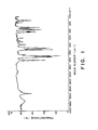
- Figure 1 shows an infrared absorption spectrum chart obtained by measuring the thus obtained compound by a KBr tablet (or pellet) method.
- Figure 2 shows an infrared absorption spectrum chart obtained by measuring the thus obtained compound by a KBr tablet (or pellet) method.
- the compound according to the present invention may easily be synthesized inexpensively.
- the other compounds according to the present invention may be synthesized in a similar manner as described in the above-mentioned Synthesis Examples.
- the photosensitive layer is function- separated into a charge generation layer and a charge transport layer, and the charge transport layer comprises the compound represented by the above-mentioned general formula (I) or (II) as a charge-transporting substance.
- the charge transport layer according to the present invention may preferably be formed by dissolving the above-mentioned compound of the formula (I) or (II) in an appropriate solvent together with a binder, applying the resultant coating liquid such as solution onto a predetermined surface, and drying the resultant coating.
- binder to be used for forming the charge transport layer may include; polyarylate resins, polysulfone resins, polyamide resins, acrylic resins, acrylonitrile resins, methacrylic resins, vinyl chloride resins, vinyl acetate resins, phenol resins, epoxy resins, polyester resins, alkyd resins, polycarbonate, polyurethane, or copolymer resins containing two or more of the recurring units of these resins, such as styrene-butadiene copolymers, styrene-acrylonitrile copolymers, styrene-maleic acid copolymers, etc.
- organic photoconductive polymers such as polyvinylcar- apelole, polyvinylanthracene and polyvinylpyrene may be used.
- the charge- transporting substance may preferably be used in an amount of 10 - 500 wt. parts, more preferably 50 - 200 wt. parts, per 100 wt. parts of the binder.
- the charge transport layer is electrically connected to the charge generation layer as described hereinafter, and has a function of receiving charge carriers injected from the charge generation layer in the presence of an electric field and of transporting these charge carriers to the surface of the charge transport layer.
- the charge transport layer may be disposed on the charge generation layer, or may be disposed under the charge generation layer.
- the charge transport layer may preferably be disposed on the charge generation layer. It is not preferred that the charge transport layer has too large a thickness, since there is a certain limit to the thickness thereof suitable for the transport of the charge carriers.
- the charge transport layer may preferably have a thickness of 5 - 40 microns, more preferably 10 - 30 microns.
- the organic solvent to be used in the above-mentioned formation of the charge transport layer may vary depending on the kind of the binder used therefor, and may preferably be selected from those which do not substantially dissolve the charge generation layer or a primer (or undercoat layer) as described hereinafter.
- organic solvent may include: alcohols such as methanol, ethanol, and isopropanol; ketones such as acetone, methyl ethyl ketone, and cyclohexanone; amides such as N,N-dimethylformamide and N,N-dimethylacetamide; sulfoxides such as dimethyl sulfoxide; ethers such as tetrahydrofuran, dioxane, and ethylene glycol monomethyl ether; esters such as methyl acetate and ethyl acetate; aliphatic halogenated hydrocarbons such as chloroform, methylene chloride, dichloroethylene, carbon tetrachloride, and trichloroethylene; aromatic compounds such as benzene, toluene, xylene, monochlorobenzene, and dichlorobenzene; etc.
- alcohols such as methanol, ethanol, and isopropanol
- ketones such as acetone
- the coating may be effected by various coating methods such as dip coating, spray coating, wire bar coating, and blade coating.
- the drying should preferably be conducted in the sequence of drying at room temperature to a "tack-free" state and then heat drying. In general, the heat drying may preferably be conducted for a time in the range of 5 minutes to 2 hours at a temperature of 30 ° C to 200 ° C under quiescent condition or under blowing.
- the charge transport layer according to the present invention can further contain an additive selected from various species thereof.
- an additive may include: plasticizers such as diphenyl, m-terphenyl and dibutyl phthalates; surface-lubricating agents such as silicone oil, graft-type silicone polymers, and various fluorocarbons; potential stabilizing agents such as dicyanovinyl compounds and carbazole derivatives; anti-oxidizing agents such as ,a-carotene, Ni complexes, and 1,4-diazabicyclo[2,2,2]-octane; etc.
- the charge generation layer may comprise a charge-generating substance.
- the charge-generating substance may include: inorganic charge-generating substances such as selenium, selenium-tellurium, and amorphous silicon; and organic charge-generating substances including: cationic dyes such as pyrylium dye, thiapyrylium dye, azulenium dye, thiacyanine dye, and quinocyanine dye; polycyclic quinone pigments such as squarium salt dye, phthalocyanine pigment, anthanthrone pigment, dibenzpyrene-quinone pigment, and pyranthrone pigment; indigo pigment; quinacridone pigment; azo pigment; etc.
- These charge-generating substances may be used singly or as a combination of two or more species.
- the charge generation layer may be formed by using such a charge-generating substance in the form of a vapor deposition layer or coating layer.
- the azo pigment particularly includes various types. Representative structures of the azo pigment preferably used in the present invention are described hereinbelow. When the azo pigment is represented by a general formula including the following central skeleton A:
- coupler portion Cp include those having the following structures:
- the above-mentioned central skeleton A and coupler Cp may appropriately be combined to form a pigment as a charge-generating substance.
- the charge generation layer may be formed by vapor-depositing such a charge-generating substance by means of a vacuum vapor deposition device, or by applying a dispersion containing such a charge-generating substance dispersed therein, together with an appropriate binder as desired.
- the binder to be used for forming the charge generation layer may be selected from a wide variety of insulating resins or alternatively from organic photoconductive polymers such as poly-N-vinylcarbazole, polyvinylanthracene, and polyvinylpyrene.
- the insulating resin such as polyvinyl butyral, polyarylates (e.g., polycondensation product between bisphenol A and phthalic acid), polycarbonate, polyester, phenoxy resin, acrylic resin, polyacrylamide resin, polyamide, polyvinyl pyridine, cellulose resin, urethane resin, epoxy resin, casein, polyvinyl alcohol, and polyvinyl pyrrolidone.
- the resin may preferably be contained in the charge generation layer in an amount of 5 - 80 wt. %, more preferably 10 - 40 wt. %.
- organic solvent usable in the coating of the charge generation layer may include: alcohols such as methanol, ethanol, and isopropanol; ketones such as acetone, methyl ethyl ketone, and cyclohexanone; amides such as N,N-dimethylformamide and N,N-dimethylacetamide; sulfoxides such as dimethyl sulfoxide; ethers such as tetrahydrofuran, dioxane, and ethylene glycol monomethyl ether; esters such as methyl acetate and ethyl acetate; aliphatic halogenated hydrocarbons such as chloroform, methylene chloride, dichloroethylene, carbon tetrachloride, and trichloroethylene; aromatic compounds such as benzene, toluene, xylene, monochlorobenzene, and dichlorobenzene; etc.
- alcohols such as methanol, ethanol, and isopropano
- the charge generation layer may preferably contain the above-mentioned charge-generating substance in an amount as large as possible, so that it may provide a sufficient absorbance. Further, the charge generation layer may preferably be a thin layer having a thickness of 5 microns or below, more preferably 0.01 - 1 micron so that it may inject charge carriers generated therein into the charge transport layer within the lifetime of the charge carriers. This may be attributable to facts such that most of the incident light quantity may preferably be absorbed into the charge generation layer to generate a large number of charge carriers, and that the thus generated charge carriers may preferably be injected into the charge transport layer without deactivation due to recombination or trapping thereof.
- the above-mentioned photosensitive layer having a laminate structure comprising a charge generation layer and a charge transport layer may be disposed on an electroconductive substrate.
- the electroconductive substrate may be a substrate which per se has an electroconductivity such as those of aluminum, aluminum alloy, copper, zinc, and stainless steel; alternatively, the above-mentioned metal substrate or a substrate of a plastic coated with, e.g., a vacuum vapor-deposited layer of aluminum, aluminum alloy, indium oxide, tin oxide or indium oxide-tin oxide alloy, or a mixture of an electroconductive powder (such as aluminum powder, titanium oxide, tin oxide, zinc oxide, carbon black and silver particles) and an appropriate binder; a substrate of paper or plastic impregnated with electroconductive particles, or a plastic substrate coated with an electroconductive polymer layer.
- the electroconductive substrate may be in any form such as sheet, drum, etc.
- the primer layer may comprise, e.g., casein, polyvinyl alcohol, nitrocellulose, ethylene-acrylic acid copolymer, polyamide (e.g., nylon 6, nylon 66, nylon 610, copolymer nylon, alkoxymethylated nylon, etc.), polyurethane, gelatin, or aluminum oxide.
- the thickness of the primer layer should preferably be 0.1 - 5 microns, particularly 0.5 to 3 microns.
- a protective layer can further be disposed on the photosensitive layer.
- a protective layer may comprise a resin, or a resin and an electroconductive material dispersed therein.
- a pigment or dye having a photoconductivity may be used as a sensitizer.
- a dye or pigment include: the above-mentioned disazo pigment, pyrylium dye, thiapyrylium dye, selenapyrylium dye, benzopyrylium dye, benzothiapyrylium dye, naph- thopyrylium dye, and naphthothiapyrylium dye, as described in U.S. Patent 3,554,745; 3,567,438; and 3,586,500.
- an eutectic (crystal) complex comprising a pyrylium dye (as disclosed in U.S. Patent 3,684,502) and an electrically insulating polymer comprising an alkylidene-diarylene portion may be used as a sensitizer.
- Such an eutectic complex may be formed by dissolving 4-[4-bis(2-chloroethyl)aminophenyl]-2,6-diphenylthiapyrylium perchlorate and poly(4,4 - isopropylidene diphenylene carbonate) in a halogenated hydrocarbon-type solvent (e.g., dichloromethane, chloroform, carbon tetrachloride, 1,1-dichloroethane, 1,2-dichloroethane, 1,1,2-trichloroethane, chlorobenzene, bromobenzene, 1,2-dichlorobenzene, etc.), and then adding a non-polar solvent (e.g., hexane, octane, decane, 2,2,4-trimethylbenzene, ligroin, etc.) to the resultant mixture so as to produce a particulate eutectic complex.
- the electrophotographic photosensitive member may include a binder such as styrene-butadiene copolymer, silicone resin, vinyl resin, vinylidene chloride-acrylonitrile copolymer, styrene-acrylonitrile copolymer, vinyl acetate-vinyl chloride copolymer, polyvinyl butyral, polymethyl methacrylate, poly-N-butyl methacrylate, polyester, cellulose ester, etc.
- a binder such as styrene-butadiene copolymer, silicone resin, vinyl resin, vinylidene chloride-acrylonitrile copolymer, styrene-acrylonitrile copolymer, vinyl acetate-vinyl chloride copolymer, polyvinyl butyral, polymethyl methacrylate, poly-N-butyl methacrylate, polyester, cellulose ester, etc.
- the electrophotographic photosensitive member according to the present invention may be used not only for ordinary copying machines but also in the fields related to electrophotography such as laser printers, CRT printers and electrophotographic plate-making.
- a disazo pigment represented by the following formula: and a solution obtained by dissolving 2 g of a butyral resin (butyral degree: 63 mol. %) in 100 ml of cyclohexanone were dispersed for 24 hours by means of a sand mill to prepare a coating liquid.
- the thus prepared coating liquid was applied onto an aluminum sheet by means of a wire bar to form a charge generation layer having a thickness (after drying) of 0.2 micron.
- the thus prepared photosensitive member was charged by using corona (-5 KV) according to a static method by means of an electrostatic copying paper tester (Model: SP-428, mfd. by Kawaguchi Denki K.K.) and retained in a dark place for 1 sec. Thereafter, the photosensitive member was exposed to light at an illuminance of 20 lux, to evaluate the charging characteristic.
- the surface potential (Vo), the potential (Vi) obtained after a dark decay of 1 sec, and the exposure quantity (E 1/2 ) required for decreasing the potential V 1 to 1/2 thereof were measured.
- the photosensitive member prepared in this instance was bonded to the cylinder for a photosensitive drum to be used for a plain paper copying (PPC) machine (NP-3525, mfd. by Canon K.K.) and subjected to a copying test of 5000 sheets.
- PPC plain paper copying
- V L light part potential
- V o dark part potential
- An electrophotographic photosensitive member was prepared in the same manner as in Example 1 except that Compound Example (29) was used as the charge-transporting substance instead of the Compound Example (6) used in Example 1.
- the compound according to the present invention provided photosensitive member providing a better sensitivity and better potential stability in successive copying, as compared with those of Comparative Examples.
- a charge-generating substance represented by the following formula: a butyral resin (butyral degree: 63 mol. %) and 200 g of dioxane were dispersed for 48 hours by means of a ball mill disperser to prepare a dispersion.
- the thus prepared dispersion was applied onto the above-mentioned primer layer by a blade coating method to form a charge generation layer having a thickness (after drying) of 0.15 micron.
- the thus prepared photosensitive member was charged by using corona discharge (-5 KV) so as to have an initial potential of Vo, left standing in a dark place for 1 sec, and thereafter the surface potential thereof (Vi) was measured.
- the exposure quantity (E 1/2 , I lJ/cm 2 ) required for decreasing the potential V, after the dark decay to 1/2 thereof was measured.
- the light source used herein was laser light (output: 5 mW, emission wavelength: 780 nm) emitted from a ternary semiconductor comprising gallium/aluminum/arsenic.
- Each of the above-mentioned photosensitive member was assembled in a laser beam printer (trade name: LBP-CX, mfd. by Canon K.K.) as an electrophotographic printer equipped with the above-mentioned semiconductor laser using a reversal development system, and subjected to actual image formation.
- a laser beam printer (trade name: LBP-CX, mfd. by Canon K.K.) as an electrophotographic printer equipped with the above-mentioned semiconductor laser using a reversal development system, and subjected to actual image formation.
- the image formation was effected by line-scanning the laser beam corresponding to character and image signals. As a result, good prints were obtained with respect to the characters and images, when each of the above-mentioned two photosensitive members was used.
- the thus obtained photosensitive member was evaluated in the same manner as in Example 18.
- aqueous ammonia solution of casein (comprising 11.2 g of casein, 1 g of 28 % ammonia water, and 222 ml of water) was applied onto an aluminum plate by means of a wire bar to form a primer layer having a thickness of 1 micron (after drying).
- a charge transport layer and a charge generation layer were successively formed in the same manner as in Example 4, whereby an electrophotographic photosensitive member was prepared in the same manner as in Example 1 except that the laminate structure was different (Example 24).
- the charging characteristics of the thus obtained photosensitive member were evaluated in the same manner as in Example 1 except that the charging polarity was positive.
- a 5 % methanol solution of a soluble nylon (6-66-610-12 quaternary copolymer nylon) was applied onto an aluminum substrate to form a primer layer having a thickness of 0.5 micron (after drying).
- a photosensitive member for electrophotography including an electroconductive substrate and a photosensitive layer disposed thereon, wherein the photosensitive layer comprises a triarylamine compound represented by the following general formula (I) or (II): wherein Ar 1 and Ar 2 respectively denote a biphenyl group capable of having a substituent; Ar 3 denotes a phenyl group capable of having a substituent or an aromatic heterocyclic group capable of having a substituent; Ar4 and Ars respectively denote a benzene ring or aromatic fused-ring hydrocarbon group capable of having a substituent; R, and R 2 respectively denote a hydrogen atom, alkyl, alkoxyl or halogen atom; and at least one of Ar4 and Ar s is an aromatic fused-ring hydrocarbon group.
- Ar 1 and Ar 2 respectively denote a biphenyl group capable of having a substituent
- Ar 3 denotes a phenyl group capable of having a substituent or an aromatic heterocyclic group capable of having a substitu
Landscapes
- Physics & Mathematics (AREA)
- General Physics & Mathematics (AREA)
- Photoreceptors In Electrophotography (AREA)
Applications Claiming Priority (4)
| Application Number | Priority Date | Filing Date | Title |
|---|---|---|---|
| JP330987/88 | 1988-12-29 | ||
| JP330995/88 | 1988-12-29 | ||
| JP63330987A JPH02178666A (ja) | 1988-12-29 | 1988-12-29 | 電子写真感光体 |
| JP33099588A JPH02178667A (ja) | 1988-12-29 | 1988-12-29 | 電子写真感光体 |
Publications (3)
| Publication Number | Publication Date |
|---|---|
| EP0376311A2 true EP0376311A2 (fr) | 1990-07-04 |
| EP0376311A3 EP0376311A3 (en) | 1990-09-05 |
| EP0376311B1 EP0376311B1 (fr) | 1995-04-05 |
Family
ID=26573703
Family Applications (1)
| Application Number | Title | Priority Date | Filing Date |
|---|---|---|---|
| EP89124079A Expired - Lifetime EP0376311B1 (fr) | 1988-12-29 | 1989-12-28 | Elément photosensible pour électrophotographie |
Country Status (4)
| Country | Link |
|---|---|
| EP (1) | EP0376311B1 (fr) |
| AU (1) | AU604429B2 (fr) |
| CA (1) | CA2006861C (fr) |
| DE (1) | DE68922083T2 (fr) |
Cited By (5)
| Publication number | Priority date | Publication date | Assignee | Title |
|---|---|---|---|---|
| EP0449742A1 (fr) * | 1990-03-30 | 1991-10-02 | Canon Kabushiki Kaisha | Elément photosensible électrophotographique |
| EP0567396A1 (fr) * | 1992-04-23 | 1993-10-27 | Canon Kabushiki Kaisha | Elément photosensible électrophotographique appareil électrophotographiques le comprenant et unité de dispositif l'utilisant |
| WO2001005863A1 (fr) * | 1999-07-20 | 2001-01-25 | Sri International | Poly(arylene vinylenes) substitues par une arylamine, procedes associes de preparation et utilisation |
| WO2002030159A1 (fr) * | 2000-10-05 | 2002-04-11 | Nippon Steel Chemical Co., Ltd. | Dispositif electroluminescent organique |
| WO2013087142A1 (fr) * | 2011-12-12 | 2013-06-20 | Merck Patent Gmbh | Composés destinés à des dispositifs électroniques |
Families Citing this family (1)
| Publication number | Priority date | Publication date | Assignee | Title |
|---|---|---|---|---|
| TWI473780B (zh) | 2014-04-09 | 2015-02-21 | Nat Univ Chung Hsing | 光敏染料化合物以及染料敏化太陽能電池 |
Family Cites Families (4)
| Publication number | Priority date | Publication date | Assignee | Title |
|---|---|---|---|---|
| EP0063528B1 (fr) * | 1981-04-22 | 1987-08-19 | EASTMAN KODAK COMPANY (a New Jersey corporation) | Photoconducteurs de polymères de condensation contenant des groupes d'arylamines pendants, compositions photoconductrices et éléments électrophotographiques contenant ces photoconducteurs |
| US4725518A (en) * | 1984-05-15 | 1988-02-16 | Xerox Corporation | Electrophotographic imaging system comprising charge transporting aromatic amine compound and protonic acid or Lewis acid |
| US4806444A (en) * | 1987-06-10 | 1989-02-21 | Xerox Corporation | Arylamine polymers and systems utilizing arylamine polymers |
| US4869988A (en) * | 1988-11-21 | 1989-09-26 | Xerox Corporation | Photoconductive imaging members with N,N-bis(biarylyl)aniline, or tris(biarylyl)amine charge transporting components |
-
1989
- 1989-12-28 CA CA002006861A patent/CA2006861C/fr not_active Expired - Lifetime
- 1989-12-28 EP EP89124079A patent/EP0376311B1/fr not_active Expired - Lifetime
- 1989-12-28 DE DE68922083T patent/DE68922083T2/de not_active Expired - Fee Related
- 1989-12-29 AU AU47369/89A patent/AU604429B2/en not_active Ceased
Cited By (15)
| Publication number | Priority date | Publication date | Assignee | Title |
|---|---|---|---|---|
| EP0449742A1 (fr) * | 1990-03-30 | 1991-10-02 | Canon Kabushiki Kaisha | Elément photosensible électrophotographique |
| US5202207A (en) * | 1990-03-30 | 1993-04-13 | Canon Kabushiki Kaisha | Electrophotographic photosensitive member |
| EP0567396A1 (fr) * | 1992-04-23 | 1993-10-27 | Canon Kabushiki Kaisha | Elément photosensible électrophotographique appareil électrophotographiques le comprenant et unité de dispositif l'utilisant |
| US5415962A (en) * | 1992-04-23 | 1995-05-16 | Canon Kabushiki Kaisha | Electrophotographic photosensitive member, electrophotographic apparatus using same and device unit using same |
| US6372881B2 (en) | 1999-07-20 | 2002-04-16 | Sri International | Monomers for preparing arylamine-substituted poly(arylene-vinylenes) |
| WO2001005863A1 (fr) * | 1999-07-20 | 2001-01-25 | Sri International | Poly(arylene vinylenes) substitues par une arylamine, procedes associes de preparation et utilisation |
| US6414104B1 (en) | 1999-07-20 | 2002-07-02 | Sri International | Arylamine-substituted poly (arylene vinylenes) and associated methods of preparation and use |
| WO2002030159A1 (fr) * | 2000-10-05 | 2002-04-11 | Nippon Steel Chemical Co., Ltd. | Dispositif electroluminescent organique |
| US6929872B2 (en) | 2000-10-05 | 2005-08-16 | Nippon Steel Chemical Co., Ltd. | Organic electroluminescent devices |
| WO2013087142A1 (fr) * | 2011-12-12 | 2013-06-20 | Merck Patent Gmbh | Composés destinés à des dispositifs électroniques |
| CN103998415A (zh) * | 2011-12-12 | 2014-08-20 | 默克专利有限公司 | 用于电子器件的化合物 |
| CN103998415B (zh) * | 2011-12-12 | 2016-10-12 | 默克专利有限公司 | 用于电子器件的化合物 |
| US10008672B2 (en) | 2011-12-12 | 2018-06-26 | Merck Patent Gmbh | Compounds for electronic devices |
| US10424739B2 (en) | 2011-12-12 | 2019-09-24 | Merck Patent Gmbh | Compounds for electronic devices |
| US10665787B2 (en) | 2011-12-12 | 2020-05-26 | Merck Patent Gmbh | Compounds for electronic devices |
Also Published As
| Publication number | Publication date |
|---|---|
| AU604429B2 (en) | 1990-12-13 |
| CA2006861C (fr) | 1995-10-24 |
| EP0376311A3 (en) | 1990-09-05 |
| AU4736989A (en) | 1990-07-19 |
| DE68922083D1 (de) | 1995-05-11 |
| DE68922083T2 (de) | 1995-10-26 |
| CA2006861A1 (fr) | 1990-06-29 |
| EP0376311B1 (fr) | 1995-04-05 |
Similar Documents
| Publication | Publication Date | Title |
|---|---|---|
| US5049464A (en) | Photosensitive member for electrophotography | |
| US5079118A (en) | Photosensitive member for electrophotography with substituted pyrene | |
| JPH02190862A (ja) | 電子写真感光体 | |
| US5098809A (en) | Electrophotographic photosensitive member containing a substituted fluorine compound | |
| EP0567396A1 (fr) | Elément photosensible électrophotographique appareil électrophotographiques le comprenant et unité de dispositif l'utilisant | |
| US5932383A (en) | Electrophotographic photosensitive member and process cartridge and electrophotographic apparatus including same | |
| EP2460796A1 (fr) | Dérivé d'indole | |
| JP3572649B2 (ja) | ターフェニル誘導体及びそれを用いた電子写真感光体 | |
| US5262261A (en) | Photosensitive member for electrophotography | |
| JP2610503B2 (ja) | 電子写真感光体 | |
| EP0376311B1 (fr) | Elément photosensible pour électrophotographie | |
| EP0376313B1 (fr) | Elément photosensible pour électrophotographie | |
| EP0633507B1 (fr) | Elément photosensible électrophotographique, cartouche de traitement l'utilisant, et appareil électrophotographique | |
| EP0632014B1 (fr) | Elément photosensible électrophotographique et appareil électrophotographique l'utilisant | |
| JP2692925B2 (ja) | 電子写真感光体 | |
| JPH02178667A (ja) | 電子写真感光体 | |
| JP2556572B2 (ja) | 電子写真感光体 | |
| JP2610502B2 (ja) | 電子写真感光体 | |
| JPH0516018B2 (fr) | ||
| JP2567089B2 (ja) | 電子写真感光体 | |
| JP2884374B2 (ja) | 電子写真感光体 | |
| JPH02108058A (ja) | 電子写真感光体 | |
| JPH04312558A (ja) | トリアリールアミン化合物およびそれを含有してなる電子写真用感光体 | |
| JPH04224572A (ja) | テトラフェニルフラン誘導体およびこれを含有する電子写真用感光体 | |
| JP2000056489A (ja) | 電子写真感光体、該電子写真感光体を有するプロセスカ−トリッジ及び電子写真装置 |
Legal Events
| Date | Code | Title | Description |
|---|---|---|---|
| PUAI | Public reference made under article 153(3) epc to a published international application that has entered the european phase |
Free format text: ORIGINAL CODE: 0009012 |
|
| 17P | Request for examination filed |
Effective date: 19891228 |
|
| AK | Designated contracting states |
Kind code of ref document: A2 Designated state(s): BE CH DE ES FR GB IT LI NL SE |
|
| PUAL | Search report despatched |
Free format text: ORIGINAL CODE: 0009013 |
|
| AK | Designated contracting states |
Kind code of ref document: A3 Designated state(s): BE CH DE ES FR GB IT LI NL SE |
|
| 17Q | First examination report despatched |
Effective date: 19930802 |
|
| GRAA | (expected) grant |
Free format text: ORIGINAL CODE: 0009210 |
|
| AK | Designated contracting states |
Kind code of ref document: B1 Designated state(s): BE CH DE ES FR GB IT LI NL SE |
|
| PG25 | Lapsed in a contracting state [announced via postgrant information from national office to epo] |
Ref country code: NL Free format text: LAPSE BECAUSE OF NON-PAYMENT OF DUE FEES Effective date: 19950405 Ref country code: BE Effective date: 19950405 Ref country code: CH Effective date: 19950405 Ref country code: ES Free format text: THE PATENT HAS BEEN ANNULLED BY A DECISION OF A NATIONAL AUTHORITY Effective date: 19950405 Ref country code: LI Effective date: 19950405 |
|
| REF | Corresponds to: |
Ref document number: 68922083 Country of ref document: DE Date of ref document: 19950511 |
|
| ITF | It: translation for a ep patent filed | ||
| PG25 | Lapsed in a contracting state [announced via postgrant information from national office to epo] |
Ref country code: SE Effective date: 19950705 |
|
| ET | Fr: translation filed | ||
| REG | Reference to a national code |
Ref country code: CH Ref legal event code: PL |
|
| NLV1 | Nl: lapsed or annulled due to failure to fulfill the requirements of art. 29p and 29m of the patents act | ||
| PLBE | No opposition filed within time limit |
Free format text: ORIGINAL CODE: 0009261 |
|
| STAA | Information on the status of an ep patent application or granted ep patent |
Free format text: STATUS: NO OPPOSITION FILED WITHIN TIME LIMIT |
|
| 26N | No opposition filed | ||
| REG | Reference to a national code |
Ref country code: GB Ref legal event code: IF02 |
|
| PGFP | Annual fee paid to national office [announced via postgrant information from national office to epo] |
Ref country code: GB Payment date: 20071227 Year of fee payment: 19 Ref country code: FR Payment date: 20071210 Year of fee payment: 19 |
|
| PGFP | Annual fee paid to national office [announced via postgrant information from national office to epo] |
Ref country code: DE Payment date: 20071220 Year of fee payment: 19 Ref country code: IT Payment date: 20071228 Year of fee payment: 19 |
|
| GBPC | Gb: european patent ceased through non-payment of renewal fee |
Effective date: 20081228 |
|
| REG | Reference to a national code |
Ref country code: FR Ref legal event code: ST Effective date: 20090831 |
|
| PG25 | Lapsed in a contracting state [announced via postgrant information from national office to epo] |
Ref country code: DE Free format text: LAPSE BECAUSE OF NON-PAYMENT OF DUE FEES Effective date: 20090701 |
|
| PG25 | Lapsed in a contracting state [announced via postgrant information from national office to epo] |
Ref country code: GB Free format text: LAPSE BECAUSE OF NON-PAYMENT OF DUE FEES Effective date: 20081228 |
|
| PG25 | Lapsed in a contracting state [announced via postgrant information from national office to epo] |
Ref country code: FR Free format text: LAPSE BECAUSE OF NON-PAYMENT OF DUE FEES Effective date: 20081231 |
|
| PG25 | Lapsed in a contracting state [announced via postgrant information from national office to epo] |
Ref country code: IT Free format text: LAPSE BECAUSE OF NON-PAYMENT OF DUE FEES Effective date: 20081228 |