EP0376555A2 - Méthode et circuits de réglage d'un laser - Google Patents
Méthode et circuits de réglage d'un laser Download PDFInfo
- Publication number
- EP0376555A2 EP0376555A2 EP89313101A EP89313101A EP0376555A2 EP 0376555 A2 EP0376555 A2 EP 0376555A2 EP 89313101 A EP89313101 A EP 89313101A EP 89313101 A EP89313101 A EP 89313101A EP 0376555 A2 EP0376555 A2 EP 0376555A2
- Authority
- EP
- European Patent Office
- Prior art keywords
- laser
- current
- signal
- circuit
- bias current
- Prior art date
- Legal status (The legal status is an assumption and is not a legal conclusion. Google has not performed a legal analysis and makes no representation as to the accuracy of the status listed.)
- Granted
Links
Images
Classifications
-
- H—ELECTRICITY
- H01—ELECTRIC ELEMENTS
- H01S—DEVICES USING THE PROCESS OF LIGHT AMPLIFICATION BY STIMULATED EMISSION OF RADIATION [LASER] TO AMPLIFY OR GENERATE LIGHT; DEVICES USING STIMULATED EMISSION OF ELECTROMAGNETIC RADIATION IN WAVE RANGES OTHER THAN OPTICAL
- H01S5/00—Semiconductor lasers
- H01S5/06—Arrangements for controlling the laser output parameters, e.g. by operating on the active medium
- H01S5/068—Stabilisation of laser output parameters
- H01S5/0683—Stabilisation of laser output parameters by monitoring the optical output parameters
- H01S5/06832—Stabilising during amplitude modulation
-
- H—ELECTRICITY
- H01—ELECTRIC ELEMENTS
- H01S—DEVICES USING THE PROCESS OF LIGHT AMPLIFICATION BY STIMULATED EMISSION OF RADIATION [LASER] TO AMPLIFY OR GENERATE LIGHT; DEVICES USING STIMULATED EMISSION OF ELECTROMAGNETIC RADIATION IN WAVE RANGES OTHER THAN OPTICAL
- H01S5/00—Semiconductor lasers
- H01S5/06—Arrangements for controlling the laser output parameters, e.g. by operating on the active medium
- H01S5/068—Stabilisation of laser output parameters
- H01S5/06812—Stabilisation of laser output parameters by monitoring or fixing the threshold current or other specific points of the L-I or V-I characteristics
Definitions
- This invention relates to laser radiation sources and more particularly to a laser control method and apparatus.
- a semiconductor laser has two distinct regions of operation. At low currents, the ratio ⁇ 1 of the device's optical output L to input current I curve is small and the laser has a small bandwidth. As input current I is increased, it eventually reaches "threshold" current (I th ) and the device enters the lasing mode where the ratio ⁇ 2 is much greater than ⁇ 1 . Above threshold, the laser can have a very large bandwidth.
- Prior art laser control circuitries are arranged to set the laser bias current near I th such as the circuits described in U.S. Patent 4,680,810 issued to R.G. Swartz on July 14,1987, or to maintain average laser output power at some predetermined level, such as described in U.S. Patent No. 4,009,385, issued to D.D. Sell on February 22,1977.
- a single loop feedback control maintains the average optical power.
- the biasing of the laser is derived in response to the difference between a signal derived from a reference level and a signal derived from the laser light output.
- Another known biasing scheme uses threshold tracking, where a monitoring circuit is used to fix the dc bias current at I th .
- the previously-identified Swartz patent discloses a stabilization technique which uses the second or third derivatives of the voltage across a laser with respect to the current through the laser, i.e., d2V/dI2 or d3V/dI3, to indirectly control L0.
- the d2V/dI2 curve exhibits two minima, one at threshold current I th and one at low bias currents. While the use of d2v/dI2 results in improved threshold current (I th ) tracking, the existence of two minima makes it more difficult to use a feedback circuit to establish a bias current I0 below the threshold current I th .
- Reliable laser biasing is a continuing problem, especially in applications involving high performance and in low cost applications where uncontrolled laser temperature leads to wide variations in laser parameters. Moreover, in certain applications changes in the slope ⁇ 2 as well as I th with temperature and time should be controlled. Prior art arrangements have not accounted for both parameter changes.
- a d2L/dI2 feedback loop is used to stabilize the bias current I0 to a level near the threshold current I th , and a second average power feedback loop controls the modulation current I M .
- the logic ZERO light level is stabilized at a value corresponding to threshold current I th ; and the logic ONE light level is controlled by a preset average power level to minimize variations in laser device parameters caused by temperature, aging, etc.
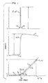
- FIG. 1 there are illustrated plots of laser luminosity L as a function of laser current I (L - I curve), the first derivative of the L - I curve (dL/dI), and the second derivative of the L - I curve (d2L/dI2).
- the basic parameters of a laser are illustrated on the L - I curve and include I th , the threshold current; ⁇ 1, the slope of the L - I curve below I th ; and ⁇ 2, the slope of the L- I curve above I th .
- Also shown on the L - I curve are typical operating points I0,L0 and I1,L1, where I1 is I0 + I M , being the amplitude modulation current signal.
- the d2L/dI2 curve is characterized by a distinct peak (P of FIG. 1) marking the location of threshold current (I th ) and (for some lasers) sharp transitions on either side of the peak such that the curve falls to near-zero levels both above and below threshold.
- the d2L/dI2 peak P represents a readily detectable characteristic which identifies the location of threshold I th and can be used for controlling laser biasing.
- the only characteristic of d2L/dI2 that will vary significantly with parameter variations is the magnitude of the peak P at threshold (I th ). Specifically, P will decrease as temperature increases.
- the magnitude of the detected d2L/dI2 peak is increased by the electronic gain of the feedback circuit.
- the measured peak can be adjusted to a readily detectable value by increasing the electronic gain of the feedback loop.
- the peak P of d2L/dI2 is a readily detectable and stable characteristic which can be utilized as a reference to establish the I0 bias point of the laser.
- An electronic algorithm is utilized to accurately measure the d2L/dI2 characteristic in a time which is short compared to the necessary response time of the feedback loop.
- the algorithm can be implemented inexpensively in integrated circuit form.
- the algorithm is used to generate derivatives of voltage across a laser with respect to the laser bias current (e.g., d2V/dI2).
- the d2V/dI2 curve has a null or notch (A,B) at the threshold current (I th ) and another null or dip in the curve (D) at lower bias currents.
- the existence of two nulls makes detection of the threshold current I th more difficult. Consequently, the Swartz patent states (column 8, lines 53-57) that a simple feedback scheme typically cannot use only d2V/dI2 to optimally determine the bias point of a laser.
- the present invention recognizes that the second derivative of the light output of a laser with respect to the laser bias current (i.e., d2L/dI2) has only one distinct peak at the threshold current (I th ) and as such could be used to control an operating characteristic of a laser (i.e., bias threshold I0 peak light output L, or modulation level).
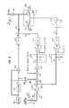
- the dual loop laser stabilization circuit of FIG. 2 has means for determining d2L/dI2 which is used to control the bias current I0 in accordance with the present invention.
- the d2L/dI2 determining means includes, illustratively, clock 200, divider 201, summer 202, transconductance circuit 203, inductor 204, laser 205, photodetector 206, low pass filter 220, transimpedance amplifier 207, exclusive-or circuit 208, multiplier circuit 209 and low pass filter 215.
- the d2L/dI2 signal is generated and used by a control circuit (e.g., 215, 216, 217, 218, 219) as part of a feedback loop to control the bias current I0 of the laser.
- the d2L/dI2 bias current loop includes test current I t generator components 200-203, inductor 204, laser 205, photodetector 206, low pass filter 220, amplifier 207, and bias current control circuit 208,209,215-219.
- a second feedback loop uses the average output power of laser 205 to set and control the laser modulation current I M .
- the second feedback loop includes, illustratively, laser 205, photodetector 206, low pass filter 220, amplifier 207 and modulation current control circuit 210 - 214.
- the d2L/dI2 characteristic is used to control the bias current I0 (see FIG. 1), and an average power loop is used to control modulation current I M .
- the reference voltages V1 and V3 (of FIG. 2) set bias current I0.
- the I0 steady state current is proportional to the difference between reference voltages V1 and V3 (i.e., V3-V1).
- the laser 205 can be biased either below or above threshold I th by setting the gain of amplifier 218 and the reference voltage V3.
- the bias current I0 starts initially at zero and increases to value I01 just below the d2L/dI2 peak as is shown on FIG. 1.
- the gain of amplifier 218 is set at plus one, reference voltage V3 is set to zero and reference voltage V1 is less than zero.
- the above-threshold bias mode is established by inverting the gain of the amplifier 218 and setting V3 greater than zero.
- the bias current at power-on starts at a current greater than I th , and decreases until d2L/dI2 peaks near I02.
- bias current I0 can be set to stabilize at either I01 or I02, the laser bias stabilizing circuit of FIG. 2 can be optimized, respectively, for bandwidth (I02) or extinction ratio (I01).
- reference voltage V1 could be followed by another low pass filter 215 circuit and combined with reference voltage V3 as the positive input to comparator 216.
- the modulation current I M increases until the desired average operating power of the laser 205 is reached.
- the average laser operating power is set using voltage V2 of comparator 211 which controls the modulation current I M .
- a test current (I t ) is generated using circuits 200 - 203.
- An oscillator or clock 200 is used to provide a clock signal at frequency f1 of 50% duty cycle.
- a digital divider circuit 201 divides clock signal f1 to generate signal f2.
- a separate oscillator could also be used to generate f2.
- test current I t is injected into laser 205 via inductor 204.
- the inductor by convention serves to isolate the low frequency transconductance amplifiers 203 and 217 from the high frequency modulator 214. In optimally designed configurations, it may be omitted.
- the light output from laser 205 is coupled to monitoring photodetector 206.
- Photodetector 206 monitors light from laser 205 and outputs a current I p proportional to the instantaneous optical output power of laser 205.
- Low pass filter 220 filters out the high frequency data modulation signal to prevent the saturation of amplifier 207.
- the filtered output current I p of photodetector 206 is used in both a first (average power) and a second (d2L/dI2), i.e., dual, feedback loops.
- Transimpedance amplifier 207 converts the filtered photocurrent I p from photodetector 206 to a voltage V p .
- a partial product ⁇ N is produced from digital signals f1 and f2 using exclusive-or circuit 208.
- a double-balanced mixer or multiplier 209 is used to analog multiply ⁇ N by a voltage V p proportional to the detected photocurrent I p .
- the output of mixer 209 is summed with reference voltage V1 using summing circuit 219.
- the procedure just described involving circuits 200 - 209,215,218-220 generates the second derivative d2L/dI2 signal as the output of low pass filter 215.
- Filter 215 also establishes a dominant pole in the signal path that serves to stabilize the feedback control loop.
- the second derivative d2L/dI2 signal is compared with reference signal V3 using comparator 216.
- the feedback loop adjusts the bias current I0 to the laser so that the detected value of d2L/dI2 corresponds to a bias either just below (I01) or just above (I02) threshold.
- the selection of I01 or I02 is controlled by the polarity of the electronic gain of buffer amplifier 218, and by the reference voltage V3, thus determining the value of bias current when power is first applied to the circuit.
- Circuitry is provided to prevent interference between the dual feedback loops.
- power is applied to the d2L/dI2 loop, while circuit 213 keeps the (average power) modulation current I M loop disabled.
- the average power feedback loop adjusts I M (see FIG. 1) until the proper average power is obtained. Meanwhile, the d2L/dI2 loop maintains dc bias I0 at threshold.
- the operation of the above-described average power feedback loop adjusts the modulation current I M of laser 205, resulting in an optimum modulation current I M setting with variations in laser temperature, data signals, etc.
- the second feedback loop measures the average value of the photocurrent I p .
- Filter 210 removes the low frequency test signal proportional to I t , and also assures the stability of the average power feedback loop.
- the output of filter 210 is proportional to the average power of laser 205.
- Comparator 211 compares filtered voltage V p with reference V2, and the output of 211 is converted to a current I M by transconductance circuit 212.
- Reference signal V2 is duty-cycle compensated so that its dc level changes in proportion to the duty cycle of the data signal 230.
- the voltage reference V2 is used to establish the modulation current I M at a value corresponding to a peak output light level of L1 as shown in FIG. 1.
- the laser current is I0 for a logic ZERO data signal and I0 + I M for a logic ONE data signal.
- the analog and digital circuits of the present invention can be implemented using well-known discrete or integrated circuits using silicon bipolar technology or FET technology, as well as non-silicon technologies (for example, gallium arsenide FET or bipolar).
Landscapes
- Physics & Mathematics (AREA)
- Condensed Matter Physics & Semiconductors (AREA)
- General Physics & Mathematics (AREA)
- Electromagnetism (AREA)
- Optics & Photonics (AREA)
- Semiconductor Lasers (AREA)
Applications Claiming Priority (2)
| Application Number | Priority Date | Filing Date | Title |
|---|---|---|---|
| US291899 | 1988-12-29 | ||
| US07/291,899 US5027362A (en) | 1988-12-29 | 1988-12-29 | Laser control method and circuitry |
Publications (3)
| Publication Number | Publication Date |
|---|---|
| EP0376555A2 true EP0376555A2 (fr) | 1990-07-04 |
| EP0376555A3 EP0376555A3 (fr) | 1991-01-30 |
| EP0376555B1 EP0376555B1 (fr) | 1994-09-21 |
Family
ID=23122351
Family Applications (1)
| Application Number | Title | Priority Date | Filing Date |
|---|---|---|---|
| EP89313101A Expired - Lifetime EP0376555B1 (fr) | 1988-12-29 | 1989-12-14 | Méthode et circuits de réglage d'un laser |
Country Status (4)
| Country | Link |
|---|---|
| US (1) | US5027362A (fr) |
| EP (1) | EP0376555B1 (fr) |
| JP (1) | JPH07109917B2 (fr) |
| DE (1) | DE68918425T2 (fr) |
Cited By (3)
| Publication number | Priority date | Publication date | Assignee | Title |
|---|---|---|---|---|
| EP0580568A3 (fr) * | 1992-07-21 | 1994-04-20 | Alcatel Austria Ag | |
| US6198497B1 (en) | 1998-06-03 | 2001-03-06 | Hewlett-Packard | Adjustment of a laser diode output power compensator |
| EP1139586A3 (fr) * | 2000-03-31 | 2004-09-15 | Avanex Corporation | Circuit de commande d'un laser ultra-linéaire |
Families Citing this family (16)
| Publication number | Priority date | Publication date | Assignee | Title |
|---|---|---|---|---|
| JP3226624B2 (ja) * | 1992-09-24 | 2001-11-05 | 日本オプネクスト株式会社 | レーザダイオード駆動回路及び光伝送装置 |
| US5502298A (en) * | 1992-12-21 | 1996-03-26 | Ericsson Raynet | Apparatus and method for controlling an extinction ratio of a laser diode over temperature |
| US5442510A (en) * | 1993-06-23 | 1995-08-15 | The United States Of America As Represented By The Secretary Of The Navy | Control system for tracking nonlinear systems |
| DE69517614T2 (de) * | 1994-03-22 | 2001-02-15 | Uniphase Opto Holdings Inc., San Jose | Halbleiterdiodenlaser und dessen Herstellungsverfahren |
| US5535038A (en) * | 1994-06-17 | 1996-07-09 | Hinch; Stephen W. | Apparatus and method for determining extinction ratio of digital laser transmitters |
| US5767995A (en) * | 1996-03-13 | 1998-06-16 | Lucent Technologies Inc. | System and methods for assessing the suitability of analog lasers for broadband access applications |
| US6917639B2 (en) * | 2001-08-09 | 2005-07-12 | Ricoh Company, Ltd. | Laser driver circuit |
| US7215891B1 (en) | 2003-06-06 | 2007-05-08 | Jds Uniphase Corporation | Integrated driving, receiving, controlling, and monitoring for optical transceivers |
| US7468998B2 (en) * | 2005-03-25 | 2008-12-23 | Pavilion Integration Corporation | Radio frequency modulation of variable degree and automatic power control using external photodiode sensor for low-noise lasers of various wavelengths |
| JP2007281294A (ja) * | 2006-04-10 | 2007-10-25 | Hitachi Cable Ltd | レーザ制御装置 |
| US7447395B2 (en) * | 2006-06-15 | 2008-11-04 | Sioptical, Inc. | Silicon modulator offset tuning arrangement |
| US7697793B2 (en) * | 2006-06-15 | 2010-04-13 | Lightwire, Inc. | Silicon modulator offset tuning arrangement |
| US7403215B2 (en) * | 2006-08-22 | 2008-07-22 | Lexmark International, Inc. | Current driver and power control for electrophotographic devices |
| US7643525B2 (en) | 2007-10-31 | 2010-01-05 | Lexmark International, Inc. | Current driver and power control for electrophotographic devices |
| JP6032601B2 (ja) * | 2011-12-21 | 2016-11-30 | 住友電工デバイス・イノベーション株式会社 | 半導体光増幅器の制御方法及び測定方法、並びに半導体光増幅装置 |
| EP3002891A4 (fr) * | 2013-06-29 | 2016-04-13 | Huawei Tech Co Ltd | Procédé de contrôle de signaux optiques, dispositif de contrôle de signaux et système de réseau optique |
Family Cites Families (8)
| Publication number | Priority date | Publication date | Assignee | Title |
|---|---|---|---|---|
| USRE31969E (en) * | 1976-03-22 | 1985-08-13 | At&T Bell Laboratories | Laser control circuit |
| US4009385A (en) * | 1976-03-22 | 1977-02-22 | Bell Telephone Laboratories, Incorporated | Laser control circuit |
| US4344173A (en) * | 1978-09-25 | 1982-08-10 | Northern Telecom Limited | Stabilization circuit for a digitally operated laser |
| CA1210070A (fr) * | 1984-10-26 | 1986-08-19 | Northern Telecom Limited | Emetteur laser |
| US4698817A (en) * | 1985-02-28 | 1987-10-06 | Northern Telecom Limited | Peak optical power control circuit for laser driver |
| US4680810A (en) * | 1985-06-28 | 1987-07-14 | American Telephone And Telegraph Company, At&T Bell Labs | Means for controlling a semiconductor device and communication system comprising the means |
| US4868836A (en) * | 1986-02-27 | 1989-09-19 | Spectra-Physics, Inc. | Laser diode power control and modulator circuit |
| DE3706572A1 (de) * | 1987-02-28 | 1988-09-08 | Philips Patentverwaltung | Regelung von laserdioden |
-
1988
- 1988-12-29 US US07/291,899 patent/US5027362A/en not_active Expired - Lifetime
-
1989
- 1989-12-14 EP EP89313101A patent/EP0376555B1/fr not_active Expired - Lifetime
- 1989-12-14 DE DE68918425T patent/DE68918425T2/de not_active Expired - Fee Related
- 1989-12-28 JP JP1345132A patent/JPH07109917B2/ja not_active Expired - Lifetime
Cited By (4)
| Publication number | Priority date | Publication date | Assignee | Title |
|---|---|---|---|---|
| EP0580568A3 (fr) * | 1992-07-21 | 1994-04-20 | Alcatel Austria Ag | |
| US6198497B1 (en) | 1998-06-03 | 2001-03-06 | Hewlett-Packard | Adjustment of a laser diode output power compensator |
| EP0963016A3 (fr) * | 1998-06-03 | 2003-08-13 | Hewlett-Packard Company, A Delaware Corporation | Réglage d'un compensateur de puissance d'un laser à diode |
| EP1139586A3 (fr) * | 2000-03-31 | 2004-09-15 | Avanex Corporation | Circuit de commande d'un laser ultra-linéaire |
Also Published As
| Publication number | Publication date |
|---|---|
| JPH02228085A (ja) | 1990-09-11 |
| US5027362A (en) | 1991-06-25 |
| DE68918425T2 (de) | 1995-01-19 |
| DE68918425D1 (de) | 1994-10-27 |
| EP0376555B1 (fr) | 1994-09-21 |
| JPH07109917B2 (ja) | 1995-11-22 |
| EP0376555A3 (fr) | 1991-01-30 |
Similar Documents
| Publication | Publication Date | Title |
|---|---|---|
| EP0376555B1 (fr) | Méthode et circuits de réglage d'un laser | |
| EP0513002B1 (fr) | Circuit de commande de laser | |
| US4796266A (en) | Laser driver circuit with dynamic bias | |
| US4237427A (en) | Apparatus for stabilizing a laser | |
| US5311005A (en) | Optical transmitters | |
| GB2025121A (en) | Improvements in or relating to the stabilisation of injection lasers | |
| AU593889B2 (en) | Method and apparatus for controlling power output of a laser | |
| GB1563944A (en) | Imjection lasers | |
| US4101847A (en) | Laser control circuit | |
| US4626676A (en) | Light detector having a photodiode with bias control | |
| US5309269A (en) | Light transmitter | |
| US4924470A (en) | Laser diode control apparatus | |
| US7492797B2 (en) | Laser driver circuit | |
| US6370170B1 (en) | Laser frequency stabilization apparatus | |
| US7782916B2 (en) | Laser diode driver able to precisely control the driving current | |
| JP2002033548A (ja) | モード同期半導体レーザの駆動方法及び装置 | |
| JP3264669B2 (ja) | レーザ制御法とその装置 | |
| US20030067947A1 (en) | Laser control circuit for maintaining constant power and extinction ratio | |
| CA1133591A (fr) | Methode et dispositif d'ttaque pour dispositifs a seuil non lineraires | |
| JP2005057216A (ja) | レーザダイオード駆動回路及び光送信装置 | |
| JPS6190487A (ja) | 半導体レ−ザ駆動回路 | |
| US6744313B2 (en) | Power amplifier driver and method of using | |
| JPS6091687A (ja) | 半導体レ−ザの出力安定化方式 | |
| EP1239603B1 (fr) | Circuit d'excitation d'un amplificateur de puissance et procédé d'utilisation | |
| JPS5941315B2 (ja) | 半導体レ−ザの出力安定化方式 |
Legal Events
| Date | Code | Title | Description |
|---|---|---|---|
| PUAI | Public reference made under article 153(3) epc to a published international application that has entered the european phase |
Free format text: ORIGINAL CODE: 0009012 |
|
| AK | Designated contracting states |
Kind code of ref document: A2 Designated state(s): DE |
|
| PUAL | Search report despatched |
Free format text: ORIGINAL CODE: 0009013 |
|
| AK | Designated contracting states |
Kind code of ref document: A3 Designated state(s): DE |
|
| 17P | Request for examination filed |
Effective date: 19910712 |
|
| 17Q | First examination report despatched |
Effective date: 19921221 |
|
| RAP3 | Party data changed (applicant data changed or rights of an application transferred) |
Owner name: AT&T CORP. |
|
| GRAA | (expected) grant |
Free format text: ORIGINAL CODE: 0009210 |
|
| AK | Designated contracting states |
Kind code of ref document: B1 Designated state(s): DE |
|
| REF | Corresponds to: |
Ref document number: 68918425 Country of ref document: DE Date of ref document: 19941027 |
|
| PLBE | No opposition filed within time limit |
Free format text: ORIGINAL CODE: 0009261 |
|
| STAA | Information on the status of an ep patent application or granted ep patent |
Free format text: STATUS: NO OPPOSITION FILED WITHIN TIME LIMIT |
|
| 26N | No opposition filed | ||
| PGFP | Annual fee paid to national office [announced via postgrant information from national office to epo] |
Ref country code: DE Payment date: 20011230 Year of fee payment: 13 |
|
| PG25 | Lapsed in a contracting state [announced via postgrant information from national office to epo] |
Ref country code: DE Free format text: LAPSE BECAUSE OF NON-PAYMENT OF DUE FEES Effective date: 20030701 |