EP0376830B1 - Procédé de réalisation d'un écran plat à matrice active et d'une RAM, utilisant des composants MIM - Google Patents
Procédé de réalisation d'un écran plat à matrice active et d'une RAM, utilisant des composants MIM Download PDFInfo
- Publication number
- EP0376830B1 EP0376830B1 EP89403632A EP89403632A EP0376830B1 EP 0376830 B1 EP0376830 B1 EP 0376830B1 EP 89403632 A EP89403632 A EP 89403632A EP 89403632 A EP89403632 A EP 89403632A EP 0376830 B1 EP0376830 B1 EP 0376830B1
- Authority
- EP
- European Patent Office
- Prior art keywords
- film
- temperature
- matrix
- addressing
- mim
- Prior art date
- Legal status (The legal status is an assumption and is not a legal conclusion. Google has not performed a legal analysis and makes no representation as to the accuracy of the status listed.)
- Expired - Lifetime
Links
Images


Classifications
-
- H—ELECTRICITY
- H10—SEMICONDUCTOR DEVICES; ELECTRIC SOLID-STATE DEVICES NOT OTHERWISE PROVIDED FOR
- H10B—ELECTRONIC MEMORY DEVICES
- H10B12/00—Dynamic random access memory [DRAM] devices
- H10B12/30—DRAM devices comprising one-transistor - one-capacitor [1T-1C] memory cells
-
- H—ELECTRICITY
- H10—SEMICONDUCTOR DEVICES; ELECTRIC SOLID-STATE DEVICES NOT OTHERWISE PROVIDED FOR
- H10D—INORGANIC ELECTRIC SEMICONDUCTOR DEVICES
- H10D86/00—Integrated devices formed in or on insulating or conducting substrates, e.g. formed in silicon-on-insulator [SOI] substrates or on stainless steel or glass substrates
-
- H—ELECTRICITY
- H10—SEMICONDUCTOR DEVICES; ELECTRIC SOLID-STATE DEVICES NOT OTHERWISE PROVIDED FOR
- H10N—ELECTRIC SOLID-STATE DEVICES NOT OTHERWISE PROVIDED FOR
- H10N70/00—Solid-state devices having no potential barriers, and specially adapted for rectifying, amplifying, oscillating or switching
Definitions
- the present invention relates to a method for producing a flat screen with active matrix and a RAM, using MIM components.
- the invention finds applications in particular in display, in the production of liquid crystal flat screens of the active matrix type and in data processing, in the production of dynamic RAM memories (direct access memory).
- a large number of types of liquid crystal display screens are known.
- the one which comes closest to the screen which the present invention envisages manufacturing is the so-called active matrix type.
- An advantageous production method is the two-level masking method disclosed in document FR-A-2 533 072. This method makes it possible to associate a thin film transistor (TFT for "Thin Film Transistor") with each pixel. grid is connected to an address line, the source to a column and the drain to the pixel electrode.
- TFT Thin Film Transistor
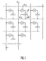
- FIG. 1 The general diagram of such a device is represented in FIG. 1.
- the general diagram of such a device is represented in FIG. 1.
- the second armatures or counter-electrodes cel are connected to address lines Li carried by a second plate, not shown.
- Document GB-A-2 091 468 discloses such a screen and a production method in the case where the non-linear element Sij is a so-called MIM component, that is to say a metal-insulator-metal stack.
- the MIM components are obtained by deposition of a first metallic film, anodization producing an oxide film, then deposition of a second metallic film on the oxide.
- the object of the invention is to remedy all these drawbacks. To this end, it proposes a particularly simple method for producing MIM components and which, when used to produce a display screen, requires only two masking levels. The process overcomes all the difficulties associated with anodization and leads to a conduction phenomenon almost insensitive to temperature and brightness.
- one proceeds by mutual redox of two materials brought into contact with one another.
- the formation of a thin layer of oxide between an oxidizing conductor and an oxidizable conductor by increasing the temperature is not a new physical phenomenon in itself. It is mentioned for example in the article by AKIO MIMURA et al. cited above. However, it is essential to emphasize that this phenomenon has never been implemented to form an active matrix display screen with MIM components. In the article cited, if the phenomenon in question is mentioned, it is to emphasize its defective nature and it is well recommended to avoid it.
- the target structure is not MIM but TFT. An ohmic contact must be formed on the n-doped silicon source of the TFT and this contact is obtained by depositing ITO.
- the invention has yet another advantage linked to the screen control time.
- the oxidizable conductor was a semiconductor, such as silicon for example
- the formation of an oxide layer was accompanied by the appearance of a space charge zone at the semiconductor-insulator interface.
- This space charge has the effect of creating a second capacitor in series with the capacitor corresponding to the insulating layer, which results in a considerable reduction in the capacity of the assembly, compared to the value that would be obtained for example if the oxidizable conductor was made of metal.
- the capacity of the MIM component must normally be lower than the pixel capacity, if we want the charges defining the electric field controlling the display to be present above all on the pixel.
- the capacity of the MIM component has been around a third of the capacity of a pixel.
- the presence of the space charge decreases the capacity of the MIM component to a value equal to approximately one tenth of the capacity of the pixel, which is much more favorable. It is therefore the pixel that will make the largest capacitive contribution to the display screen.
- the invention recommends the use of a semiconductor as an oxidizable conductive material.
- This semiconductor can be silicon, germanium, a binary compound such as gallium arsenide or indium phosphide, or a ternary (GaAlAs) or even quaternary compound.
- the oxidizing conductive material it can be taken from the group of conductive metallic oxides of the indium oxide (In2O3), tin oxide (SnO2), indium tin oxide (ITO), (In2O3 + SnO2 ), zinc oxide (ZnO), etc.
- the oxidizable conductive material when it is not semiconductor, can be taken from the group of mixtures of oxides (V2O5 - P2O5) (V2O5 - PbO - Fe2O3), metals Al, Ti, Ta, Ag, Cr, Cu, Mn, Mo, etc., or oxidizable alloys.
- the oxide formation temperature is greater than 200 ° C and in general less than 700 ° C. It is therefore a low or medium temperature technology.
- the temperature is advantageously around 350 ° C.
- the temperature can be approximately 625 ° C.
- the temperature can be approximately 520 ° C.
- the thermal step can be carried out under vacuum or in the presence of gas (argon, oxygen for example). Its duration depends on the thickness of the desired insulating layer. In general, this duration is of the order of 3 hours.
- the thermal step can be carried out after formation of the stack, but it can also take place during the formation of this stack if the layer deposition operation is carried out in the range required for the redox.
- the substrate is made of glass
- the oxidizing conductive material is ITO (tin and indium oxide)
- the oxidizable material is silicon, doped or not.
- the insulating layer of the MIM components is then silica resulting from the oxidation of silicon by the ITO layer.
- FIGS. 2A and 2B we see different stages in the production of the plate which supports the pixel matrix and the MIMs, according to a first embodiment employing an oxidizing layer situated below and an oxidizable silicon layer situated above. It will be observed, in this regard, that this provision is the reverse of that of the document cited above, for the reasons already cited.
- step 2Ad is then a step of aging and homogenization of MIM structures.
- the order of the materials is reversed and the oxidizable conductor is then deposited, then the oxidizing conductor. That's what is illustrated in FIGS. 3A and 3B in the case where the oxidizing material is ITO and the oxidizable material is tantalum.
- the steps and operations are as follows:
- FIG. 2A, 2B, 3A, 3B These operations make it possible to constitute the support plate for the electrode matrix and for the row of addressing columns. It remains to realize the counter plate with the counter electrodes and the addressing lines.
- This counter-plate can be produced by any known means, as illustrated in FIG. 4, by depositing on a glass plate a layer of ITO then etching to obtain lines 70 and counter-electrodes 72.
- the invention is not limited to the production of display screens. It also applies to the production of components such as dynamic RAM memories.
- FIGS. 5A and 5B illustrate an exemplary embodiment of such a memory.
- Such a device is structurally comparable to the device of FIG. 1, except that the addressing lines and columns are contained in or on the same semiconductor substrate. The operations can therefore be substantially the same as those described above, except that the various layers no longer have to be transparent.
- the MIM switches 94 and capacitors 96 created automatically and that, on the other hand, the capacitors 96 formed above the doped silicon, having a very thin insulating layer or a significant value, reduce the surface and therefore increase the integration density.
Landscapes
- Liquid Crystal (AREA)
- Glass Compositions (AREA)
- Electrochromic Elements, Electrophoresis, Or Variable Reflection Or Absorption Elements (AREA)
- Nitrogen And Oxygen Or Sulfur-Condensed Heterocyclic Ring Systems (AREA)
- Steroid Compounds (AREA)
- Devices For Indicating Variable Information By Combining Individual Elements (AREA)
- Semiconductor Memories (AREA)
Applications Claiming Priority (2)
| Application Number | Priority Date | Filing Date | Title |
|---|---|---|---|
| FR8817246A FR2641645B1 (fr) | 1988-12-27 | 1988-12-27 | Procede de realisation d'un composant mim et application a la realisation d'un ecran plat ou d'une ram |
| FR8817246 | 1988-12-27 |
Publications (2)
| Publication Number | Publication Date |
|---|---|
| EP0376830A1 EP0376830A1 (fr) | 1990-07-04 |
| EP0376830B1 true EP0376830B1 (fr) | 1994-08-10 |
Family
ID=9373472
Family Applications (1)
| Application Number | Title | Priority Date | Filing Date |
|---|---|---|---|
| EP89403632A Expired - Lifetime EP0376830B1 (fr) | 1988-12-27 | 1989-12-22 | Procédé de réalisation d'un écran plat à matrice active et d'une RAM, utilisant des composants MIM |
Country Status (9)
| Country | Link |
|---|---|
| US (1) | US5086009A (ja) |
| EP (1) | EP0376830B1 (ja) |
| JP (1) | JPH02226231A (ja) |
| AT (1) | ATE109925T1 (ja) |
| CA (1) | CA2006465A1 (ja) |
| DE (1) | DE68917450T2 (ja) |
| FI (1) | FI896139A7 (ja) |
| FR (1) | FR2641645B1 (ja) |
| IL (1) | IL92771A0 (ja) |
Families Citing this family (7)
| Publication number | Priority date | Publication date | Assignee | Title |
|---|---|---|---|---|
| GB9117680D0 (en) * | 1991-08-16 | 1991-10-02 | Philips Electronic Associated | Electronic matrix array devices |
| US5422293A (en) * | 1991-12-24 | 1995-06-06 | Casio Computer Co., Ltd. | Method for manufacturing a TFT panel |
| KR950008931B1 (ko) * | 1992-07-22 | 1995-08-09 | 삼성전자주식회사 | 표시패널의 제조방법 |
| JP3302187B2 (ja) * | 1994-08-18 | 2002-07-15 | キヤノン株式会社 | 薄膜トランジスタ、これを用いた半導体装置、液晶表示装置 |
| US6040201A (en) * | 1996-09-17 | 2000-03-21 | Citizen Watch Co., Ltd. | Method of manufacturing thin film diode |
| JP4497601B2 (ja) * | 1999-11-01 | 2010-07-07 | シャープ株式会社 | 液晶表示装置の製造方法 |
| US7737357B2 (en) * | 2006-05-04 | 2010-06-15 | Sunpower Corporation | Solar cell having doped semiconductor heterojunction contacts |
Family Cites Families (10)
| Publication number | Priority date | Publication date | Assignee | Title |
|---|---|---|---|---|
| US4838656A (en) * | 1980-10-06 | 1989-06-13 | Andus Corporation | Transparent electrode fabrication |
| FR2505070B1 (fr) * | 1981-01-16 | 1986-04-04 | Suwa Seikosha Kk | Dispositif non lineaire pour un panneau d'affichage a cristaux liquides et procede de fabrication d'un tel panneau d'affichage |
| AT371388B (de) * | 1981-10-09 | 1983-06-27 | Voest Alpine Ag | Plattenkokille zum stranggiessen |
| JPS60149025A (ja) * | 1984-01-13 | 1985-08-06 | Seiko Epson Corp | 液晶表示装置 |
| JPH0627980B2 (ja) * | 1984-10-17 | 1994-04-13 | レタ・フランセ・ルプレザント・パ・ル・ミニストル・デ・ペ・テ・テ・(セントル・ナシヨナル・デチユ−ド・デ・テレコミユニカシオン) | 能動マトリクスデイスプレイスクリ−ンの製造方法 |
| US4828370A (en) * | 1985-10-04 | 1989-05-09 | Seiko Instruments & Electronics Ltd. | Switching element with nonlinear resistive, nonstoichiometric material |
| JPH0754388B2 (ja) * | 1986-08-04 | 1995-06-07 | 株式会社リコー | Mimアクテイブマトリツクス液晶表示素子 |
| US4907040A (en) * | 1986-09-17 | 1990-03-06 | Konishiroku Photo Industry Co., Ltd. | Thin film Schottky barrier device |
| JP2816549B2 (ja) * | 1986-10-22 | 1998-10-27 | セイコーインスツルメンツ株式会社 | 電気光学装置 |
| JP2695635B2 (ja) * | 1987-04-10 | 1998-01-14 | シチズン時計株式会社 | 液晶表示装置 |
-
1988
- 1988-12-27 FR FR8817246A patent/FR2641645B1/fr not_active Expired - Fee Related
-
1989
- 1989-12-18 IL IL92771A patent/IL92771A0/xx not_active IP Right Cessation
- 1989-12-20 FI FI896139A patent/FI896139A7/fi not_active IP Right Cessation
- 1989-12-21 US US07/454,758 patent/US5086009A/en not_active Expired - Fee Related
- 1989-12-21 CA CA002006465A patent/CA2006465A1/en not_active Abandoned
- 1989-12-22 DE DE68917450T patent/DE68917450T2/de not_active Expired - Fee Related
- 1989-12-22 EP EP89403632A patent/EP0376830B1/fr not_active Expired - Lifetime
- 1989-12-22 AT AT89403632T patent/ATE109925T1/de not_active IP Right Cessation
- 1989-12-27 JP JP1336829A patent/JPH02226231A/ja active Pending
Also Published As
| Publication number | Publication date |
|---|---|
| ATE109925T1 (de) | 1994-08-15 |
| FI896139A0 (fi) | 1989-12-20 |
| US5086009A (en) | 1992-02-04 |
| DE68917450D1 (de) | 1994-09-15 |
| IL92771A0 (en) | 1990-09-17 |
| FI896139A7 (fi) | 1990-06-28 |
| FR2641645A1 (fr) | 1990-07-13 |
| CA2006465A1 (en) | 1990-06-27 |
| FR2641645B1 (fr) | 1991-04-26 |
| JPH02226231A (ja) | 1990-09-07 |
| DE68917450T2 (de) | 1995-03-30 |
| EP0376830A1 (fr) | 1990-07-04 |
Similar Documents
| Publication | Publication Date | Title |
|---|---|---|
| EP0216673B1 (fr) | Procédé de fabrication d'un transistor de commande pour écran plat de visualisation, et élément de commande réalisé selon ce procédé | |
| US7528401B2 (en) | Agglomeration elimination for metal sputter deposition of chalcogenides | |
| EP0198754B1 (fr) | Procédé de réalisation de matrices de commande à diodes pour écran plat de visualisation électrooptique, et écran plat réalisé par ce procédé | |
| EP0200599B1 (fr) | Procédé de réalisation d'éléments de commande non linéaire pour écran plat de visualisation électrooptique et écran plat réalisé selon ce procédé | |
| FR2488013A1 (fr) | Dispositif a matrice d'elements actifs | |
| WO1988002872A1 (fr) | Ecran de visualisation electro-optique a transistors de commande et procede de realisation | |
| WO2010012683A1 (fr) | Dispositif memoire et memoire cbram a fiabilite amelioree | |
| EP0214033B1 (fr) | Procédé de fabrication d'un détecteur d'image lumineuse, et détecteur linéaire d'images obtenu par ce procédé | |
| EP0246945B1 (fr) | Ecran de visualisation électrooptique, et procédé de réalisation | |
| EP0376830B1 (fr) | Procédé de réalisation d'un écran plat à matrice active et d'une RAM, utilisant des composants MIM | |
| EP0202150B1 (fr) | Elément de commande non linéaire pour écran plat de visualisation électrooptique et son procédé de fabrication | |
| EP0506528B1 (fr) | Structure de commande matricielle pour écran de visualisation | |
| WO1994021102A2 (fr) | Procede de fabrication de transistors a couches minces etages directs | |
| EP0558418A1 (fr) | Cellule mémoire non volatile du type métal-ferroélectrique semi-conducteur | |
| FR3104813A1 (fr) | Cellule elementaire comportant une memoire resistive et un dispositif destine a former un selecteur, matrice de cellules, procedes de fabrication et d’initialisation associes | |
| EP0485285A1 (fr) | Dispositif électrooptique bistable, écran comportant un tel dispositif et procédé de mise en oeuvre de cet écran | |
| EP3840049A1 (fr) | Cellule elementaire comportant une memoire resistive et procede d'initialisation associe | |
| FR3066310A1 (fr) | Cellule memoire de type ram resistive | |
| EP0188946B1 (fr) | Elément capacitif intégré sur une pastille de circuit intégré, et procédé de réalisation de cet élément actif | |
| EP0266252B1 (fr) | Ecran de visualisation électrooptique à transistors de commande et procédé de réalisation | |
| WO2007085554A2 (fr) | Matrice active d'affichage a diodes electroluminescentes | |
| FR2532116A1 (fr) | Transistor a couche mince et dispositif d'affichage a cristaux liquides utilisant ce transistor | |
| FR3132386A1 (fr) | Transistor non-volatil à effet de champ à base de gaz bidimensionnel d’électrons | |
| FR3150036A1 (fr) | Circuit mémoire comprenant des cellules électroniques et un circuit de contrôle | |
| JP3341346B2 (ja) | 非線形素子の製造方法 |
Legal Events
| Date | Code | Title | Description |
|---|---|---|---|
| PUAI | Public reference made under article 153(3) epc to a published international application that has entered the european phase |
Free format text: ORIGINAL CODE: 0009012 |
|
| AK | Designated contracting states |
Kind code of ref document: A1 Designated state(s): AT BE CH DE ES FR GB GR IT LI LU NL SE |
|
| 17P | Request for examination filed |
Effective date: 19901208 |
|
| 17Q | First examination report despatched |
Effective date: 19930928 |
|
| GRAA | (expected) grant |
Free format text: ORIGINAL CODE: 0009210 |
|
| AK | Designated contracting states |
Kind code of ref document: B1 Designated state(s): AT BE CH DE ES FR GB GR IT LI LU NL SE |
|
| PG25 | Lapsed in a contracting state [announced via postgrant information from national office to epo] |
Ref country code: IT Free format text: LAPSE BECAUSE OF FAILURE TO SUBMIT A TRANSLATION OF THE DESCRIPTION OR TO PAY THE FEE WITHIN THE PRE;WARNING: LAPSES OF ITALIAN PATENTS WITH EFFECTIVE DATE BEFORE 2007 MAY HAVE OCCURRED AT ANY TIME BEFORE 2007. THE CORRECT EFFECTIVE DATE MAY BE DIFFERENT FROM THE ONE RECORDED.SCRIBED TIME-LIMIT Effective date: 19940810 Ref country code: AT Effective date: 19940810 Ref country code: GR Free format text: LAPSE BECAUSE OF FAILURE TO SUBMIT A TRANSLATION OF THE DESCRIPTION OR TO PAY THE FEE WITHIN THE PRESCRIBED TIME-LIMIT Effective date: 19940810 Ref country code: ES Free format text: THE PATENT HAS BEEN ANNULLED BY A DECISION OF A NATIONAL AUTHORITY Effective date: 19940810 Ref country code: NL Effective date: 19940810 |
|
| REF | Corresponds to: |
Ref document number: 109925 Country of ref document: AT Date of ref document: 19940815 Kind code of ref document: T |
|
| REF | Corresponds to: |
Ref document number: 68917450 Country of ref document: DE Date of ref document: 19940915 |
|
| PG25 | Lapsed in a contracting state [announced via postgrant information from national office to epo] |
Ref country code: SE Effective date: 19941110 |
|
| GBT | Gb: translation of ep patent filed (gb section 77(6)(a)/1977) |
Effective date: 19941114 |
|
| PGFP | Annual fee paid to national office [announced via postgrant information from national office to epo] |
Ref country code: CH Payment date: 19941214 Year of fee payment: 6 |
|
| PGFP | Annual fee paid to national office [announced via postgrant information from national office to epo] |
Ref country code: DE Payment date: 19941215 Year of fee payment: 6 Ref country code: GB Payment date: 19941215 Year of fee payment: 6 |
|
| PGFP | Annual fee paid to national office [announced via postgrant information from national office to epo] |
Ref country code: BE Payment date: 19941220 Year of fee payment: 6 Ref country code: FR Payment date: 19941220 Year of fee payment: 6 |
|
| PG25 | Lapsed in a contracting state [announced via postgrant information from national office to epo] |
Ref country code: LU Free format text: LAPSE BECAUSE OF NON-PAYMENT OF DUE FEES Effective date: 19941231 |
|
| NLV1 | Nl: lapsed or annulled due to failure to fulfill the requirements of art. 29p and 29m of the patents act | ||
| REG | Reference to a national code |
Ref country code: GB Ref legal event code: 732E |
|
| REG | Reference to a national code |
Ref country code: FR Ref legal event code: TP |
|
| PLBE | No opposition filed within time limit |
Free format text: ORIGINAL CODE: 0009261 |
|
| STAA | Information on the status of an ep patent application or granted ep patent |
Free format text: STATUS: NO OPPOSITION FILED WITHIN TIME LIMIT |
|
| 26N | No opposition filed | ||
| PG25 | Lapsed in a contracting state [announced via postgrant information from national office to epo] |
Ref country code: GB Effective date: 19951222 |
|
| PG25 | Lapsed in a contracting state [announced via postgrant information from national office to epo] |
Ref country code: BE Effective date: 19951231 Ref country code: LI Effective date: 19951231 Ref country code: CH Effective date: 19951231 |
|
| BERE | Be: lapsed |
Owner name: CHAMBRE DE COMMERCE ET D'INDUSTRIE DE PARIS CCIP Effective date: 19951231 |
|
| GBPC | Gb: european patent ceased through non-payment of renewal fee |
Effective date: 19951222 |
|
| REG | Reference to a national code |
Ref country code: CH Ref legal event code: PL |
|
| PG25 | Lapsed in a contracting state [announced via postgrant information from national office to epo] |
Ref country code: FR Effective date: 19960830 |
|
| PG25 | Lapsed in a contracting state [announced via postgrant information from national office to epo] |
Ref country code: DE Effective date: 19960903 |
|
| REG | Reference to a national code |
Ref country code: FR Ref legal event code: ST |