EP0379449A1 - Verfahren zur Herstellung von integrierten Schaltungen - Google Patents
Verfahren zur Herstellung von integrierten Schaltungen Download PDFInfo
- Publication number
- EP0379449A1 EP0379449A1 EP90420019A EP90420019A EP0379449A1 EP 0379449 A1 EP0379449 A1 EP 0379449A1 EP 90420019 A EP90420019 A EP 90420019A EP 90420019 A EP90420019 A EP 90420019A EP 0379449 A1 EP0379449 A1 EP 0379449A1
- Authority
- EP
- European Patent Office
- Prior art keywords
- transistors
- polycrystalline silicon
- level
- layer
- insulation layer
- Prior art date
- Legal status (The legal status is an assumption and is not a legal conclusion. Google has not performed a legal analysis and makes no representation as to the accuracy of the status listed.)
- Withdrawn
Links
Images

Classifications
-
- H—ELECTRICITY
- H10—SEMICONDUCTOR DEVICES; ELECTRIC SOLID-STATE DEVICES NOT OTHERWISE PROVIDED FOR
- H10D—INORGANIC ELECTRIC SEMICONDUCTOR DEVICES
- H10D84/00—Integrated devices formed in or on semiconductor substrates that comprise only semiconducting layers, e.g. on Si wafers or on GaAs-on-Si wafers
- H10D84/01—Manufacture or treatment
- H10D84/0123—Integrating together multiple components covered by H10D12/00 or H10D30/00, e.g. integrating multiple IGBTs
- H10D84/0126—Integrating together multiple components covered by H10D12/00 or H10D30/00, e.g. integrating multiple IGBTs the components including insulated gates, e.g. IGFETs
- H10D84/0135—Manufacturing their gate conductors
- H10D84/014—Manufacturing their gate conductors the gate conductors having different materials or different implants
-
- H—ELECTRICITY
- H10—SEMICONDUCTOR DEVICES; ELECTRIC SOLID-STATE DEVICES NOT OTHERWISE PROVIDED FOR
- H10B—ELECTRONIC MEMORY DEVICES
- H10B41/00—Electrically erasable-and-programmable ROM [EEPROM] devices comprising floating gates
- H10B41/40—Electrically erasable-and-programmable ROM [EEPROM] devices comprising floating gates characterised by the peripheral circuit region
-
- H—ELECTRICITY
- H10—SEMICONDUCTOR DEVICES; ELECTRIC SOLID-STATE DEVICES NOT OTHERWISE PROVIDED FOR
- H10B—ELECTRONIC MEMORY DEVICES
- H10B41/00—Electrically erasable-and-programmable ROM [EEPROM] devices comprising floating gates
- H10B41/40—Electrically erasable-and-programmable ROM [EEPROM] devices comprising floating gates characterised by the peripheral circuit region
- H10B41/42—Simultaneous manufacture of periphery and memory cells
- H10B41/49—Simultaneous manufacture of periphery and memory cells comprising different types of peripheral transistor
-
- H—ELECTRICITY
- H10—SEMICONDUCTOR DEVICES; ELECTRIC SOLID-STATE DEVICES NOT OTHERWISE PROVIDED FOR
- H10D—INORGANIC ELECTRIC SEMICONDUCTOR DEVICES
- H10D84/00—Integrated devices formed in or on semiconductor substrates that comprise only semiconducting layers, e.g. on Si wafers or on GaAs-on-Si wafers
- H10D84/01—Manufacture or treatment
- H10D84/0123—Integrating together multiple components covered by H10D12/00 or H10D30/00, e.g. integrating multiple IGBTs
- H10D84/0126—Integrating together multiple components covered by H10D12/00 or H10D30/00, e.g. integrating multiple IGBTs the components including insulated gates, e.g. IGFETs
- H10D84/0144—Manufacturing their gate insulating layers
-
- H—ELECTRICITY
- H10—SEMICONDUCTOR DEVICES; ELECTRIC SOLID-STATE DEVICES NOT OTHERWISE PROVIDED FOR
- H10D—INORGANIC ELECTRIC SEMICONDUCTOR DEVICES
- H10D84/00—Integrated devices formed in or on semiconductor substrates that comprise only semiconducting layers, e.g. on Si wafers or on GaAs-on-Si wafers
- H10D84/01—Manufacture or treatment
- H10D84/02—Manufacture or treatment characterised by using material-based technologies
- H10D84/03—Manufacture or treatment characterised by using material-based technologies using Group IV technology, e.g. silicon technology or silicon-carbide [SiC] technology
- H10D84/038—Manufacture or treatment characterised by using material-based technologies using Group IV technology, e.g. silicon technology or silicon-carbide [SiC] technology using silicon technology, e.g. SiGe
-
- H—ELECTRICITY
- H10—SEMICONDUCTOR DEVICES; ELECTRIC SOLID-STATE DEVICES NOT OTHERWISE PROVIDED FOR
- H10D—INORGANIC ELECTRIC SEMICONDUCTOR DEVICES
- H10D84/00—Integrated devices formed in or on semiconductor substrates that comprise only semiconducting layers, e.g. on Si wafers or on GaAs-on-Si wafers
- H10D84/80—Integrated devices formed in or on semiconductor substrates that comprise only semiconducting layers, e.g. on Si wafers or on GaAs-on-Si wafers characterised by the integration of at least one component covered by groups H10D12/00 or H10D30/00, e.g. integration of IGFETs
- H10D84/82—Integrated devices formed in or on semiconductor substrates that comprise only semiconducting layers, e.g. on Si wafers or on GaAs-on-Si wafers characterised by the integration of at least one component covered by groups H10D12/00 or H10D30/00, e.g. integration of IGFETs of only field-effect components
- H10D84/83—Integrated devices formed in or on semiconductor substrates that comprise only semiconducting layers, e.g. on Si wafers or on GaAs-on-Si wafers characterised by the integration of at least one component covered by groups H10D12/00 or H10D30/00, e.g. integration of IGFETs of only field-effect components of only insulated-gate FETs [IGFET]
- H10D84/83135—Integrated devices formed in or on semiconductor substrates that comprise only semiconducting layers, e.g. on Si wafers or on GaAs-on-Si wafers characterised by the integration of at least one component covered by groups H10D12/00 or H10D30/00, e.g. integration of IGFETs of only field-effect components of only insulated-gate FETs [IGFET] the IGFETs characterised by having different gate conductor materials or different gate conductor implants
-
- H—ELECTRICITY
- H10—SEMICONDUCTOR DEVICES; ELECTRIC SOLID-STATE DEVICES NOT OTHERWISE PROVIDED FOR
- H10D—INORGANIC ELECTRIC SEMICONDUCTOR DEVICES
- H10D84/00—Integrated devices formed in or on semiconductor substrates that comprise only semiconducting layers, e.g. on Si wafers or on GaAs-on-Si wafers
- H10D84/80—Integrated devices formed in or on semiconductor substrates that comprise only semiconducting layers, e.g. on Si wafers or on GaAs-on-Si wafers characterised by the integration of at least one component covered by groups H10D12/00 or H10D30/00, e.g. integration of IGFETs
- H10D84/82—Integrated devices formed in or on semiconductor substrates that comprise only semiconducting layers, e.g. on Si wafers or on GaAs-on-Si wafers characterised by the integration of at least one component covered by groups H10D12/00 or H10D30/00, e.g. integration of IGFETs of only field-effect components
- H10D84/83—Integrated devices formed in or on semiconductor substrates that comprise only semiconducting layers, e.g. on Si wafers or on GaAs-on-Si wafers characterised by the integration of at least one component covered by groups H10D12/00 or H10D30/00, e.g. integration of IGFETs of only field-effect components of only insulated-gate FETs [IGFET]
- H10D84/8314—Integrated devices formed in or on semiconductor substrates that comprise only semiconducting layers, e.g. on Si wafers or on GaAs-on-Si wafers characterised by the integration of at least one component covered by groups H10D12/00 or H10D30/00, e.g. integration of IGFETs of only field-effect components of only insulated-gate FETs [IGFET] the IGFETs characterised by having gate insulating layers with different properties
Definitions
- the present invention relates to the field of manufacturing integrated circuits.
- the present invention aims to provide a method of simultaneously manufacturing floating gate transistors of electrically programmable non-volatile memories (EPROM memories), high voltage transistors and logic transistors, in which the logic transistors and memory transistors have a very short channel length of 500 nm, while the channel length of high voltage transistors is of the order of 800 to 1000 nm.
- EPROM memories electrically programmable non-volatile memories
- the logic transistors and memory transistors have a very short channel length of 500 nm, while the channel length of high voltage transistors is of the order of 800 to 1000 nm.
- the present invention provides for choosing logic transistors comprising a gate oxide thickness less than that of memory transistors and high voltage transistors, the logic transistors supporting a voltage of 3.3 volts.
- the voltage applied to the logic transistors is 5 volts, which has the drawback of accelerated aging of the transistors by trapping hot carriers in the gate oxide when the channel length dimensions drop to 500 nm.
- the reduction of the voltage to 3.3 volts is for example obtained by producing a voltage reducer integrated into the circuit.
- the current between the drain and the source of a MOS transistor is inversely proportional to the thickness of the gate oxide layer.
- the reduction in the thickness of the gate oxide layer of the logic transistors makes it possible to maintain a significant current value and good performance.
- Memory transistors and high voltage transistors support a voltage of, for example, 10 volts.
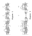
- FIG. 1 represents, in an intermediate manufacturing step, a sectional view of an integrated circuit comprising floating gate transistors of EPROM memory (part I), logic transistors (part II) and high voltage transistors (part III ).
- the devices are produced on a substrate 1.
- Thick oxide zones 2 have been formed between the locations of the transistors.
- a first gate oxide layer 3 Between each thick oxide zone 2, a first gate oxide layer 3.
- a first level of polycrystalline silicon 4 and an insulation layer 5 have been deposited.
- This isolation layer 5 and this first level of polycrystalline silicon 4 have been etched in the memory area to define a band of the bilayer, isolation layer on the first level of polycrystalline silicon.
- An oxide zone 7, called the corner oxide zone has been produced in the memory zone at the level of the visible lateral edges of the first level of polycrystalline silicon 4.
- the thick oxide zones 2 have for example a thickness of 700 nm and the gate oxide layers 3 have for example a thickness of 20 nm.
- the isolation layer 5 is constituted for example by a stack of three levels: Silicon oxide / Silicon nitride / Silicon oxide, designated by ONO.
- FIG. 2 represents the circuit after masking with a photosensitive resin 11 of the memory area and of the location of the high-voltage transistors, and after etching of the insulation layer 5, of the first level of polycrystalline silicon 4 and of the layer d gate oxide 3 at the location of the logic transistors.
- the resin 11 is then removed.
- a second layer of gate oxide 16 was produced (in the memory area and at the location of the high-voltage transistors, this layer of gate oxide 16 merges with layer d isolation 5 and is not shown) and deposited a second level of polycrystalline silicon 17.
- the gate oxide layer 16 has for example a thickness of 12 nm.
- corner oxide zones 7 make it possible to isolate in the memory zone the second level of polycrystalline silicon 17 from the sides of the first level of polycrystalline silicon 4.
- the memory area and the location of the logic transistors were masked with a photosensitive resin 21, and the second level of polycrystalline silicon 17 and the insulation layer 5 were etched at the location high voltage stransistors.
- the resin 21 is then removed.
- the second level of polycrystalline silicon 17 is simultaneously etched in the memory area and at the location of the logic transistors and the first level of polycrystalline silicon 4 at the location of the high voltage transistors.
- the second level bands of polycrystalline silicon 17 thus formed in the memory area constitute the word lines of the EPROM memory.
- the insulation layer 5 and the first level of polycrystalline silicon 4 are then etched directly below the word lines to form the floating gates of the memory transistors.
- the source and drain regions of the various transistors of the circuit are produced by implantation.
- An insulating layer is deposited on the entire circuit and the memory area contacts, high voltage transistors and logic transistors are established.
- This manufacturing process is advantageously supplemented by a deposit, before the simultaneous etching in rows of the second level of polycrystalline silicon 17 in the memory area and at the location of the logic transistors and of the first level of polycrystalline silicon 4 at the location of the high voltage transistors, an additional layer of silicide to improve in particular the electrical characteristics associated with the level of polycrystalline silicon placed under this layer.
Landscapes
- Engineering & Computer Science (AREA)
- Manufacturing & Machinery (AREA)
- Non-Volatile Memory (AREA)
- Semiconductor Memories (AREA)
Applications Claiming Priority (2)
| Application Number | Priority Date | Filing Date | Title |
|---|---|---|---|
| FR8901228A FR2642901B1 (fr) | 1989-01-17 | 1989-01-17 | Procede de fabrication simultanee de transistors mos a grille flottante, haute tension et logiques |
| FR8901228 | 1989-01-17 |
Publications (1)
| Publication Number | Publication Date |
|---|---|
| EP0379449A1 true EP0379449A1 (de) | 1990-07-25 |
Family
ID=9378325
Family Applications (1)
| Application Number | Title | Priority Date | Filing Date |
|---|---|---|---|
| EP90420019A Withdrawn EP0379449A1 (de) | 1989-01-17 | 1990-01-12 | Verfahren zur Herstellung von integrierten Schaltungen |
Country Status (3)
| Country | Link |
|---|---|
| EP (1) | EP0379449A1 (de) |
| JP (1) | JPH02264479A (de) |
| FR (1) | FR2642901B1 (de) |
Cited By (7)
| Publication number | Priority date | Publication date | Assignee | Title |
|---|---|---|---|---|
| EP0854509A1 (de) * | 1997-01-17 | 1998-07-22 | Programmable Microelectronics Corporation | Herstellungsverfahren für nicht-flüchtige Speicher mit Hochspannungs- und Logikbauelementen |
| EP0913862A1 (de) * | 1997-10-30 | 1999-05-06 | Texas Instruments Incorporated | Freischwebegatespeicher mit Hoch- und Niederspannungstransistoren |
| EP0993036A1 (de) * | 1998-10-09 | 2000-04-12 | STMicroelectronics S.r.l. | Verfahren zur Herstellung einer integrierten Halbleiteranordnung mit einem Feldeffekttransistor mit schwebendem Gate und einem logischen Feldeffekttransistor, und entsprechende Anordnung |
| GB2347016A (en) * | 1999-02-17 | 2000-08-23 | Ibm | Triple polysilicon embedded NVRAM cell |
| EP1104021A1 (de) * | 1999-11-29 | 2001-05-30 | STMicroelectronics S.r.l. | Herstellungsverfahren von integrierten Schaltkreisen mit Niederspannungstransistoren, EPROM-Zellen und Hochspannungstransistoren |
| EP1109217A1 (de) * | 1999-12-13 | 2001-06-20 | STMicroelectronics S.r.l. | Herstellungsverfahren für Nieder- und Hochspannungs-CMOS-Transistoren mit EPROM-Zellen |
| FR2803096A1 (fr) * | 1999-12-28 | 2001-06-29 | St Microelectronics Sa | Circuit integre comprenant des transistors haute tension et logiques et des cellules eprom |
Citations (2)
| Publication number | Priority date | Publication date | Assignee | Title |
|---|---|---|---|---|
| DE3107543A1 (de) * | 1980-02-27 | 1981-12-24 | Hitachi, Ltd., Tokyo | Integrierte halbleiterschaltungsvorrichtung und verfahren zu ihrer herstellung |
| EP0206929A1 (de) * | 1985-06-21 | 1986-12-30 | Commissariat A L'energie Atomique | Verfahren zum Herstellen einer integrierten Schaltung, insbesondere eines EPROM-Speichers mit zwei unterschiedlichen, elektrisch voneinander isolierten Komponenten |
Family Cites Families (3)
| Publication number | Priority date | Publication date | Assignee | Title |
|---|---|---|---|---|
| JPS57113278A (en) * | 1980-12-30 | 1982-07-14 | Fujitsu Ltd | Manufactue of eprom device |
| JPS6223151A (ja) * | 1985-07-24 | 1987-01-31 | Hitachi Ltd | 半導体集積回路装置の製造方法 |
| JPS6276668A (ja) * | 1985-09-30 | 1987-04-08 | Toshiba Corp | 半導体記憶装置 |
-
1989
- 1989-01-17 FR FR8901228A patent/FR2642901B1/fr not_active Expired - Lifetime
-
1990
- 1990-01-11 JP JP2002647A patent/JPH02264479A/ja active Pending
- 1990-01-12 EP EP90420019A patent/EP0379449A1/de not_active Withdrawn
Patent Citations (2)
| Publication number | Priority date | Publication date | Assignee | Title |
|---|---|---|---|---|
| DE3107543A1 (de) * | 1980-02-27 | 1981-12-24 | Hitachi, Ltd., Tokyo | Integrierte halbleiterschaltungsvorrichtung und verfahren zu ihrer herstellung |
| EP0206929A1 (de) * | 1985-06-21 | 1986-12-30 | Commissariat A L'energie Atomique | Verfahren zum Herstellen einer integrierten Schaltung, insbesondere eines EPROM-Speichers mit zwei unterschiedlichen, elektrisch voneinander isolierten Komponenten |
Non-Patent Citations (3)
| Title |
|---|
| PATENT ABSTRACTS OF JAPAN, vol. 11, no. 195 (E-518)[2642], 23 juin 1987; & JP-A-62 23 151 (HITACHI LTD) 31-01-1987 * |
| PATENT ABSTRACTS OF JAPAN, vol. 11, no. 277 (E-538)[2724], 8 septembre 1987; & JP-A-62 76 668 (TOSHIBA CORP.) 08-04-1987 * |
| PATENT ABSTRACTS OF JAPAN, vol. 6, no. 205 (E-136)[1083], 16 octobre 1982; & JP-A-57 113 278 (FUJITSU K.K.) 14-07-1982 * |
Cited By (14)
| Publication number | Priority date | Publication date | Assignee | Title |
|---|---|---|---|---|
| EP0854509A1 (de) * | 1997-01-17 | 1998-07-22 | Programmable Microelectronics Corporation | Herstellungsverfahren für nicht-flüchtige Speicher mit Hochspannungs- und Logikbauelementen |
| AU735045B2 (en) * | 1997-10-30 | 2001-06-28 | Texas Instruments Incorporated | A process flow to integrate high and low voltage peripheral transistors with a floating gate array |
| EP0913862A1 (de) * | 1997-10-30 | 1999-05-06 | Texas Instruments Incorporated | Freischwebegatespeicher mit Hoch- und Niederspannungstransistoren |
| US6306690B1 (en) | 1997-10-30 | 2001-10-23 | Texas Instruments Incorporated | Process flow to integrate high and low voltage peripheral transistors with a floating gate array |
| EP0993036A1 (de) * | 1998-10-09 | 2000-04-12 | STMicroelectronics S.r.l. | Verfahren zur Herstellung einer integrierten Halbleiteranordnung mit einem Feldeffekttransistor mit schwebendem Gate und einem logischen Feldeffekttransistor, und entsprechende Anordnung |
| US6747309B2 (en) | 1998-10-09 | 2004-06-08 | Stmicroelectronics S.R.L. | Method of manufacturing an integrated semiconductor device having a nonvolatile floating gate memory, and related integrated device |
| US6399442B1 (en) | 1998-10-09 | 2002-06-04 | Stmicroelectronics S.R.L. | Method of manufacturing an integrated semiconductor device having a nonvolatile floating gate memory, and related integrated device |
| GB2347016A (en) * | 1999-02-17 | 2000-08-23 | Ibm | Triple polysilicon embedded NVRAM cell |
| GB2347016B (en) * | 1999-02-17 | 2003-07-02 | Ibm | Triple polysilicon embedded vnram cell |
| US6180456B1 (en) | 1999-02-17 | 2001-01-30 | International Business Machines Corporation | Triple polysilicon embedded NVRAM cell and method thereof |
| EP1104021A1 (de) * | 1999-11-29 | 2001-05-30 | STMicroelectronics S.r.l. | Herstellungsverfahren von integrierten Schaltkreisen mit Niederspannungstransistoren, EPROM-Zellen und Hochspannungstransistoren |
| EP1109217A1 (de) * | 1999-12-13 | 2001-06-20 | STMicroelectronics S.r.l. | Herstellungsverfahren für Nieder- und Hochspannungs-CMOS-Transistoren mit EPROM-Zellen |
| FR2803096A1 (fr) * | 1999-12-28 | 2001-06-29 | St Microelectronics Sa | Circuit integre comprenant des transistors haute tension et logiques et des cellules eprom |
| US6653684B2 (en) | 1999-12-28 | 2003-11-25 | Stmicroelectronics S.A. | Integrated circuit including high-voltage and logic transistors and EPROM cells |
Also Published As
| Publication number | Publication date |
|---|---|
| JPH02264479A (ja) | 1990-10-29 |
| FR2642901B1 (fr) | 1991-05-10 |
| FR2642901A1 (fr) | 1990-08-10 |
Similar Documents
| Publication | Publication Date | Title |
|---|---|---|
| EP0379450B1 (de) | Verfahren zur Herstellung von integrierten Schaltungen mit EPROM-Speicher-Transistoren und logischen Transistoren | |
| EP0299853B1 (de) | Verfahren zum Herstellen einer Speicherzelle | |
| EP0517607B1 (de) | Verfahren zur Herstellung einer nichtflüchtigen Speicherzelle und dadurch hergestellte Speicherzelle | |
| WO2001095392A1 (fr) | Memoire electronique a architecture damascene et procede de realisation d'une telle memoire | |
| FR2853454A1 (fr) | Transistor mos haute densite | |
| FR2767603A1 (fr) | Procede de fabrication d'un dispositif a semiconducteur sur un substrat semiconducteur | |
| EP0323936B1 (de) | Verfahren zur Herstellung einer integrierten Schaltung mit Bauelementen, die Gates auf zwei Ebenen enthalten | |
| FR2884052A1 (fr) | Transistor imos | |
| EP4075504A1 (de) | Programmierbare und löschbare speicherzelle | |
| EP0379449A1 (de) | Verfahren zur Herstellung von integrierten Schaltungen | |
| EP3745468A1 (de) | Transistorkonstruktion | |
| FR3064399A1 (fr) | Transistor quantique vertical | |
| FR2489579A1 (fr) | Cellule de memoire dynamique a acces selectif, du type a semiconducteur oxyde-metal a symetrie complementaire et procede de fabrication | |
| EP0354858A1 (de) | Hochintegrierte EPROM-Speicheranordnung mit einem grossen Kopplungsfaktor | |
| FR3087027A1 (fr) | Element capacitif de puce electronique | |
| EP0522938B1 (de) | Verfahren zum Herstellen eines vertikalen Feldeffekt-Transistors und durch dieses Verfahren hergestellter Transistor | |
| US20060030112A1 (en) | Manufacturing methods and structures of memory device | |
| FR2976401A1 (fr) | Composant electronique comportant un ensemble de transistors mosfet et procede de fabrication | |
| EP0468901B1 (de) | Verfahren zur Herstellung eines EPROM-Speichers mit unterschiedlichen Source- und Drain-Strukturen | |
| FR3122284A1 (fr) | Circuit intégré comportant au moins un élément capacitif et procédé de fabrication correspondant. | |
| FR2826779A1 (fr) | Contact antistatique pour ligne en silicium polycristallin | |
| EP0430829A1 (de) | Verfahren zur Herstellung von EPROM-Speicher-integrierten Schaltungen | |
| EP0321366B1 (de) | Verfahren zum Herstellen einer integrierten Schaltung mit MOS-Transistoren mittlerer Spannung | |
| FR2464561A1 (fr) | Structure de transistors complementaires (cmos) et son procede de fabrication | |
| FR2779574A1 (fr) | Procede de fabrication de transistors haute et basse tension |
Legal Events
| Date | Code | Title | Description |
|---|---|---|---|
| PUAI | Public reference made under article 153(3) epc to a published international application that has entered the european phase |
Free format text: ORIGINAL CODE: 0009012 |
|
| AK | Designated contracting states |
Kind code of ref document: A1 Designated state(s): DE FR GB IT NL |
|
| 17P | Request for examination filed |
Effective date: 19901217 |
|
| 17Q | First examination report despatched |
Effective date: 19930115 |
|
| STAA | Information on the status of an ep patent application or granted ep patent |
Free format text: STATUS: THE APPLICATION IS DEEMED TO BE WITHDRAWN |
|
| 18D | Application deemed to be withdrawn |
Effective date: 19930526 |