EP0379769B1 - Cycle de sous-système de mémoire à écriture-lecture/écriture-transmission - Google Patents
Cycle de sous-système de mémoire à écriture-lecture/écriture-transmission Download PDFInfo
- Publication number
- EP0379769B1 EP0379769B1 EP89306720A EP89306720A EP0379769B1 EP 0379769 B1 EP0379769 B1 EP 0379769B1 EP 89306720 A EP89306720 A EP 89306720A EP 89306720 A EP89306720 A EP 89306720A EP 0379769 B1 EP0379769 B1 EP 0379769B1
- Authority
- EP
- European Patent Office
- Prior art keywords
- data
- scu
- main memory
- cpu
- valid
- Prior art date
- Legal status (The legal status is an assumption and is not a legal conclusion. Google has not performed a legal analysis and makes no representation as to the accuracy of the status listed.)
- Expired - Lifetime
Links
Images


Classifications
-
- G—PHYSICS
- G06—COMPUTING OR CALCULATING; COUNTING
- G06F—ELECTRIC DIGITAL DATA PROCESSING
- G06F12/00—Accessing, addressing or allocating within memory systems or architectures
- G06F12/02—Addressing or allocation; Relocation
- G06F12/08—Addressing or allocation; Relocation in hierarchically structured memory systems, e.g. virtual memory systems
- G06F12/0802—Addressing of a memory level in which the access to the desired data or data block requires associative addressing means, e.g. caches
- G06F12/0806—Multiuser, multiprocessor or multiprocessing cache systems
- G06F12/0815—Cache consistency protocols
- G06F12/0817—Cache consistency protocols using directory methods
Definitions
- the present invention relates to digital computer memory control systems, and more particularly to methods and apparatus for initiating multiple operation commands for central processor unit (CPU) to central processor unit (CPU) data transfers in a digital computer system including a system control unit (SCU) and multiple CPU's.
- CPU central processor unit
- CPU central processor unit
- SCU system control unit
- data stored in the SCU main memory may be invalid because more current data has been entered into one of the CPU's and stored into its associated CPU cache.
- a CPU in the system which requests selected data must find out if the version of the requested data stored in the SCU main memory is the most current version, or if not, the location of the CPU cache in which the most current version is stored.
- the SCU may contain a data storage location directory which includes a cache consistency unit (CCU) which indicates if the requested data stored in the SCU main memory has been invalidated, and the CPU cache location for the refreshed version of the requested data.
- CCU cache consistency unit
- the above described procedure involves significant memory read latency because the SCU must first initiate a write cycle with a "WRITE" command to enter the refreshed data transferred to it into memory, and then, when the write cycle is complete, initiate a read cycle for the same data address with a "READ” command to transfer the most current version of requested data written in the SCU main memory to the requesting CPU.
- WRITE write cycle
- READ read cycle for the same data address with a "READ” command to transfer the most current version of requested data written in the SCU main memory to the requesting CPU.
- two complete SCU main memory cycles are necessary every time requested data is transferred to a requesting CPU from a cache of another CPU through the SCU.
- US Patent No. 3,984,818 to Gnadeberg et al. teaches a memory arrangement wherein a buffer store is placed between a processor and a main store.
- a word portion is written to the buffer store in the event of a buffer store hit, and then the entire word block containing that word portion is read out of the buffer store and written to a main store.
- the word block is read from the main store, the retrieved word block is combined in a buffer store register with the word portion to be written, and the word block so modified is then written back to the main store.
- Gnadeberg et al. does not teach any method for cache coherency in a multi-processor system, nor any scheme for reducing memory latency in such a system in the event of a cache miss.
- EP-A-0095598 teaches a multi-processing systems having a scheme whereby caches are cross-interrogated on a cache miss, and the data found in an interrogated cache is sent directly to the requesting cache bypassing main memory. In that system the main memory is not involved in cache-to-cache transfers at all.
- the present invention minimizes memory read latency when requested data is transferred from the cache of a located CPU through the SCU to a requesting CPU by using new cycles which combine two operations at once with a single command. These new cycles may be termed a "WRITE-READ” cycle and a “WRITE-PASS” cycle.
- the "WRITE-READ” cycle permits the SCU to perform a write cycle and a read cycle to the same address concurrently.
- the "WRITE-PASS” cycle allows the SCU to concurrently write data received from a CPU and pass the same data onto another CPU in one cycle.
- the "WRITE-READ” and "WRITE-PASS” cycles are initiated with single commands.
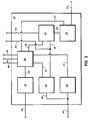
- FIG. 1 is a block diagram of a typical digital computer system with a SCU and associated independent CPU's suitable for incorporating the present invention.
- Figure 2 is a basic flow chart of logic steps for the preferred embodiment of the invention adapted for use with the system shown Figure 1.
- FIG 3 is a typical block diagram of the preferred embodiment of the invention for use with the digital computer system shown in Figure 1.
- Figure 1 shows a typical digital computer system 2 suitable for incorporating the present invention.
- the system 2 includes a system control unit (SCU) 4 with an associated SCU main memory 6 and SCU data storage location directory 8.
- the directory 8 includes a cache consistency unit (CCU) 10 which indicates, for any requested data address from the SCU main memory 6, if the SCU main memory 6 data is superceded by a more current version of the requested data elsewhere in the system 2 with implementation well known in the art.
- CCU cache consistency unit
- the SCU 4 is typically interconnected to a plurality of independent central processing units (CPU's) 12 via individual associated data bus links 14. Each one of the CPU's 12 has a writeback cache 16, a control unit 18 and an input/output (I/O) unit 20.
- CPU's central processing units
- I/O input/output
- the CPU's 12 may individually accept and store data in their associated caches 16. This data may not be in the SCU main memory 6 or may include a refreshed (more current) version of data that is stored in the SCU main memory 6. Also in accordance with the prior art, the addresses of data written into the individual CPU's 12 are transferred to the SCU 4 for storage in the SCU data storage location directory 8, and the CCU 10 indicates which SCU main memory 6 data has been superceded by more current versions in one of the CPU caches 16.
- the above described process of refreshing the SCU main memory 6 with the transferred data generally involves at least the execution of two distinct commands, a "WRITE" command to write the transferred data received by the SCU 4 at a selected address, followed by a "READ” command at the same address.
- the use of two such distinct commands then requires the execution of two complete data transfer timing cycles for the SCU main memory 6, thereby at least doubling memory read latency relative to a single cycle data transfer operation.
- the present invention eliminates memory read latency caused by the need for two distinct commands and two complete data transfer timing cycles for the SCU main memory 6 by using combined operation cycles for the process of transferring the requested data between the CPU's 12 and concurrently storing the transferred data into the SCU main memory 6.
- a "WRITE-PASS" cycle is used. This cycle allows the validated data to be passed through the SCU 4 to the requesting CPU 12 as the validated data is written into the SCU main memory 6.
- a "WRITE-READ" cycle is used.
- This cycle allows only validated portions of the transferred data to be written into the SCU main memory 6, and in the same cycle, for the SCU main memory 6 to be read for transfer of data requested by the requesting one of the CPU's 12.
- the "WRITE-READ" cycle only the validated portion of the data transferred to the SCU 4 in response to the data request from the requesting one of the CPU's 12 is written into the SCU main memory 6, whereas all of the data requested by the requesting one of the CPU's 12 is read from the SCU main memory 6.
- the read data contains the validated portion of the data received by the SCU 4 which was written into the SCU main memory 6.
- the data transferred to the SCU 4 from the located one of the CPU's 12 is transferred into an SCU memory subsystem 22.
- the memory subsystem 22 includes a data write buffer 24, a data bypass multiplexer 26 and a data read buffer 28.
- the memory subsystem 22 serves to sequence and transfer the data transferred to the SCU 4 so that the data flow through the SCU 4 is controlled with the "WRITE-PASS" and "WRITE-READ" operations described above.
- the SCU 8, the SCU main memory 6, the CCU 10, the SCU memory subsystem 22, the write buffer 24, the bypass multiplexer 26 and the read buffer 28 are all components well known in the art. They may be interconnected in a variety of well known configurations, and are shown in block form in Figure 1 for purposes of representation only, since they do not in themselves constitute part of the present invention.
- each CPU 12, the CPU cache 16, the control unit 18 and the I/O unit 20 shown as part of each of the CPU's 12 are well known components which may be interconnected in a variety of well known configurations and are shown in block form for purposes of representation only, since they do not in themselves constitute part of the present invention.
- the methodology of the present invention is shown in the system flow chart of Figure 2.
- the SCU directory 8 determines that the most current version of data requested by a requesting one of the CPU's 12 is not in the SCU main memory 6, but rather in another one of the CPU's 12 located by the SCU directory 8 according to methodology well known in the art.
- the data transferred from the located one of the CPU's 12 with the most current version of the requested data is transferred to the memory subsystem 22 of the SCU 4.
- the SCU 4 command information is processed by the memory subsystem 22 to decode the proper address for selection of the requested data from the SCU main memory 6.
- the selected address is then passed from the memory subsystem 22 to the SCU main memory 6.
- the timing cycle for the SCU main memory 6 is then indicated.
- its validity as the most current version of the requested data is checked in the memory subsystem 22. If the checked data is validated, it is loaded into the write buffer 24 and the write buffer 24 then concurrently transfers the loaded data into both the SCU main memory 6 and the bypass multiplexer 26. If the checked data is not validated by the memory subsystem 22, the data is also loaded into the write buffer 24, but then only the valid portions of the loaded data are written into the SCU main memory 6 at the selected address.
- the memory subsystem 22 indicates a read cycle of the SCU main memory 6 at the selected address.
- the data read from the SCU main memory 6 at the selected address is then a mixture of new validated data transferred from the located one of the CPU's 12 and the old data already stored in the SCU main memory 6.
- the read data is then passed to the bypass multiplexer 26.
- the bypass multiplexer 26 provides a common transfer point for the validated data passed to it directly from the write buffer 24 and the read data at the selected address from the SCU main memory 6.
- the bypass multiplexer 26 transfers either the validated data received from the write buffer 24 or the read data from the selected address of the SCU main memory 6 into the read buffer 28.
- the read buffer 28 then transfers the buffered data to the requesting one of the CPU's 12.
- the requested data is retrieved from the located one of the CPU's 12 and then transferred through the SCU 4 to the requesting one of the CPU's 12 with one of two possible dual operation program cycles which both update the SCU main memory 6 as the requested data is transferred through the SCU 4.
- the data retrieved from the located one of the CPU's 12 is confirmed valid (most current) by the memory subsystem 22, the data is written into the SCU main memory 6 while being transferred through the memory subsystem 22 to the requesting one of the CPU's 12 without any subsequent read cycle of the SCU main memory 6.
- the portions of the retrieved data that can be determined valid are written at the selected address for the requested data in the SCU main memory 6.
- the SCU main memory 6 is then read in its entirety at the same selected address in the same operation, providing read data corresponding to the requested data.
- the read data is a mixture of the valid portions of the data retrieved from the located one of the CPU's 12 along with portions of stored data in the SCU main memory 6 which correspond to the other portions of the requested data.
- the read data forms a complete data transfer of the requested data for the requesting one of the CPU's 12.
- the SCU memory subsystem 22 receives command information from the SCU 4 in an address decoder 30 on a command line 32.
- the address decoder 30 decodes the selected address for storage of the retrieved data in the SCU main memory 6 from the command information.
- the decoded address from the address decoder 30 is fed to a main memory controller 34 via an address line 36.
- the memory controller 34 transmits the selected address into the SCU main memory 6 via a select line 38.
- the memory controller 34 then begins a timing cycle for the SCU main memory 6, with reference clock signals fed to the main memory 6 via a clock line 40 and memory array strobe signals fed to the main memory 6 via a memory array strobe line 42 to lock in the selected address.
- the memory subsystem 22 also includes a validity checker 44 to check the validity of the data retrieved from the located one of the CPU's 12 fed to the validity checker 44 via a validity input line 46.
- the retrieved data is also fed to the write buffer 24 via a write buffer input line 48.
- the write buffer 24 may typically include latching circuitry to latch and store the retrieved data until released by a write data latch signal supplied by the main memory controller 34 and fed to the write buffer 24 via a write buffer latch line 50.
- the validity checker 44 feeds a validity signal to the main memory controller 34 via a validity signal line 52. If the validity signal on the line 52 indicates a valid condition, the main memory controller 34 unlatches the data stored in the write buffer 24 with the write buffer latch signal on the line 50 to feed the unlatched data to the SCU main memory 6 via a write buffer output line 54 at the selected address transmitted to the SCU main memory 6 on the line 38. Concurrently, the main memory controller 34 feeds a multiplexer latch signal to the bypass multiplexer 26 via a multiplexer latch line 56 allowing the data unlatched by the write buffer 24 to pass through the bypass multiplexer 26 via a bypass line 58 into the read buffer 28 via a read buffer input line 60.
- the data fed into the read buffer 28 is latched with a read buffer latch signal on a read buffer latch line 62, and then the latched data is released from the read buffer 28 by the main memory controller 34 at the end of the operation cycle with the read buffer latch signal.
- the data released by the read buffer 28 is then transmitted to the requesting one of the CPU's 12 via a read buffer output line 64.
- the main memory controller 34 If the validity signal on the line 52 does not indicate a valid condition, the main memory controller still unlatches the data stored in the write buffer 24 with the write buffer signal on the line 50, but the main memory controller 34 does not feed the bypass multiplexer 26 with the multiplexer signal on the line 56, so that the released data is only fed to the SCU main memory 6 on the line 54. As is well known, the main memory controller 34 only unlatches those portions of the received data confirmed valid by the validity checker 44.
- the main memory controller 34 commands the SCU main memory 6 to read the data stored at the selected address with a select signal on the line 38.
- the read data from the output of the SCU main memory 6 is fed to the bypass multiplexer 26 via a memory output line 66.
- the bypass multiplexer 26 passes the data read by the SCU main memory 6 to the read buffer 28 via the line 60.
- the data fed into the read buffer 28 is latched with the read buffer latch signal on the line 62, and then the latched data is released from the read buffer 28 by the main memory controller 34 for transmission to the requesting one of the CPU's 12 via the read buffer output line 64.
- the address decoder 30, the memory controller 34 and the validity checker 44 shown in Figure 3 are all well known components which may be interconnected in a variety of well known configurations, and are shown in block form in Figure 3 for purposes of representation only, since they do not in themselves constitute part of the present invention.
- the cycles include one dual operation mode, a "WRITE-BYPASS" cycle, which with transferred data confirmed valid concurrently writes the transferred data into a selected address of the SCU main memory and transfers the data on to the requesting CPU without any intervening read cycle, and another dual operation mode, a "WRITE-READ” cycle, which with transferred data not confirmed valid writes portions of the unconfirmed data which is determined to be valid in the SCU main memory, and then reads the same selected address in the SCU main memory in the same operation, and transmits the read data to the requesting CPU.
Landscapes
- Engineering & Computer Science (AREA)
- Theoretical Computer Science (AREA)
- Physics & Mathematics (AREA)
- General Engineering & Computer Science (AREA)
- General Physics & Mathematics (AREA)
- Memory System Of A Hierarchy Structure (AREA)
- Multi Processors (AREA)
- Static Random-Access Memory (AREA)
Claims (4)
- Système d'ordinateur numérique doté d'une unité de contrôle de système SCU (4) avec une mémoire principale (6) et une pluralité d'unités centrales de traitement (CPU) 12, chacune des CPU ayant sa propre antémémoire à écriture différée (16), un procédé de transfert des données demandées vers celle des CPU qui les a demandées à partir de l'antémémoire d'une desdites autres CPU sélectionnée par le biais de ladite SCU, et de mise à jour de ladite mémoire principale de SCU, comprenant les étapes de :détermination (8) dans ladite SCU que lesdites données demandées sont valides en tant que version la plus récente non en mémoire principale (6), mais dans l'antémémoire de ladite CPU sélectionnée ;transmission desdites données demandées à partir de ladite antémémoire de ladite CPU sélectionnée à ladite SCU ; vérification desdites données transmises pour déterminer que lesdites données transmises sont toutes des données valides ou des données seulement partiellement valides ;si les données transmises sont déterminées comme étant toutes des données valides, alors(a) transmission desdites toutes données valides à ladite CPU qui les a demandées ;
et(b) écriture simultanée desdites toutes données valides dans ladite mémoire principale de SCU à une adresse sélectionnée ; ou,si les données transmises sont déterminées comme étant des données seulement partiellement valides, alors(a) détermination des parties valides desdites données transmises ;(b) écriture seulement des parties valides desdites données dans ladite mémoire principale de SCU à une adresse sélectionnée, tout en lisant, au cours de la même opération, dans ladite mémoire principale de SCU, à ladite adresse sélectionnée, les données étant constituées d'une combinaison de parties valides desdites données transmises avec des parties de données enregistrées dans la mémoire principale correspondant aux autres parties des données demandées ; et(c) transmission desdites données lues à ladite CPU qui les a demandées. - Procédé de transfert selon la revendication 1, comprenant en outre les étapes de :réception (32) des informations de commande de ladite SCU ;décodage (30) d'une adresse mémoire dans ladite mémoire principale pour lesdites données demandées à partir desdites informations de commande ;transmission (36, 34, 40, 42) desdites adresses décodées (38) à ladite mémoire principale ; etmémorisation par déclenchement de ladite adresse décodée dans ladite mémoire principale.
- Système d'ordinateur numérique doté d'une unité de contrôle de système SCU (4) avec une mémoire principale (6) et une pluralité d'unités centrales de traitement (CPU) 12, chacune des CPU ayant sa propre antémémoire à écriture différée (16), un dispositif de transfert des données demandées vers celle des CPU qui les a demandées à partir de l'antémémoire d'une desdites autres CPU sélectionnée par le biais de ladite SCU, et de mise à jour de ladite mémoire principale de SCU, comprenant :un moyen (8) dans ladite SCU pour déterminer que lesdites données demandées sont valides en tant que version la plus récente, non en mémoire principale (6), mais dans l'antémémoire de ladite CPU sélectionnée ;un moyen (16, 18, 48) destiné à transmettre lesdites données demandées à partir de ladite antémémoire de ladite CPU sélectionnée à ladite SCU ;un moyen (44) destiné à vérifier lesdites données transmises pour déterminer que lesdites données transmises sont toutes des données valides ou des données seulement partiellement valides ;un moyen (34, 26, 28) destiné à transmettre lesdites toutes données valides à ladite CPU qui les a demandées ;un moyen (34, 26) destiné à activer l'écriture simultanée desdites toutes données valides dans ladite mémoire principale de SCU à une adresse sélectionnée simultanément à la transmission desdites toutes données valides à ladite CPU qui les a demandées ;un moyen (44) destiné à déterminer les parties valides desdites données partiellement valides ;un moyen (34, 26) destiné à activer l'écriture seulement desdites données partiellement valides dans ladite mémoire principale de SCU à ladite adresse sélectionnée, tout en activant, au cours de la même opération, la lecture dans ladite mémoire principale de SCU, à ladite adresse sélectionnée, des données constituées d'une combinaison de parties valides desdites données transmises avec des parties de données enregistrées dans la mémoire principale correspondant aux autres parties des données demandées ; etun moyen (34, 28) destiné à transmettre lesdites données lues à ladite CPU qui les a demandées.
- Dispositif de transfert selon la revendication 3, comprenant en outre un moyen de réception d'informations de commande depuis ladite SCU ;un moyen (30) destiné à décoder une adresse mémoire dans ladite mémoire principale pour lesdites informations demandées à partir desdites informations de commande ;un moyen (34) destiné à transmettre ladite adresse décodée à ladite mémoire principale ;
etun moyen destiné à mémoriser par déclenchement ladite adresse décodée dans ladite mémoire principale.
Applications Claiming Priority (2)
| Application Number | Priority Date | Filing Date | Title |
|---|---|---|---|
| US07/302,839 US5185875A (en) | 1989-01-27 | 1989-01-27 | Method and apparatus for reducing memory read latency in a shared memory system with multiple processors |
| US302839 | 1989-01-27 |
Publications (3)
| Publication Number | Publication Date |
|---|---|
| EP0379769A2 EP0379769A2 (fr) | 1990-08-01 |
| EP0379769A3 EP0379769A3 (fr) | 1991-06-19 |
| EP0379769B1 true EP0379769B1 (fr) | 1997-09-24 |
Family
ID=23169428
Family Applications (1)
| Application Number | Title | Priority Date | Filing Date |
|---|---|---|---|
| EP89306720A Expired - Lifetime EP0379769B1 (fr) | 1989-01-27 | 1989-07-03 | Cycle de sous-système de mémoire à écriture-lecture/écriture-transmission |
Country Status (6)
| Country | Link |
|---|---|
| US (1) | US5185875A (fr) |
| EP (1) | EP0379769B1 (fr) |
| JP (1) | JPH0642230B2 (fr) |
| AT (1) | ATE158661T1 (fr) |
| CA (1) | CA1323446C (fr) |
| DE (1) | DE68928343T2 (fr) |
Families Citing this family (19)
| Publication number | Priority date | Publication date | Assignee | Title |
|---|---|---|---|---|
| US5371874A (en) * | 1989-01-27 | 1994-12-06 | Digital Equipment Corporation | Write-read/write-pass memory subsystem cycle |
| US5420994A (en) * | 1990-08-06 | 1995-05-30 | Ncr Corp. | Method for reading a multiple byte data element in a memory system with at least one cache and a main memory |
| US5287512A (en) * | 1990-08-06 | 1994-02-15 | Ncr Corporation | Computer memory system and method for cleaning data elements |
| DE69128389T2 (de) * | 1990-09-14 | 1998-06-10 | Digital Equipment Corp | Schreib-Lese/Schreib-Weitergabe-Zyklus für Speicheruntersystem |
| JPH0827755B2 (ja) * | 1991-02-15 | 1996-03-21 | インターナショナル・ビジネス・マシーンズ・コーポレイション | データの単位を高速度でアクセスする方法 |
| US5530835A (en) * | 1991-09-18 | 1996-06-25 | Ncr Corporation | Computer memory data merging technique for computers with write-back caches |
| US5491811A (en) * | 1992-04-20 | 1996-02-13 | International Business Machines Corporation | Cache system using mask bits to recorder the sequences for transfers of data through cache to system memory |
| JP3309425B2 (ja) * | 1992-05-22 | 2002-07-29 | 松下電器産業株式会社 | キャッシュ制御装置 |
| US5862358A (en) * | 1994-12-20 | 1999-01-19 | Digital Equipment Corporation | Method and apparatus for reducing the apparent read latency when connecting busses with fixed read reply timeouts to CPUs with write-back caches |
| US5829052A (en) * | 1994-12-28 | 1998-10-27 | Intel Corporation | Method and apparatus for managing memory accesses in a multiple multiprocessor cluster system |
| JPH08314794A (ja) * | 1995-02-28 | 1996-11-29 | Matsushita Electric Ind Co Ltd | 安定記憶装置へのアクセス待ち時間を短縮するための方法およびシステム |
| US5625778A (en) * | 1995-05-03 | 1997-04-29 | Apple Computer, Inc. | Method and apparatus for presenting an access request from a computer system bus to a system resource with reduced latency |
| US5867642A (en) * | 1995-08-10 | 1999-02-02 | Dell Usa, L.P. | System and method to coherently and dynamically remap an at-risk memory area by simultaneously writing two memory areas |
| JP2814988B2 (ja) * | 1996-04-12 | 1998-10-27 | 日本電気株式会社 | 障害処理方式 |
| US6098115A (en) * | 1998-04-08 | 2000-08-01 | International Business Machines Corporation | System for reducing storage access latency with accessing main storage and data bus simultaneously |
| US6401175B1 (en) * | 1999-10-01 | 2002-06-04 | Sun Microsystems, Inc. | Shared write buffer for use by multiple processor units |
| US7099997B2 (en) * | 2003-02-27 | 2006-08-29 | International Business Machines Corporation | Read-modify-write avoidance using a boundary word storage mechanism |
| US7320063B1 (en) * | 2005-02-04 | 2008-01-15 | Sun Microsystems, Inc. | Synchronization primitives for flexible scheduling of functional unit operations |
| US9037670B2 (en) * | 2012-09-18 | 2015-05-19 | Cisco Technology, Inc. | Ultra low latency network buffer storage |
Family Cites Families (13)
| Publication number | Priority date | Publication date | Assignee | Title |
|---|---|---|---|---|
| US3771137A (en) * | 1971-09-10 | 1973-11-06 | Ibm | Memory control in a multipurpose system utilizing a broadcast |
| FR129151A (fr) * | 1974-02-09 | |||
| US4142234A (en) * | 1977-11-28 | 1979-02-27 | International Business Machines Corporation | Bias filter memory for filtering out unnecessary interrogations of cache directories in a multiprocessor system |
| US4228503A (en) * | 1978-10-02 | 1980-10-14 | Sperry Corporation | Multiplexed directory for dedicated cache memory system |
| JPS55134459A (en) * | 1979-04-06 | 1980-10-20 | Hitachi Ltd | Data processing system |
| US4410944A (en) * | 1981-03-24 | 1983-10-18 | Burroughs Corporation | Apparatus and method for maintaining cache memory integrity in a shared memory environment |
| US4503497A (en) * | 1982-05-27 | 1985-03-05 | International Business Machines Corporation | System for independent cache-to-cache transfer |
| US4695951A (en) * | 1983-07-07 | 1987-09-22 | Honeywell Bull Inc. | Computer hierarchy control |
| US4747043A (en) * | 1984-02-10 | 1988-05-24 | Prime Computer, Inc. | Multiprocessor cache coherence system |
| US4663742A (en) * | 1984-10-30 | 1987-05-05 | International Business Machines Corporation | Directory memory system having simultaneous write, compare and bypass capabilites |
| US4847804A (en) * | 1985-02-05 | 1989-07-11 | Digital Equipment Corporation | Apparatus and method for data copy consistency in a multi-cache data processing unit |
| US4755930A (en) * | 1985-06-27 | 1988-07-05 | Encore Computer Corporation | Hierarchical cache memory system and method |
| US5018063A (en) * | 1988-12-05 | 1991-05-21 | International Business Machines Corporation | Method for reducing cross-interrogate delays in a multiprocessor system |
-
1989
- 1989-01-27 US US07/302,839 patent/US5185875A/en not_active Expired - Lifetime
- 1989-06-12 CA CA000602465A patent/CA1323446C/fr not_active Expired - Fee Related
- 1989-06-28 JP JP1166501A patent/JPH0642230B2/ja not_active Expired - Lifetime
- 1989-07-03 DE DE68928343T patent/DE68928343T2/de not_active Expired - Fee Related
- 1989-07-03 EP EP89306720A patent/EP0379769B1/fr not_active Expired - Lifetime
- 1989-07-03 AT AT89306720T patent/ATE158661T1/de not_active IP Right Cessation
Also Published As
| Publication number | Publication date |
|---|---|
| DE68928343D1 (de) | 1997-10-30 |
| ATE158661T1 (de) | 1997-10-15 |
| EP0379769A3 (fr) | 1991-06-19 |
| US5185875A (en) | 1993-02-09 |
| DE68928343T2 (de) | 1998-05-07 |
| JPH02205964A (ja) | 1990-08-15 |
| JPH0642230B2 (ja) | 1994-06-01 |
| EP0379769A2 (fr) | 1990-08-01 |
| CA1323446C (fr) | 1993-10-19 |
Similar Documents
| Publication | Publication Date | Title |
|---|---|---|
| EP0379769B1 (fr) | Cycle de sous-système de mémoire à écriture-lecture/écriture-transmission | |
| US5659710A (en) | Cache coherency method and system employing serially encoded snoop responses | |
| EP0258559B1 (fr) | Commande de cohérence d'antémémoire avec une mémoire indiquant qu'une lecture est en cours | |
| EP0149355A2 (fr) | Système de traitement de données à cohérence de données | |
| US5623632A (en) | System and method for improving multilevel cache performance in a multiprocessing system | |
| US5696937A (en) | Cache controller utilizing a state machine for controlling invalidations in a network with dual system busses | |
| US7284097B2 (en) | Modified-invalid cache state to reduce cache-to-cache data transfer operations for speculatively-issued full cache line writes | |
| US7971003B2 (en) | Cache coherency in a shared-memory multiprocessor system | |
| EP0526930A1 (fr) | Dispositif à tampon d'interfaçage de processor pour systèmes multiprocesseurs | |
| EP0347040A1 (fr) | Système de mémoire de données | |
| JP2002163148A (ja) | キャッシュメモリー付マルチ処理システム | |
| US6823431B2 (en) | Method for increasing efficiency in a multi-processor system and multi-processor system with increased efficiency | |
| WO1990005953A1 (fr) | Protocole de coherence d'antememoire mis en ×uvre au niveau des equipements avec repertoire distribue et duplique pour multiprocesseurs a hautes performances | |
| US5263144A (en) | Method and apparatus for sharing data between processors in a computer system | |
| JPH04233050A (ja) | キャッシュメモリ交換プロトコル | |
| US5590307A (en) | Dual-port data cache memory | |
| US6516391B1 (en) | Multiprocessor system and methods for transmitting memory access transactions for the same | |
| JPH0532775B2 (fr) | ||
| US5010475A (en) | Consistency ensuring system for the contents of a cache memory | |
| JPH0319976B2 (fr) | ||
| US5371874A (en) | Write-read/write-pass memory subsystem cycle | |
| EP0498520B1 (fr) | Antémémoire de données et procédé de traitement d'erreurs de mémoire pendant réécriture | |
| EP0475730B1 (fr) | Cycle de sous-système de mémoire à écriture-lecture/écriture-transmission | |
| KR100380674B1 (ko) | 멀티프로세서 시스템에서의 기록-통과 기억 동작동안 캐시코히어런스를 유지하는 방법 및 시스템 | |
| JPH0353657B2 (fr) |
Legal Events
| Date | Code | Title | Description |
|---|---|---|---|
| PUAI | Public reference made under article 153(3) epc to a published international application that has entered the european phase |
Free format text: ORIGINAL CODE: 0009012 |
|
| 17P | Request for examination filed |
Effective date: 19890719 |
|
| AK | Designated contracting states |
Kind code of ref document: A2 Designated state(s): AT BE CH DE ES FR GB GR IT LI LU NL SE |
|
| PUAL | Search report despatched |
Free format text: ORIGINAL CODE: 0009013 |
|
| AK | Designated contracting states |
Kind code of ref document: A3 Designated state(s): AT BE CH DE ES FR GB GR IT LI LU NL SE |
|
| 17Q | First examination report despatched |
Effective date: 19941017 |
|
| GRAG | Despatch of communication of intention to grant |
Free format text: ORIGINAL CODE: EPIDOS AGRA |
|
| GRAH | Despatch of communication of intention to grant a patent |
Free format text: ORIGINAL CODE: EPIDOS IGRA |
|
| GRAH | Despatch of communication of intention to grant a patent |
Free format text: ORIGINAL CODE: EPIDOS IGRA |
|
| GRAA | (expected) grant |
Free format text: ORIGINAL CODE: 0009210 |
|
| AK | Designated contracting states |
Kind code of ref document: B1 Designated state(s): AT BE CH DE ES FR GB GR IT LI LU NL SE |
|
| PG25 | Lapsed in a contracting state [announced via postgrant information from national office to epo] |
Ref country code: NL Free format text: LAPSE BECAUSE OF FAILURE TO SUBMIT A TRANSLATION OF THE DESCRIPTION OR TO PAY THE FEE WITHIN THE PRESCRIBED TIME-LIMIT Effective date: 19970924 Ref country code: LI Free format text: LAPSE BECAUSE OF FAILURE TO SUBMIT A TRANSLATION OF THE DESCRIPTION OR TO PAY THE FEE WITHIN THE PRESCRIBED TIME-LIMIT Effective date: 19970924 Ref country code: GR Free format text: LAPSE BECAUSE OF FAILURE TO SUBMIT A TRANSLATION OF THE DESCRIPTION OR TO PAY THE FEE WITHIN THE PRESCRIBED TIME-LIMIT Effective date: 19970924 Ref country code: ES Free format text: THE PATENT HAS BEEN ANNULLED BY A DECISION OF A NATIONAL AUTHORITY Effective date: 19970924 Ref country code: CH Free format text: LAPSE BECAUSE OF FAILURE TO SUBMIT A TRANSLATION OF THE DESCRIPTION OR TO PAY THE FEE WITHIN THE PRESCRIBED TIME-LIMIT Effective date: 19970924 Ref country code: BE Effective date: 19970924 Ref country code: AT Effective date: 19970924 |
|
| REF | Corresponds to: |
Ref document number: 158661 Country of ref document: AT Date of ref document: 19971015 Kind code of ref document: T |
|
| REG | Reference to a national code |
Ref country code: CH Ref legal event code: EP |
|
| REF | Corresponds to: |
Ref document number: 68928343 Country of ref document: DE Date of ref document: 19971030 |
|
| ET | Fr: translation filed | ||
| ITF | It: translation for a ep patent filed | ||
| PG25 | Lapsed in a contracting state [announced via postgrant information from national office to epo] |
Ref country code: SE Effective date: 19971224 |
|
| NLV1 | Nl: lapsed or annulled due to failure to fulfill the requirements of art. 29p and 29m of the patents act | ||
| REG | Reference to a national code |
Ref country code: CH Ref legal event code: PL |
|
| PGFP | Annual fee paid to national office [announced via postgrant information from national office to epo] |
Ref country code: FR Payment date: 19980618 Year of fee payment: 10 |
|
| PGFP | Annual fee paid to national office [announced via postgrant information from national office to epo] |
Ref country code: DE Payment date: 19980625 Year of fee payment: 10 |
|
| PGFP | Annual fee paid to national office [announced via postgrant information from national office to epo] |
Ref country code: GB Payment date: 19980626 Year of fee payment: 10 |
|
| PGFP | Annual fee paid to national office [announced via postgrant information from national office to epo] |
Ref country code: LU Payment date: 19980727 Year of fee payment: 10 |
|
| PLBE | No opposition filed within time limit |
Free format text: ORIGINAL CODE: 0009261 |
|
| STAA | Information on the status of an ep patent application or granted ep patent |
Free format text: STATUS: NO OPPOSITION FILED WITHIN TIME LIMIT |
|
| 26N | No opposition filed | ||
| PG25 | Lapsed in a contracting state [announced via postgrant information from national office to epo] |
Ref country code: LU Free format text: LAPSE BECAUSE OF NON-PAYMENT OF DUE FEES Effective date: 19990703 Ref country code: GB Free format text: LAPSE BECAUSE OF NON-PAYMENT OF DUE FEES Effective date: 19990703 |
|
| PG25 | Lapsed in a contracting state [announced via postgrant information from national office to epo] |
Ref country code: FR Free format text: THE PATENT HAS BEEN ANNULLED BY A DECISION OF A NATIONAL AUTHORITY Effective date: 19990731 |
|
| GBPC | Gb: european patent ceased through non-payment of renewal fee |
Effective date: 19990703 |
|
| PG25 | Lapsed in a contracting state [announced via postgrant information from national office to epo] |
Ref country code: DE Free format text: LAPSE BECAUSE OF NON-PAYMENT OF DUE FEES Effective date: 20000503 |
|
| REG | Reference to a national code |
Ref country code: FR Ref legal event code: ST |
|
| PG25 | Lapsed in a contracting state [announced via postgrant information from national office to epo] |
Ref country code: IT Free format text: LAPSE BECAUSE OF NON-PAYMENT OF DUE FEES;WARNING: LAPSES OF ITALIAN PATENTS WITH EFFECTIVE DATE BEFORE 2007 MAY HAVE OCCURRED AT ANY TIME BEFORE 2007. THE CORRECT EFFECTIVE DATE MAY BE DIFFERENT FROM THE ONE RECORDED. Effective date: 20050703 |