EP0379983A2 - Speicherschnittstellensteuerung - Google Patents
Speicherschnittstellensteuerung Download PDFInfo
- Publication number
- EP0379983A2 EP0379983A2 EP90101055A EP90101055A EP0379983A2 EP 0379983 A2 EP0379983 A2 EP 0379983A2 EP 90101055 A EP90101055 A EP 90101055A EP 90101055 A EP90101055 A EP 90101055A EP 0379983 A2 EP0379983 A2 EP 0379983A2
- Authority
- EP
- European Patent Office
- Prior art keywords
- data
- register
- memory
- mic
- pixel
- Prior art date
- Legal status (The legal status is an assumption and is not a legal conclusion. Google has not performed a legal analysis and makes no representation as to the accuracy of the status listed.)
- Granted
Links
Images


Classifications
-
- G—PHYSICS
- G06—COMPUTING OR CALCULATING; COUNTING
- G06T—IMAGE DATA PROCESSING OR GENERATION, IN GENERAL
- G06T15/00—Three-dimensional [3D] image rendering
- G06T15/10—Geometric effects
- G06T15/30—Clipping
-
- H—ELECTRICITY
- H04—ELECTRIC COMMUNICATION TECHNIQUE
- H04N—PICTORIAL COMMUNICATION, e.g. TELEVISION
- H04N19/00—Methods or arrangements for coding, decoding, compressing or decompressing digital video signals
- H04N19/42—Methods or arrangements for coding, decoding, compressing or decompressing digital video signals characterised by implementation details or hardware specially adapted for video compression or decompression, e.g. dedicated software implementation
- H04N19/423—Methods or arrangements for coding, decoding, compressing or decompressing digital video signals characterised by implementation details or hardware specially adapted for video compression or decompression, e.g. dedicated software implementation characterised by memory arrangements
-
- H—ELECTRICITY
- H04—ELECTRIC COMMUNICATION TECHNIQUE
- H04N—PICTORIAL COMMUNICATION, e.g. TELEVISION
- H04N19/00—Methods or arrangements for coding, decoding, compressing or decompressing digital video signals
- H04N19/60—Methods or arrangements for coding, decoding, compressing or decompressing digital video signals using transform coding
- H04N19/61—Methods or arrangements for coding, decoding, compressing or decompressing digital video signals using transform coding in combination with predictive coding
Definitions
- This invention relates generally to a memory interface controller for use in a digital system and, more particularly, to a VLSI memory interface control apparatus which can operate in synchronous or asynchronous modes and be used in a 3-D color graphics display in real time.
- Three dimensional (3-D) graphics systems are used for providing, for example, video or liquid crystal displays (LCDs) of aeronautical charts and other digitized visual information.
- Performance requirements in such systems demand, among other things, 3-D color graphics in real time, the ability to allow solid objects to remain visible behind transparent objects, high throughput of massive amounts of data and volume clipping of pixels (i.e. the ability to view a scene sliced along the Z axis representative of depth in conventional three-dimensional space).
- Conventional memories do not operate at high enough speeds to meet such requirements.
- no VLSI or other devices are believed to be known in the art which can generate 3-D color graphics in real time for a 20 Hz, 512 x 512 display.
- the invention as characterized in claim 1 overcomes the deficiencies of prior art devices by providing an asynchronous memory interface to maximize system throughput in a 3-D color graphics display system. In addition, all calculations are carried out in a pipeline so that a translucent, Z-buffered pixel can be written every 1 to 2 memory cycles.
- the invention also provides an ability to partition memory which increases effective memory bandwidths while minimizing hardware.
- a memory interface controller (MIC) apparatus for use in a digital system, such as a graphics display system, is disclosed.
- the apparatus comprises means for initializing the system memory, means for receiving incoming pixel data and means for performing hidden surface removal on the incoming pixel data.
- the apparatus further comprises means for construction of images with transparent objects.
- a preferred embodiment of the invention provides a memory interface which writes a translucent, Z-buffered pixel every 1 to 2 memory cycles.
- the invention increases effective memory bandwidths while minimizing memory interface and control hardware.
- the invention provides a means for hidden surface removal on incoming pixel data.
- the invention permits construction of images with transparent objects.
- the invention provides a memory interface control apparatus which can be used in parallel with other similar memory interface controls wherein each control operates independently from the other controls in order to achieve a higher rate of throughput of information.
- the invention provides an apparatus capable of supporting an arbitrary screen size.
- the invention omits writing pixels to memory if they have been volume clipped or Z-clipped to allow for higher throughput.
- FIG. 1 is a block diagram showing schematically the relationship of the memory interface control of the invention to other components in a three dimensional color display graphics system.
- the graphics system includes a microprocessor control (uP) 12, a generic interpolation pipeline processor 14, memory interface control 20, full frame memory (FFM) 22, display electronics 24, and display 26.
- the microprocessor control may be any standard microprocessor suitable for use in high speed graphics applications. In one embodiment of the invention, the microprocessor used was a 68020 as manufactured by Motorola.
- the generic interpolation pipeline processor (GIPP) 14 may be comprised of standard components and is described in more detail hereinbelow.
- the GIPP outputs pixels with a red, green, blue (RGB) value, Z-depth, transparency factor, and priority value rendering an image without respect to where it resides.
- the full frame memory (FFM) 22 may conveniently be a RAM memory suitable for operation with a microprocessor, such as the 68020 model.
- a microprocessor such as the 68020 model.
- each pixel has associated with it X,Y, Z-depth, RGB transparency factor "K" and priority values.
- the X,Y value describes a discrete address where the pixel is to be displayed on the screen.
- the RGB value is then stored at that pixel address.
- the RGB data contains the value which determines, in a color display system, how the red, green and blue color guns are to be driven for the pixel at the location described by X and Y.
- Z-depth, the transparency factor K and the priority value are all useful in determining whether or not the pixel should be written into memory or displayed, for example. Use of these factors by the invention is described in more detail hereinbelow.
- Display 26 in one embodiment of the invention was an LCD display, but may also be a CRT color display, in which case the display electronics would be adapted by well-known means to drive the CRT display.
- the MIC is responsible for building the image. It does this in the following manner:
- the MIC 20 is also capable of:
- the MIC is comprised of the following basic sections: An INPUT INTERFACE, a CLOCK input, a TEST section, CONTROLS, a MICROPROCESSOR INTERFACE (uP INTERFACE), and a MEMORY INTERFACE.
- DATA As is shown in Figure 2, there are 70 bits in the input data bus.
- the data is received in one illustrative application of the invention from the GIPP.
- the data is broken out as shown in Table I herein.
- the DATA inputs are internally pulled down.
- DATA_VALID * This bit is used to indicate that incoming data from the GIPP is valid and is clocked into the MIC during a valid clock enable. A low signal on this line indicates that the data is valid.
- the maximum clock frequency used in one embodiment of the invention is 25 MHz with a 50/50 duty cycle. In this example, all events occur on the rising edge of the clock. The clock speed must not exceed the sum of memory speed plus interface overhead.
- HOLD The HOLD bit stops the MIC pipeline and holds the MIC in its current state. HOLD can be used for system debugging by controlling the MIC to run slower than the clock speed. HOLD is active high. HOLD also stops the preceding stage, i.e. a GIPP in one useful system application. HOLD is asserted synchronously with the clock. This input is internally pulled down.
- the OUTPUT_DIS bit is used to tri-state the output buses. The signal is active high. The outputs shown in Table II herein are tri-stated when this bit is active. This input is internally pulled down.
- the CLEAR* bit commands the MIC to fill the RGB memory, Z-buffer, K-buffer, and Priority buffer with data that has been loaded into the MIC's internal BACKGROUND registers shown in Table III hereinbelow when the memory clear option is enabled.
- These buffers are located in memory devices, such as the full frame memory, which are external to the MIC.
- the Z-buffer may be located in memory 100.
- RG and B may advantageously be double buffered in a "ping-pong" operational scheme.
- CLEAR* has lower priority than commanded Initiated Built-In-Test (IBIT), described below, and scan. If the memory clear option is disabled, the CLEAR* resets the MIC and does not respond with an EMPTY* bit going low. This signal is falling edge sensitive only.
- IBIT Initiated Built-In-Test
- READ/WRITE * The READ/WRITE is asserted by the processor to indicate whether the processor transaction is a read or write. This signal is low for a write and high for a read.
- PADDRESS The address bits from the processor are used to address specific registers within the MIC. The list of registers and associated addresses is given in Table III below. TABLE III PADDRESS Registers ADDRESS REGISTER 0 LOWER_MIC_CONTROLS 1 UPPER_MIC_CONTROLS 2 LOWER_Z_BACKGROUND 3 UPPER_Z_BACKGROUND 4 LOWER_Z_FOREGROUND 5 UPPER_Z_FOREGROUND 6 K AND PRIORITY BACKGROUND 7 RED_BACKGROUND 8 BLUE_BACKGROUND 9 GREEN_BACKGROUND 10 MIC BIST RESULTS 11 RG IBIT RESULTS 12 GB IBIT RESULTS 13 BPL IBIT RESULTS 14 LOWER Z IBIT RESULTS 15 UPPER Z IBIT RESULTS Registers 2, 3, 6, 7, 8 and 9 represent the BACKGROUND registers.
- Registers 10 through 15 are read only.
- the MIC when an image is being built by the MIC, the MIC first initializes the full frame memory by writing the data stored in the background registers at all locations.
- the uP INTERFACE section can control the data content of the background registers. For example, if a blue sky were desired for the display background, the background registers could be set to contain logical "0" values for red and green and a "1" value for blue. Then, when the MIC initializes the system, it will fill the entire image with a blue color. As the image is subsequently built, as in the case, for example, of terrain, the image will always be located in front of the background. Thus, the data comprising the image is written over the background.
- the LOWER_MIC_CONTROL register is formatted in one embodiment of the invention as shown in Figure 4.
- this is a synchronous/asynchronous signal used to configure the MIC so that its inputs can be driven by the preceding stage in a synchronous or asynchronous fashion. If the signal is high, the MIC is driven synchronously, conversely a low signal on this line drives the MIC into asynchronous operation.
- SCREEN_SIZE These bits are used to clip (i.e. crop) the data to the viewable area of the screen.
- the MIC advantageously clips to 512 x 512, 1024 x 1024, 2048 x 2048, or 640 x 512 pixel screens.
- the maximum size of the gaming area described by the input data is 4096 x 4096 pixels. Any pixels outside the viewable area are write inhibited.
- the gaming area size is determined by the GIPP capacity. Those skilled in the art will recognize that many useful combinations of gaming areas and viewable areas are possible employing the teachings of the invention. In one embodiment, it is assumed that (0,0) is in the upper left corner of 4096 x 4096 area.
- Table IV shows the display screen sizes which may be used in combination with the MIC. TABLE IV Screen Sizes DATA DESCRIPTION 00 512 x 512 Display 01 1024 x 1024 Display 10 2048 x 2048 Display 11 640 x 512 Display
- GAM_AREA GAM_AREA . These two bits are used to set the size of the input screen. It is assumed that whatever gaming area size is selected that (0,0) is in the upper left corner. The form is given in Table V. TABLE V Input Screen Size Format BITS INPUT SCREEN SIZE IN NUMBER OF PIXELS 00 512 x 512 01 1024 x 1024 10 2048 x 2048 11 4096 x 4096
- MAX_COUNT These three bits set the maximum amount of memory to be addressed during memory CLEAR and memory IBIT modes of operation. See Table VI.
- the UPPER_MIC_CONTROL register is formatted as shown in Figure 6.
- the BIST bit is used to command the MIC to perform Built-In-Test (BIT) on itself.
- BIT Built-In-Test
- the results are stored in an internal register (Register 10) readable by the processor.
- this signal is asserted high, the EMPTY* bit goes high.
- the EMPTY* signal goes low. This signal takes priority over all other control signals.
- BIST is complete, the BIST bit returns to a low state.
- IBIT_DATA As shown in Figure 5, this bit can command the MIC to test all memory. The MIC loads the background data into all of the memory. Then it reads back and compares this against the background data. All errors are recorded and are readable by the uP. When this bit is asserted high, EMPTY* goes high. It goes low when the test is complete. The BIST bit takes priority over this test. When IBIT_DATA is complete, this bit returns to a low state.
- IBIT_ADDR this bit can command the MIC to perform an address test on all memory. During the address test, the MIC loads an address into each location in memory. It then reads that address and compares the data. To perform this test, the memory must be as wide as the data path, otherwise errors shall result. All errors are recorded and are readable by the uP. When this bit is asserted high, EMPTY* goes low. IBIT_ADDR goes low when the test is complete. BIST and IBIT_DATA take priority over this test.
- MEM_CLR_EN As shown in Figure 5, this bit is used to enable the MIC to clear memory if CLEAR* goes low as indicated by an active high on the MEM_CLR_EN line.
- this bit enables the internal counters independent of any other controls in the MIC. It multiplexes the BIST counter to the lower two bits of green, blue, and Z outputs. It multiplexes the memory clear counter to the X and Y address outputs and the two middle bits of green. This bit is active high.
- BIST_GO/NO_GO * As shown in Figure 5, this bit indicates if any failures were detected during BIST. NO_GO, signifying a test failure, is indicated by a low state. This bit is read only. This bit is valid only if BIST is high.
- CHIP_SEL* Referring again to Figure 2, the CHIP_SEL* is asserted low by the processor when it communicates with the MIC. This signal is internally pulled up.
- this signal resets all registers and internal controls, including the uP status and control registers. This signal is active low. This signal is internally pulled up.
- SCAN_ADDRESS As is understood by those skilled in the art, scan mode is used to test semiconductor chips by driving in a bit pattern and checking for consistent results or “signatures" at the output of the chips. As shown in Figure 2 as part of the TEST section, these two bits are used to select a scan path through the MIC and to enable or disable scan according to the scheme in Table VII below. TABLE VII Scan Address Address Description 00 scan enabled - scan path 0 selected 01 scan enabled - scan path 1 selected 10 scan enabled - scan path 2 selected 11 scan disabled
- this signal is the scan data input. It is internally pulled up.
- PDATA is an 8-bit microprocessor data bus.
- RED is a 6-bit red color memory data bus. This bus is internally pulled down.
- GREEN is a 6-bit green color memory data bus explained in more detail below. This bus is internally pulled down.
- BLUE is a 6-bit blue color memory data bus. This bus is internally pulled down.
- Z is a 16-bit Z-buffer memory data bus which is explained in more detail below. This bus is internally pulled down.
- K is a 3-bit K-buffer memory data bus. This bus is internally pulled down.
- PRIORITY is a 2-bit priority buffer memory data bus. This bus is internally pulled down.
- HALT When HALT is asserted, the stage preceding the MIC must halt until the MIC indicates it is ready for the next pixel. HALT is indicated with a high signal. This signal must go to all GIPPs.
- EMPTY* This bit is used to signify one of the following five modes:
- EMPTY* bit goes low. Once EMPTY* goes low, it shall return high under the following conditions:
- ADDRESS In one embodiment this represents 22 bits which comprise the read and write address for the Z-buffer, RGB memory, K-buffer, and the Priority buffer. There are 11 bits each of X and Y as explained in detail hereinbelow.
- addresses are generated internally. During normal operation, addresses are obtained from register R2, R3, or R7 of the pipeline as shown in Figure 6. Registers R2 and R3 represent read addresses and register R7 represents write addresses.
- WRITE_EN* This is the memory write enable for the RGB memory, Z-buffer, K-buffer, and the Priority buffer. If the signal is low, the data associated with the WRITE* shall be written into memory.
- REG_EN* This signal is used to enable the clock on the register on the output of the memory. This signal and a register with a clock enable must be used in the asynchronous mode. The signal is active low.
- READ* This bit is used to enable a memory output buffer so that memory data is input on the bi-directional memory interface. This signal is active low.
- WRITE* This bit is used to enable a memory input buffer so that data is output to the memory on the clocked interface. Required if the memory is common Input/Output (I/O). The WRITE* signal is active low.
- SCAN_OUT This is the scan output. This signal is tri-stated if scan is not enabled.
- Table VIII shows the pinout totals of one illustrative embodiment of a MIC of the invention. TABLE VIII Pinout INPUTS 85 BI-DIRECTIONAL 47 OUTPUTS 29 POWER 10 GROUND 10 TOTAL 181
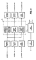
- FIG 11 gives a schematic overview of the MIC Architecture showing the MIC pipeline 70.
- Figure 6 shows in detail a block diagram of the pipeline section 70 of the MIC.
- the first section of the data pipeline is the screen clip portion 30, registers R0 and R1.
- data is latched into register R0. This represents the incoming pixel from the GIPP.
- the X and Y address of the pixel is then used to determine if the pixel is in the viewable area of the screen according to the criteria listed in Table X.
- the maximum size of the gaming area is 4096 x 4096 pixels.
- the maximum screen size is 2048 x 2048 pixels. If the pixel is not in the viewable area, the MIC inhibits the write for that pixel. If the pixel is in the viewable area, the Most Significant Bit (MSB) may require inversion to correctly address the memory. Table X also shows the inversion requirements.
- Table XI hereinbelow demonstrates visually a gaming area size of 4096 x 4096.
- the MIC If the MIC is operating asynchronously, it can read in a pixel on every clock cycle until it gets a pixel in the viewable area. Then, with some exceptions as stated herein, it may only read every other clock cycle. This allows for an increase of system throughput. If the MIC is operating synchronously, it only imports a new pixel to the pipeline every other clock cycle.
- the screen clip section of the MIC rounds the incoming RGB from 8 bits to 6 bits of data for each pixel.
- the next section of the pipeline is the memory read section 32. It is advantageously comprised of registers R2, R3, R4, and R5A and R5B.
- the data is simply being passed along until the corresponding data at the same X and Y address can be fetched from memory.
- data is fetched from memory every second clock cycle and is moved along in the pipeline at the same rate.
- One clock cycle is used to write data out to memory and the other is used to read memory.
- the synchronous mode always works in accordance with the aforedescribed scheme.
- the asynchronous mode may move data along at the clock speed provided that the pixel at the end of the pipeline does not need to be written, or does not need to be read because it is outside the viewable area.
- a write inhibit signal at the output of register R3 is OR'ed with the INHIBIT signal.
- INHIBIT is an internally signal which is set when the state machine detects an address collision.
- the write inhibit bit flows through the pipeline with the rest of the data. At the input to the pipeline, this is called DATA VALID. If the data is valid at the input, this bit is set to a "0" in the example shown. If the pixel is outside of the viewable area, for example, the DATA VALID line will be set high, and the pixel will not be written into memory. This is to prevent the data from register 2 from inadvertently causing an address collision with itself in the pipeline.
- Registers R4 and R5 Connected between Registers R4 and R5 is a 16 word by 10 bit ROM, which is the Look-Up Table (LUT) for K and (1 - K). Because the step size from 7/8 to 1 is not the same as the step size with lower values of K, K should not be interpolated in this range.
- LUT Look-Up Table
- the asynchronous mode requires the use of a register with a clock enable on the output of the memory.
- the last section of the pipeline is the Z-buffering and the alpha channel calculation. It is assumed at this point that the screen clip portion 30 of the pipeline made a decision to write this pixel.
- the Z-buffer 36 checks to see if the pixel Z-depth is less than the Z-depth already in memory. If it is, this pixel is written to the memory. If the screen clip test result is not to write this pixel the Z-buffer test does not change that result. If the two Z-depths are exactly equal, then priority is checked. If the priority of the pixel is less than the priority of the data in memory, the pixel shall be written to the screen. In this way, the Z-depth can be expanded to 18 bits, if required. Also, if the incoming pixel is translucent, K ⁇ 1, and the two Z-depths are equal, the pixel is written. In all other cases, the write is inhibited.
- the alpha channel calculation is performed in two stages 38A and 38B.
- the first stage 38A performs the following two calculations: K*L1, and (1 - K)*L2.
- L1 is the 6 bit value of a specific color of a pixel and L2 is the 8 bit value from memory.
- K is limited to the range of 0 to 1.
- Table XII shows K and its values and (1 - K) and its values.
- the second stage 38B adds the results of the calculations done in the first stage. Upon completion of the alpha calculation, the data is written to memory, provided that the write has not been inhibited at some stage of the pipeline.
- the Address Collision Test 40 compares X and Y addresses at registers R3, R4, R5, and R6 against the address in Register R2. If any one of the addresses matches the address in register R2, the clock enables to registers R1 through R3 and must be halted until the data in the pipeline is flushed out. Also, the GIPP (or GIPPs if more than one is in use) must be halted, otherwise data will be lost at the input to the MIC.
- the MIC If the MIC is in IBIT_DATA mode, it sequentially cycles through all the memory and fill it with the BACKGROUND. Upon completion, it again cycles through all memory reading the data back. If the CLEAR* signal is low, the MIC chip shall cycle through all memory and fill it with the BACKGROUND, provided memory clear is enabled.
- the MIC is in IBIT_ADDR mode, it shall sequentially cycle through all the memory and fill it with addresses. Upon completion, it again cycles through all memory reading the addresses back.
- the uP Control Section comprises two control registers, the background, and status registers.
- the control registers and background registers are described above.
- the status registers contain the results of the various BIT functions.
- IBIT_DATA the MIC shall load background into all of memory and then read the data back in and compare that data against the background. The MIC chip then checks for failed data bits.
- the status registers for IBIT are organized as shown in Figure 7.
- the control registers, the background, and status registers are all reset during a HARD_RESET.
- registers 11 to 15 are reset at the start of IBIT_ADDR and IBIT_DATA.
- the BIST status register (register 10) contains the MIC signature value when BIST is complete. As those skilled in the art will appreciate, this value is dependent upon the specific embodiment of the MIC and the type of built-in self-test used. This is described in more detail below. It is reset at the start of BIST.
- the uP Interface Control shown in Figure 2 generates all control signals to load a register or read a register based on address.
- the Chip Select "CHIP_SEL*
- the read/write signal "READ/WRITE*”
- the uP Input Control Section essentially comprises a 16 byte multiplexer and a 10 byte demultiplexer.
- the PADDRESS lines are used for decoding. If CHIP_SEL* is high, then the demultiplexer outputs must be set in such a state that nothing is selected. If CHIP_SEL* is low, and READ/WRITE* is high, a control or status register on the 16 byte multiplexer 52 is selected (i.e. one of the control/status registers). If READ/WRITE* is low, then a register on the 10 byte demultiplexer is selected (i.e. data is written to one of the control registers). Data is latched when CHIP_SEL goes high.
- Figure 8 schematically shows a block diagram of the MIC Clear Section.
- the logic 60 is designed using well-known logic techniques to carry out the logical relationships between EMPTY* and the other inputs shown in Figure 12 as defined above.
- FIG. 9 schematically shows a block diagram of one embodiment of the IBIT control section of the invention.
- This section contains the Address counter, used to address memory during IBIT modes or CLEAR, and IBIT control.
- This section presents the address counter based on the screen size.
- the counter is preset every time an IBIT mode is commanded or when CLEAR is commanded.
- the address counter is cleared when IBIT is deselected or when clear is complete.
- the other counters are reset when IBIT is deselected.
- the CNT_EN1, RESET1, ADDR_LD, and MIN_ADDR signals are used to control the address generator in the Data Pipeline section. RESET2 resets the status registers.
- IBIT DATA or ADDRESS
- CLEAR When one of the IBIT bits is set high or CLEAR is low, the address counter is preset with an address. This address is a function of MAX_COUNT. It is assumed the minimum memory bank size is 32K. This means the lower 14 bits of the counter shall always be preset to 0. Therefore, only bits 14 - 21 are ever set to a non-zero value.
- Table XIV describes which bits are set to 0 or 1 based on Screen Size and the amount of memory to clear. If TEST is high, all the counters count as four bit counters. This allows the counters to be tested in 16 clock cycles. Scan is also implemented in the counters.
- VLSI logic 62 is designed using well-known logic techniques to implement the above-described logical relationships.
- the counter When IBIT is set high, the counter is preset. When it reaches its maximum counter, it is preset again so the counter runs a second time. The first time is to fill the memory and the second time is to read and compare.
- FIG. 10 is a block diagram of the Clock Control section of the invention.
- the clock circuitry 64 is designed to minimize clock skew. For best results, the clock skew within the MIC must not exceed 2ns.
- the W_INH1 (write inhibit for register R1) signal comes from the Screen Clip section. If the pixel being operated on in that section is not to be written to the screen, this signal is used to indicate that decision to the Clock Control section. This allows the Clock Control section to read another pixel while performing another write to memory (if it is required).
- the W_INH6 (write inhibit for register R6) and W_INH7 (write inhibit for register R7) signals come from the Z and Priority test section. They indicate the pixel in that section is not be written to the screen if it is behind data already in memory. If this occurs, the MIC can then perform back to back reads from memory provided that the incoming pixels are in the viewable area. In the event where the incoming pixel is not in the viewable area and the pixel in the Z and Priority test section are not to be written, a read cycle is performed.
- Using the asynchronous mode allows a higher effective throughput rate. This is due to the fact that as polygons are rendered, surfaces behind surfaces already rendered do not require read-modify-write cycles, but read cycles only. If it is assumed that half the polygons fit into this category then throughput is increased by a factor of 1.5 over the synchronous mode. Maximum throughput in the synchronous case is 12.5 Mpixels/sec. Under the above assumption, throughput could be increased to 18.75 Mpixels/sec., on the average.
- An address collision means that the X,Y address in register R2 of the pipeline is the same as the X,Y address in register R3, R4, R5, or R6 as shown in Figure 6.
- the pipeline must then be cleared out before the pixel in register R2 can be fetched from memory.
- CLK_EN1 must be disabled immediately until the pipeline is emptied. Once an address collision has occurred, the MIC performs write cycles only until the pipeline is empty, then HALT is de-asserted and CLK_EN1 is enabled. Once an address collision has occurred, any subsequent collisions detected are ignored until the pipeline is flushed.
- a signal designated CL1 represents the internal clock used throughout the MIC.
- the routing of this signal must be such that clock skewing is minimized.
- This signal needs strong drive capability because this clock is routed to every stage of the MIC and D Flip Flops (DFFs) are attached to it.
- DFFs D Flip Flops
- the basic philosophy of the clock control state machine design is that all inputs and outputs are registered. All outputs for the next state are determined during the current clock cycle. This means that the effect of any input to the state machine shows up one clock cycle later on the output.
- CLK_EN1 goes high every other clock cycle. A high indicates that the clock is enabled. All of the other clock enables are essentially delayed versions of CLK_EN1.
- CLK_EN2 is one cycle delayed, CLK_EN3 and CLK_EN4 are two cycles delayed and CLK_EN5 is high CUR_R_W is low. This indicates a read cycle.
- HALT is the inverted CLK_EN1 signal. If HOLD is asserted at the state machine inputs (this is one clock cycle after it is asserted external to the part, as this signal must be synchronized) during a write cycle all clock enables are disabled on the next clock cycle, and REG_EN* goes high.
- HOLD On exit from HOLD a read cycle is executed, to pull in the data on the memory output register. The state machine is then back into normal mode. If HOLD is asserted during a read cycle, CLK_EN2 and CLK_EN5 must be asserted during the first cycle of the HOLD so that there is no loss of data. The MIC then switches to a write cycle and REG_EN* is high as in the previous case.
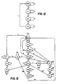
- Figure 12 is a state diagram of the synchronous mode of operation.
- the MIC In the synchronous mode of operation, the MIC has four states, base, H1, H2 and H3. The MIC transitions between these states on paths A through H. Transitions are made according to the synchronous state transition table shown below as Table XV.
- the MIC state diagram is shown in Figure 13.
- the various states are transitioned according asynchronous state transition Table XVI hereinbelow.
- the MIC contains circuitry to perform a deterministic test upon itself and report the results to the host microprocessor. This circuitry utilizes the serial scan paths within the MIC.
- the host microprocessor initiates BIST by setting Bit 0 in the MICs upper control register. Setting this bit enables the BIST Control Logic (BCL).
- BCL BIST Control Logic
- the BCL immediately sets the MIC to a known state by clearing all internal registers and forcing all inputs to a known state.
- An 8-bit linear feedback shift register then generates a pseudo-random serial data stream which is fed into the serial scan paths. When all registers in the serial scan paths have been filled, the registers are taken out of scan mode by de-asserting scan enable.
- the data in the registers is then clocked through the MICs combinatorial logic for one clock cycle.
- the registers are again placed in serial scan mode and the combinatorial results are shifted into a signature analysis register.
- a new pseudo-random pattern is shifted into the registers via the scan path. This process is repeated 16,385 times.
- the result is a pattern in the signature analysis register that is unique to a properly functioning MIC. This pattern is compared to the known MIC signature and the MIC GO/NO_GO in the MIC's test results register is set. Additionally, the MIC signature is available to the host processor via the MIC's BIST results register. The MIC signals that BIST is complete by asserting the EMPTY* output.
- Microprocessor Control section of the MIC sets HARD_RESET low for a short period of time.
- the uP commands Built-in Self-Test (BIST) to be performed on the MIC.
- BIST Built-in Self-Test
- the uP 12 then loads the MIC control and background registers to initialize it. After initialization, the MIC is ready to run.
- the uP then commands the MIC to test memory. These results are stored in the status registers.
- the MIC receives data (address, RGB, K, P, and Z) along with a data valid bit from the MIC. Data valid is active low.
- the MIC controls the rate at which the pipeline in the MIC and GIPP is running. HALT is active high. Whenever this bit is low, the data on the output of the GIPP is loaded into the MIC on the next rising edge of the clock causing the data in the GIPP and MIC to move one register.
- HALT When HALT is high, both the MIC and GIPP shall hold data.
- HALT shall be low every other clock cycle. HALT shall go high for more than one clock whenever the uP control section commands a HOLD or when an address collision occurs in the pipeline. HALT shall go low for more than one clock cycle whenever a screen clip or a Z-clip occurs. This allows for a higher effective throughput.
- the MIC internal design requires that the inputs to and outputs from the memory be registered as shown in Figure 3.
- address and data are driven out of the MIC onto the bus.
- address and data are stored in the register A.
- Register B has its output enabled and is driving data from the previous read cycle into the MIC.
- the data is being written into memory 100 from the previous write cycle (one clock earlier).
- the memory is responsible for generating its own write strobe based on the WRITE_EN* signal. The memory should only write if this signal is low.
Landscapes
- Engineering & Computer Science (AREA)
- Multimedia (AREA)
- Signal Processing (AREA)
- Physics & Mathematics (AREA)
- Geometry (AREA)
- Computer Graphics (AREA)
- General Physics & Mathematics (AREA)
- Theoretical Computer Science (AREA)
- Controls And Circuits For Display Device (AREA)
- Image Generation (AREA)
- Digital Computer Display Output (AREA)
- Image Input (AREA)
Applications Claiming Priority (2)
| Application Number | Priority Date | Filing Date | Title |
|---|---|---|---|
| US07/299,794 US4970636A (en) | 1989-01-23 | 1989-01-23 | Memory interface controller |
| US299794 | 1989-01-23 |
Publications (3)
| Publication Number | Publication Date |
|---|---|
| EP0379983A2 true EP0379983A2 (de) | 1990-08-01 |
| EP0379983A3 EP0379983A3 (de) | 1993-04-07 |
| EP0379983B1 EP0379983B1 (de) | 1997-03-12 |
Family
ID=23156333
Family Applications (1)
| Application Number | Title | Priority Date | Filing Date |
|---|---|---|---|
| EP90101055A Expired - Lifetime EP0379983B1 (de) | 1989-01-23 | 1990-01-19 | Speicherschnittstellensteuerung |
Country Status (4)
| Country | Link |
|---|---|
| US (1) | US4970636A (de) |
| EP (1) | EP0379983B1 (de) |
| JP (1) | JPH02277098A (de) |
| DE (1) | DE69030127T2 (de) |
Cited By (1)
| Publication number | Priority date | Publication date | Assignee | Title |
|---|---|---|---|---|
| EP0731424A1 (de) * | 1995-03-09 | 1996-09-11 | Sharp Kabushiki Kaisha | Gerät zur Wegnahme von verborgenen Flächen mit Z-Puffer |
Families Citing this family (25)
| Publication number | Priority date | Publication date | Assignee | Title |
|---|---|---|---|---|
| JPH0269821A (ja) * | 1988-09-06 | 1990-03-08 | Seiko Epson Corp | 画像表示制御装置 |
| US5222203A (en) * | 1989-01-20 | 1993-06-22 | Daikin Industries, Ltd. | Method and apparatus for displaying translucent surface |
| US5224210A (en) * | 1989-07-28 | 1993-06-29 | Hewlett-Packard Company | Method and apparatus for graphics pipeline context switching in a multi-tasking windows system |
| JPH0371277A (ja) * | 1989-08-10 | 1991-03-27 | Daikin Ind Ltd | サーフェス・モデル描画方法およびその装置 |
| JPH04182696A (ja) * | 1990-11-17 | 1992-06-30 | Nintendo Co Ltd | 画像処理装置 |
| US6034667A (en) * | 1992-01-21 | 2000-03-07 | Radius Inc. | Method and apparatus for displaying YUV color information on a pseudo-color RGB display |
| US5583974A (en) * | 1993-05-10 | 1996-12-10 | Apple Computer, Inc. | Computer graphics system having high performance multiple layer Z-buffer |
| DE4315494C1 (de) * | 1993-05-10 | 1994-09-29 | Daimler Benz Ag | Anordnung und Verfahren zur Programmierung wenigstens eines Kfz-Steuergeräts |
| WO1994027240A1 (en) * | 1993-05-10 | 1994-11-24 | Apple Computer, Inc. | Computer graphics system having high performance multiple layer z-buffer |
| US5519401A (en) * | 1993-11-01 | 1996-05-21 | Loral Corporation | Programmed radar coordinate scan conversion |
| US5742297A (en) * | 1994-11-04 | 1998-04-21 | Lockheed Martin Corporation | Apparatus and method for constructing a mosaic of data |
| US5530450A (en) * | 1995-01-11 | 1996-06-25 | Loral Corporation | Radar scan converter for PPI rectangular and PPI offset rectangular modes |
| JPH0969163A (ja) * | 1995-08-31 | 1997-03-11 | Fujitsu Ltd | コンピュータグラフィックスモデルのポリゴン重なり抽出方法と、ポリゴンのグループ化方法及び装置 |
| US6331856B1 (en) | 1995-11-22 | 2001-12-18 | Nintendo Co., Ltd. | Video game system with coprocessor providing high speed efficient 3D graphics and digital audio signal processing |
| JP3277110B2 (ja) | 1995-12-08 | 2002-04-22 | 株式会社東芝 | 液晶表示装置 |
| US5897666A (en) * | 1996-12-09 | 1999-04-27 | International Business Machines Corporation | Generation of unique address alias for memory disambiguation buffer to avoid false collisions |
| US6577317B1 (en) | 1998-08-20 | 2003-06-10 | Apple Computer, Inc. | Apparatus and method for geometry operations in a 3D-graphics pipeline |
| AU5688199A (en) | 1998-08-20 | 2000-03-14 | Raycer, Inc. | System, apparatus and method for spatially sorting image data in a three-dimensional graphics pipeline |
| US6771264B1 (en) | 1998-08-20 | 2004-08-03 | Apple Computer, Inc. | Method and apparatus for performing tangent space lighting and bump mapping in a deferred shading graphics processor |
| US7599044B2 (en) | 2005-06-23 | 2009-10-06 | Apple Inc. | Method and apparatus for remotely detecting presence |
| US9298311B2 (en) | 2005-06-23 | 2016-03-29 | Apple Inc. | Trackpad sensitivity compensation |
| US7577930B2 (en) | 2005-06-23 | 2009-08-18 | Apple Inc. | Method and apparatus for analyzing integrated circuit operations |
| US7433191B2 (en) | 2005-09-30 | 2008-10-07 | Apple Inc. | Thermal contact arrangement |
| US7598711B2 (en) | 2005-11-23 | 2009-10-06 | Apple Inc. | Power source switchover apparatus and method |
| US9747658B2 (en) * | 2013-09-06 | 2017-08-29 | Apple Inc. | Arbitration method for multi-request display pipeline |
Family Cites Families (3)
| Publication number | Priority date | Publication date | Assignee | Title |
|---|---|---|---|---|
| US4860249A (en) * | 1985-10-04 | 1989-08-22 | Saxpy Computer Corporation | Multizone array processor implementing two sided zone buffers with each side being dynamically configured as a working or I/O side |
| US4821209A (en) * | 1986-01-21 | 1989-04-11 | International Business Machines Corporation | Data transformation and clipping in a graphics display system |
| US4805117A (en) * | 1986-09-26 | 1989-02-14 | International Business Machines Corporation | Method for controlling concatenation of transformation matrices in a graphics display system |
-
1989
- 1989-01-23 US US07/299,794 patent/US4970636A/en not_active Expired - Lifetime
-
1990
- 1990-01-19 DE DE69030127T patent/DE69030127T2/de not_active Expired - Fee Related
- 1990-01-19 EP EP90101055A patent/EP0379983B1/de not_active Expired - Lifetime
- 1990-01-23 JP JP2011961A patent/JPH02277098A/ja active Pending
Non-Patent Citations (1)
| Title |
|---|
| IEEE NAECON (DAYTON) vol. 1, 19 May 1986, NEW-YORK N.Y. US pages 79 - 86 HILL AND KOONCE 'AN EFFICIENT DATA HIERARCHY FOR INTEGRATING BACKGROUD IMAGE INFORMATION IN AN AIRCRAFT MAP SYSTEM' * |
Cited By (2)
| Publication number | Priority date | Publication date | Assignee | Title |
|---|---|---|---|---|
| EP0731424A1 (de) * | 1995-03-09 | 1996-09-11 | Sharp Kabushiki Kaisha | Gerät zur Wegnahme von verborgenen Flächen mit Z-Puffer |
| US5896134A (en) * | 1995-03-09 | 1999-04-20 | Sharp Kabushiki Kaisha | Z buffer hidden surface removal device |
Also Published As
| Publication number | Publication date |
|---|---|
| DE69030127D1 (de) | 1997-04-17 |
| DE69030127T2 (de) | 1997-07-31 |
| JPH02277098A (ja) | 1990-11-13 |
| EP0379983B1 (de) | 1997-03-12 |
| US4970636A (en) | 1990-11-13 |
| EP0379983A3 (de) | 1993-04-07 |
Similar Documents
| Publication | Publication Date | Title |
|---|---|---|
| EP0379983B1 (de) | Speicherschnittstellensteuerung | |
| US6094200A (en) | System and method for accelerated occlusion culling | |
| US6020901A (en) | Fast frame buffer system architecture for video display system | |
| US6999087B2 (en) | Dynamically adjusting sample density in a graphics system | |
| US6975322B2 (en) | Dynamically adjusting a number of rendering passes in a graphics system | |
| US5894572A (en) | Method for process scheduling in a processor based system | |
| JPH0855237A (ja) | フレーム・バッファ・メモリ、グラフィックス・サブシステム、コンピュータ・システム、及び画素のアクセス方法 | |
| JP2908009B2 (ja) | 表示制御方法 | |
| US5444839A (en) | Object based graphics system for rasterizing images in real-time | |
| JP2004280125A (ja) | ビデオ/グラフィックメモリシステム | |
| US7629982B1 (en) | Optimized alpha blend for anti-aliased render | |
| US5880741A (en) | Method and apparatus for transferring video data using mask data | |
| US6760033B2 (en) | Combined floating-point logic core and frame buffer | |
| US5301263A (en) | High memory bandwidth system for updating z-buffer values | |
| JP2952780B2 (ja) | コンピユータ出力システム | |
| JP2004348169A (ja) | グラフィック・システムにおけるサンプル密度および/またはいくつかのレンダリング・パスの動的な調整 | |
| JP3164379B2 (ja) | パレット装置 | |
| EP0148575A2 (de) | Einrichtung und Verfahren zur gleichmässigen horizontalen Verschiebung für einer Videoanzeigegenerator | |
| JP3090714B2 (ja) | 集積回路 | |
| EP0189524B1 (de) | Speichereinheit mit arithmetischen und logischen Funktionen, insbesondere für graphische Datenverarbeitung | |
| JP2883031B2 (ja) | 画面垂直拡大回路及び方法 | |
| US5905821A (en) | Compression/expansion circuit having transfer means and storage means with address management of the storage means | |
| US4703230A (en) | Raster operation circuit | |
| CA1228944A (en) | Video control system | |
| JPS6218595A (ja) | 表示装置 |
Legal Events
| Date | Code | Title | Description |
|---|---|---|---|
| PUAI | Public reference made under article 153(3) epc to a published international application that has entered the european phase |
Free format text: ORIGINAL CODE: 0009012 |
|
| AK | Designated contracting states |
Kind code of ref document: A2 Designated state(s): DE FR GB IT |
|
| PUAL | Search report despatched |
Free format text: ORIGINAL CODE: 0009013 |
|
| AK | Designated contracting states |
Kind code of ref document: A3 Designated state(s): DE FR GB IT |
|
| 17P | Request for examination filed |
Effective date: 19931005 |
|
| GRAG | Despatch of communication of intention to grant |
Free format text: ORIGINAL CODE: EPIDOS AGRA |
|
| 17Q | First examination report despatched |
Effective date: 19960506 |
|
| GRAH | Despatch of communication of intention to grant a patent |
Free format text: ORIGINAL CODE: EPIDOS IGRA |
|
| GRAH | Despatch of communication of intention to grant a patent |
Free format text: ORIGINAL CODE: EPIDOS IGRA |
|
| GRAA | (expected) grant |
Free format text: ORIGINAL CODE: 0009210 |
|
| AK | Designated contracting states |
Kind code of ref document: B1 Designated state(s): DE FR GB IT |
|
| REF | Corresponds to: |
Ref document number: 69030127 Country of ref document: DE Date of ref document: 19970417 |
|
| ET | Fr: translation filed | ||
| ITF | It: translation for a ep patent filed | ||
| PLBE | No opposition filed within time limit |
Free format text: ORIGINAL CODE: 0009261 |
|
| STAA | Information on the status of an ep patent application or granted ep patent |
Free format text: STATUS: NO OPPOSITION FILED WITHIN TIME LIMIT |
|
| 26N | No opposition filed | ||
| REG | Reference to a national code |
Ref country code: GB Ref legal event code: IF02 |
|
| PGFP | Annual fee paid to national office [announced via postgrant information from national office to epo] |
Ref country code: GB Payment date: 20051209 Year of fee payment: 17 |
|
| PGFP | Annual fee paid to national office [announced via postgrant information from national office to epo] |
Ref country code: FR Payment date: 20060104 Year of fee payment: 17 |
|
| PGFP | Annual fee paid to national office [announced via postgrant information from national office to epo] |
Ref country code: IT Payment date: 20060131 Year of fee payment: 17 Ref country code: DE Payment date: 20060131 Year of fee payment: 17 |
|
| PG25 | Lapsed in a contracting state [announced via postgrant information from national office to epo] |
Ref country code: DE Free format text: LAPSE BECAUSE OF NON-PAYMENT OF DUE FEES Effective date: 20070801 |
|
| GBPC | Gb: european patent ceased through non-payment of renewal fee |
Effective date: 20070119 |
|
| REG | Reference to a national code |
Ref country code: FR Ref legal event code: ST Effective date: 20070930 |
|
| PG25 | Lapsed in a contracting state [announced via postgrant information from national office to epo] |
Ref country code: GB Free format text: LAPSE BECAUSE OF NON-PAYMENT OF DUE FEES Effective date: 20070119 |
|
| PG25 | Lapsed in a contracting state [announced via postgrant information from national office to epo] |
Ref country code: FR Free format text: LAPSE BECAUSE OF NON-PAYMENT OF DUE FEES Effective date: 20070131 |
|
| PG25 | Lapsed in a contracting state [announced via postgrant information from national office to epo] |
Ref country code: IT Free format text: LAPSE BECAUSE OF NON-PAYMENT OF DUE FEES Effective date: 20070119 |
|
| P01 | Opt-out of the competence of the unified patent court (upc) registered |
Effective date: 20230525 |