EP0383078B1 - Statischer BICMOS-Speicher mit Funktionsstabilität - Google Patents
Statischer BICMOS-Speicher mit Funktionsstabilität Download PDFInfo
- Publication number
- EP0383078B1 EP0383078B1 EP90101580A EP90101580A EP0383078B1 EP 0383078 B1 EP0383078 B1 EP 0383078B1 EP 90101580 A EP90101580 A EP 90101580A EP 90101580 A EP90101580 A EP 90101580A EP 0383078 B1 EP0383078 B1 EP 0383078B1
- Authority
- EP
- European Patent Office
- Prior art keywords
- bit line
- dummy
- transistors
- dbl
- memory device
- Prior art date
- Legal status (The legal status is an assumption and is not a legal conclusion. Google has not performed a legal analysis and makes no representation as to the accuracy of the status listed.)
- Expired - Lifetime
Links
- 230000015654 memory Effects 0.000 title claims description 81
- 230000003068 static effect Effects 0.000 title description 6
- 238000001514 detection method Methods 0.000 claims description 20
- 230000005669 field effect Effects 0.000 claims description 7
- 238000010586 diagram Methods 0.000 description 9
- 230000000295 complement effect Effects 0.000 description 8
- 239000000872 buffer Substances 0.000 description 5
- 238000007667 floating Methods 0.000 description 5
- 238000004519 manufacturing process Methods 0.000 description 5
- 230000008901 benefit Effects 0.000 description 4
- 239000004020 conductor Substances 0.000 description 4
- 230000001419 dependent effect Effects 0.000 description 4
- 230000000694 effects Effects 0.000 description 4
- 230000009467 reduction Effects 0.000 description 4
- 230000035945 sensitivity Effects 0.000 description 4
- 238000004891 communication Methods 0.000 description 3
- 230000008878 coupling Effects 0.000 description 3
- 238000010168 coupling process Methods 0.000 description 3
- 238000005859 coupling reaction Methods 0.000 description 3
- 230000006872 improvement Effects 0.000 description 3
- 238000000034 method Methods 0.000 description 3
- 230000008520 organization Effects 0.000 description 3
- 230000008859 change Effects 0.000 description 2
- 230000003247 decreasing effect Effects 0.000 description 2
- 239000002184 metal Substances 0.000 description 2
- 230000003071 parasitic effect Effects 0.000 description 2
- 239000007787 solid Substances 0.000 description 2
- 230000003321 amplification Effects 0.000 description 1
- 238000006880 cross-coupling reaction Methods 0.000 description 1
- 238000005516 engineering process Methods 0.000 description 1
- 230000036039 immunity Effects 0.000 description 1
- 238000010348 incorporation Methods 0.000 description 1
- 230000003993 interaction Effects 0.000 description 1
- 238000003199 nucleic acid amplification method Methods 0.000 description 1
- 230000008569 process Effects 0.000 description 1
- 238000011084 recovery Methods 0.000 description 1
- 230000004044 response Effects 0.000 description 1
- 238000012358 sourcing Methods 0.000 description 1
- 230000000087 stabilizing effect Effects 0.000 description 1
Images



Classifications
-
- G—PHYSICS
- G11—INFORMATION STORAGE
- G11C—STATIC STORES
- G11C11/00—Digital stores characterised by the use of particular electric or magnetic storage elements; Storage elements therefor
- G11C11/21—Digital stores characterised by the use of particular electric or magnetic storage elements; Storage elements therefor using electric elements
- G11C11/34—Digital stores characterised by the use of particular electric or magnetic storage elements; Storage elements therefor using electric elements using semiconductor devices
- G11C11/40—Digital stores characterised by the use of particular electric or magnetic storage elements; Storage elements therefor using electric elements using semiconductor devices using transistors
- G11C11/41—Digital stores characterised by the use of particular electric or magnetic storage elements; Storage elements therefor using electric elements using semiconductor devices using transistors forming static cells with positive feedback, i.e. cells not needing refreshing or charge regeneration, e.g. bistable multivibrator or Schmitt trigger
- G11C11/413—Auxiliary circuits, e.g. for addressing, decoding, driving, writing, sensing, timing or power reduction
-
- G—PHYSICS
- G11—INFORMATION STORAGE
- G11C—STATIC STORES
- G11C11/00—Digital stores characterised by the use of particular electric or magnetic storage elements; Storage elements therefor
- G11C11/21—Digital stores characterised by the use of particular electric or magnetic storage elements; Storage elements therefor using electric elements
- G11C11/34—Digital stores characterised by the use of particular electric or magnetic storage elements; Storage elements therefor using electric elements using semiconductor devices
- G11C11/40—Digital stores characterised by the use of particular electric or magnetic storage elements; Storage elements therefor using electric elements using semiconductor devices using transistors
- G11C11/41—Digital stores characterised by the use of particular electric or magnetic storage elements; Storage elements therefor using electric elements using semiconductor devices using transistors forming static cells with positive feedback, i.e. cells not needing refreshing or charge regeneration, e.g. bistable multivibrator or Schmitt trigger
- G11C11/413—Auxiliary circuits, e.g. for addressing, decoding, driving, writing, sensing, timing or power reduction
- G11C11/417—Auxiliary circuits, e.g. for addressing, decoding, driving, writing, sensing, timing or power reduction for memory cells of the field-effect type
- G11C11/419—Read-write [R-W] circuits
Definitions
- This invention is in the field of integrated circuits, and is more specifically directed to a memory device as defined in the precharacterizing part of claim 1.
- a memory device of this type is disclosed in IEEE JOURNAL OF SOLID STATE CIRCUITS, vol 23, no. 5, October 1988, New York, US; HIEP VAN TRAN et al.: "An 8-ns 256K ECL SRAM with CMOS Memory Array and Battery Backup Capability", pages 1041-1047.
- Integrated circuit memory devices are often organized into rows and columns of memory cells, with the rows and columns separately selected based on the value of the portions of the memory address which represent row and column addresses.
- word lines generally refers to a set of conductors of which one, when active, selects the addressed row of memory cells
- bit lines generally refers to a set of conductors which communicate data between memory cells in the addressed row and a sense amplifier.
- the sense amplifier is a circuit which senses the data state of the data on an associated bit line, and which generally amplifies the sensed data state for communication to output stages of the circuit.
- the sense amplifier is formed of a pair of emitter-coupled bipolar transistors, with their bases connected to the complementary bit lines of the column.
- a current source such as an MOS transistor, is connected to the emitters of the pair, so that the differential current received by the bases of the transistors creates a differential collector current through the pair, creating a differential voltage at the collectors which is communicated to a second stage sense amplifier.
- Each of the bit lines in the selected column are actively pulled down; the lower potential bit line is pulled down through the memory cell, and the higher potential bit line is pulled down by the current into the base of the sense amplifier transistor.
- the length and parasitic capacitance of the bit lines also increases. If the capacitance of the bit lines is sufficiently great, the current pulled down into the base of the sense amplifier transistor may not be sufficiently large to fully pull down the bit line at the higher potential, so that the bit line effectively floats. If the bit line which is at the high logic state is effectively floating. power supply noise which couples onto the bit line can raise the potential of the bit line, widening the differential voltage, and slowing the response of the memory if the next cycle reads another memory cell in the same column of the opposite data state.
- Variations in the differential bit line voltage of such a memory are also not desired. Such variations can result from variations in the manufacturing process of the device, resulting in variations in electrical parameters such as the threshold voltage, effective channel length and k′ parameters of the MOS transistors. If the differential bit line voltage is sensitive to these transistor parameters, it is likely that the manufacturing yield of the memory device will be degraded due to performance sensitivity of the device to changes in the manufacturing parameters. Such variations in the differential bit line voltage can also be due to variations in the operating parameters of the device, such as power supply voltage and temperature; if performance is sensitive to variations in these parameters, the specified operating range of the device may be limited.
- the resistance of the bit line between the pull-up resistors and the selected cell can significantly affect the bit line differential voltage. It is preferable to adjust the bit line differential voltage in such a way as to take into consideration the series bit line resistance, as well as to keep the bit line differential voltage constant regardless of the position of the selected cell in the column, so that address-dependent performance variations are not present.
- the memory device having the features of the characterizing part of claim 1 may be incorporated into a BiCMOS SRAM read/write memory having a pair of complementary bit lines associated with each column of memory cells, and a sense amplifier associated with each column.
- the sense amplifiers include emitter-coupled bipolar transistors which have their bases connected to the bit lines of the column, and which have their emitters coupled to a current source.
- Pull-down devices, controlled by the column select signal are connected between the bit lines and the reference supply, so that a pull-down current is maintained, preventing floating of either of the bit lines, maintaining the differential voltage.
- the gates of field-effect transistors that are part of the pull-down devices are controlled simultaneously by the column select signal, so that both devices are operative at the same time.
- a gain control circuit is provided which measures the differential voltage for a dummy column and which adjusts the current flow through the pull-down devices to maintain a relatively constant differential voltage and reduces the sensitivity of the memory device to manufacturing and operating parameters.
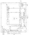
- FIG. 1 is an electrical diagram, in block form, of a static random access memory (SRAM) incorporating the invention.
- SRAM static random access memory
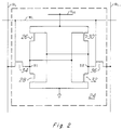
- Figure 2 is an electrical diagram, in schematic form, of a conventional CMOS memory cell as can be used in the SRAM of Figure 1.
- Figure 3 is an electrical diagram, in schematic form, of a bit line pair in conjunction with the bit line pull-up circuitry and first stage sense amplifier.
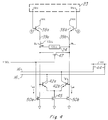
- Figure 4 is an electrical diagram, in schematic form, illustrating the operation of the sense amplifier of the invention during a read cycle.
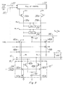
- Figure 5 is an electrical diagram, in schematic form, illustrating a second embodiment of the invention including a gain control circuit for the pull-down current.
- Figure 6 is an electrical diagram, in schematic form, of the gain control circuit of Figure 5.
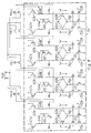
- Figures 7 and 8 are electrical diagrams, in schematic form, of additional embodiments of the bit line differential voltage detection circuit in the gain control circuit of Figure 6.
- Figure 9 is an electrical diagram, in schematic form, of an additional embodiment of the bit line pair of Figure 3.
- SRAM 1 static random access memory
- This embodiment of SRAM 1 is a 1M bit memory, having a single input/output terminal I/O (i.e., SRAM 1 is organized as a 1M by 1 memory).
- the storage elements of SRAM 1 are contained in array 2, which in this embodiment is organized into 512 rows by 2048 columns.
- SRAM 1 receives address information on address inputs A n .
- address inputs A n number nineteen.
- fewer address inputs A n would be required.
- Address inputs A n are received by address buffers 4 which, as is well known in the art, buffer the value of the address externally presented at address inputs A n .
- address buffers 4 which, as is well known in the art, buffer the value of the address externally presented at address inputs A n .
- the remaining ten bits received by address buffers 4, corresponding to a column address are communicated to first stage Y decoder 8, for selection of one of the 2048 columns in array 2 to be sensed by one of the 2048 first stage sense amplifiers 10.
- Each of the 204s columns, and accordingly each of the 2048 first stage sense amplifiers, are associated with a complementary pair of bit lines, as will be described hereinbelow, and the selected one of the 2048 first stage sense amplifiers senses the differential voltage of the complementary bit lines.
- a bank of bit line pull-up transistors 21 are provided in SRAM 1, as will be explained in further detail below.
- Second stage Y decoder 12 Five of the ten column address bits are also communicated to second stage Y decoder 12, for selection of one of the second stage sense amplifiers 14. While Figure 1 illustrates two separate Y decoders 8 and 12, second stage Y decoder 12 may alternatively be inccrporated into first stage Y decoder 8. Such incorporation would use the output of the second stage sense amplifier 14 not only to select the appropriate second stage sense amplifier 14 but also in the decoding of the column address signal to select one of the first stage sense amplifiers 10, if multiple decoding stages are desired within first stage Y decoder 8 and if the break between decode stages therewithin is made at the point necessary to select one of the second stage sense amplifiers 14.
- the 2048 first stage sense amplifiers 10 are grouped into thirty-two groups of thirty-two, with each group having a complementary pair of local data lines 16 as an output.
- One of second stage sense amplifiers 14 is associated with each group of thirty-two first stage sense amplifiers, and receives at its input the associated pair of local data lines 16.
- a complementary pair of data-out lines 18 are driven by second stage sense amplifiers 14.
- the first stage sense amplifier 10 which corresponds to the column address is enabled by a signal from first stage Y decoder 8, while Y decoder 8 disables the others of first stage sense amplifiers 10 from sensing the data state of its associated pair of bit lines from array 2.
- the one of second stage sense amplifiers 14 which corresponds to the group of first stage sense amplifiers 10 having the selected column is also enabled, and the others of second stage sense amplifiers 14 are disabled.
- the selected one of second stage sense amplifiers 14 presents, on data-out lines 18, a differential voltage which is the amplification of the differential voltage on the local data lines 16 at its input, for communication to input/output circuitry 20.
- Input/output circuitry 20 communicates the state of data-out lines 18 to input/output terminal I/O.
- Input/output circuitry 20 of SRAM 1 of Figure 1 also receives input data from input/output terminal I/O; the determination of whether a read or a write cycle is desired depends upon the state of terminal R/W_, connected to input/output circuitry 20.
- input/output circuitry 20 presents the logic state externally presented at input/output terminal I/O onto data-in bus 22, which presents the true and complement states of the input data to first stage sense amplifiers 10 for communication to the selected memory cell in array 2.
- Data-in bus 22 is also connected to pull-up control circuitry 23, to effect the write recovery operation described in further detail hereinbelow.
- SRAM 1 also has reference voltage circuit 24, which receives the power supply voltages V cc and V ee (ground potential). Power supply voltages V cc and V ee are routed to transistors throughout SRAM 1 for biasing purposes, such routing not shown in Figure 1 for purposes of clarity.
- the particular embodiment of SRAM 1 described herein is a BiCMOS SRAM, utilizing both bipolar transistors, as well as p-channel and n-channel MOS transistors. Certain circuits in this emtodiment of SRAM 1 are realized in in emitter-coupled logic. Where emitter-coupled logic is used, reference voltage circuit 24 provides a band-gap reference voltage.
- CMOS static memory cell 24 as incorporated into BiCMOS SRAM 1 is illustrated.
- Memory cell 24 is constructed according to the well-known cross-coupled inverter realization; since both p-channel and n-channel transistors are available, CMOS inverters are used in memory cell 24.
- a first CMOS inverter in memory cell 24 is made up of p-channel transistor 26 and n-channel transistor 28 having their source-to-drain paths connected in series between V cc and ground, and having their gates tied together.
- the second CMOS inverter in memory cell 24 is similarly constructed, with p-channel transistor 30 and n-channel transistor 32 having their source-to-drain paths connected in series between V cc and ground, and their gates also common.
- N-channel pass transistor 34 has its source-to-drain path connected between node S1 and a first bit line BL, and has its gate connected to word line WL.
- N-channel pass transistor 36 similarly has its source-to-drain path connected between node S2 and a second bit line BL_, and has its gate also connected to word line WL.
- node S1 and S2 In operation, the voltages of node S1 and S2 will necessarily be logical complements of one another, due to the cross-coupled nature of the CMOS inverters within memory cell 24.
- the higher of the two nodes S1 and S2 will be pulled high by one of associated p-channel transistors 26 and 30, respectively, and the lower of the two nodes S1 and S2 will be pulled low by one of associated n-channel transistors 28 and 32, respectively.
- the current pulling down the lower of the two nodes S1 and S2 through n-channel transistors 28 and 32, respectively will be referred to as i cell .
- bit lines BL and BL_ When word line WL is energized by X decoder 6 shown in Figure 1, according to the row address received at address inputs A n , pass transistors 34 and 36 will be turned on, coupling nodes S1 and S2 to bit lines BL and BL_, respectively. Accordingly, the state of bit lines BL and BL_ will be logical complements of one another when a memory cell 24 is connected thereto by the energizing of word line WL.
- word lines WL and 2048 pairs of bit lines BL and BL_ there are 512 word lines WL and 2048 pairs of bit lines BL and BL_ in array 2 of Figure 1. For each value of the row address decoded by X decoder 6, one word line WL will be energized, connecting 2048 memory cells 24 to the 2048 pairs of bit lines BL and BL_. Since the other 511 word lines WL will be at a low logic level, only the one memory cell 24 associated with the selected word line WL in each column will be connected to the pair of bit lines BL and BL_ at a time.
- FIG. 3 a column of array 2 is illustrated. Only two memory cells 24 are illustrated, in conjunction with only two word lines WL n and WL n+1 , for purposes of clarity; as described above, each column has 512 memory cells 24 associated with 512 independent word lines WL.
- cells 24 are shown connected to complementary bit lines BL and BL_.
- Bit lines BL and BL_ are connected to first stage sense amplifier 10 and, via n-p-n pull-up transistors 38a and 38b, respectively, to V cc .
- Pull-up transistors 38 correspond to bit line pull-ups 21 shown in Figure 1.
- the bases of pull-up transistors 38a and 38b are driven by pull-up control circuitry 23, which receives clocked input data from input/output circuitry 20 on data-in bus 22.
- the write circuitry for a particular column consists of n-channel transistors 48a and 48b, which have their source-to-drain paths connected in a path between bit lines BL and BL_, respectively, and ground.
- the gates of n-channel transistors 48a and 48b are controlled by data-in lines 22_ and 22, respectively, one of which is taken to a high logic level at the time that a write operation is to occur, with the choice between data-in line 22 and 22_ depending upon the input data received at input/output terminal I/O.
- both data-in lines 22 and 22_ remain at a low logic level.
- N-channel transistors 46a and 46b are connected in series between transistors 48a and 48b, on the one hand, and bit lines BL and BL_, respectively, on the other hand.
- the gates of both of transistors 46a and 46b are controlled by line YSEL, so that the state of data-in lines 22 and 22_ affects only the selected one of the 2048 columns, and is isolated from the other columns.
- First stage sense amplifier 10 consists of two emitter-coupled n-p-n transistors 42a and 42b, which have their bases connected to bit lines BL and BL_, respectively.
- the emitters of transistors 42a and 42b are connected to the drain n-channel transistor 45, which has its source coupled to ground and its gate connected to line YSEL.
- Transistor 45 is turned off when the column is not selected (i.e., line YSEL low), and is turned on to act as a current source when the column is selected (i.e., line YSEL high .
- Line YSEL also is connected to p-channel transistor 47, which serves to equalize bit lines BL and BL_ when transistor 47 is on due to line YSEL low.
- Line YSEL for a particular column, is low during cycles in which the column is not selected, equalizing bit lines BL and BL_.
- the collectors of transistors 42a and 42b are connected to local data lines 16_ and 16, respectively.
- thirty-two first stage sense amplifiers 10 share local data lines 16 and 16_.
- Local data lines 16 and 16a_ are pulled up to V cc by resistors 44, so that the higher of the two bit lines BL and BL_, sourcing the higher base current to its bipolar transistor 42 to cause the higher collector current therethrough, will pull down the local data line 16_ or 16, with the other local data line remaining at a high voltage due to the pull-up resistor 44.
- first stage sense amplifier 10 further has n-channel MOS transistors 50a and 50b.
- Transistors 50a and 50b have their drains connected to the bit lines BL and BL_, respectively, at the bases of transistors 42a and 42b, respectively, and their sources at ground. It should be noted that it is preferred from a layout standpoint that the sources of transistors 50a and 50b be connected to the same reference supply, in this case ground (or V ee ) as transistor 45; of course, the sources of transistors 50a and 50b may be connected to a reference voltage other than that to which the source of transistor 45 is connected, if desired.
- the gates of transistors 50a and 50b are controlled by the state of the column select line YSEL.
- Transistors 50a and 50b are for providing additional pull-down current for the selected column to ensure that the higher potential bit line does not float undesirably high due to power supply or other noise coupling thereto, as will be described hereinbelow.
- line YSEL is in a low logic state, so that transistors 50a and 50b are off and do not draw static current.
- FIG. 4 an equivalent schematic for a selected column in array 2 will be shown, illustrating the benefit of transistors 50a and 50b during a read operation.
- the base of each of pull-up transistors 38a and 38b is biased to V cc for a read operation.
- the voltages at the emitters of pull-up transistors 38a and 38b is thus at V cc -V be .
- the state of cell 24 which is selected is such that a high state will be communicated to bit line BL_ and a low state to bit line BL (i.e., a zero state stored by cell 24).
- the circuit will, of course, operate symmetrically for the opposite data state.
- bit line BL will be pulled low by n-channel transistor 28, with a current to be referred to herein as i cell .
- the higher potential bit line BL_ will be pulled low by the base current into bipolar transistor 42b in sense amplifier 10, with a current to be referred to as i B .
- dV BL (i cell -i B )R39 + V th ln[(i cell +i PD )/(i B +i PD )]
- dV BL is the differential bit line voltage
- R39 is the resistance value of resistors 39a and 39b
- V th is the thermal voltage kT/g (approximately 25 mV at room temperature)
- i PD is the current through each of transistors 50a and 50b.
- the first term of equation (1) is the differential in the voltage drop through resistors 39a and 39b due to the difference in current therethrough; it should of course be noted that i PD also conducts through resistors 39a and 39b, but for purposes of calculating the differential current the voltage drop due to i PD is the same for both resistors 39a and 39b.
- the value of the first term of equation (1) is thus dependent upon the current capability (i.e., the k′ value) of the one of n-channel transistors 28 and 32 which is conducting in the selected memory cell 24.
- the second term of equation (1) is the difference in the base-emitter voltages V be of pull-up transistors 38a and 38b, due to the difference in current sourced thereby.
- i PD is zero, since no pull-down transistors 50a and 50b are present.
- the current capability of the n-channel transistors in the memory cells 24 and also the base current i B thus determine the differential V be .
- This configuration is sufficient insofar as the bipolar transistors 42 can draw sufficient base current to keep the higher potential bit line (bit line BL_ in this example) from floating.
- bit line BL_ bit line
- the parasitic capacitance of the metal or other bit line conductors also increases.
- the increased capacitance presents an increased load to the bipolar transistors 42a and 42b, such an increased load reducing the ability of the transistors 42 to hold down the higher potential bit line, and increasing the likelihood that the bit line can effective float.
- power supply or other noise can couple thereto and increase the bit line differential voltage.
- any differential voltage in the bit lines of the selected column must be discharged prior to the memory cell again establishing the differential current of the correct memory state.
- the time required for the memory cell, and the bipolar transistor 42, to discharge the prior differential voltage thus becomes a factor in the memory access time.
- equalization transistor 47 is provided to equalize bit lines BL and BL_, this transistor 47 only will be turned on when the column is in an unselected state. For high performance SRAMs, if the same column is selected in successive cycles, either transistor 47 will never turn on, or it will only be on for a very short time between cycles which, for a large bit line differential voltage, may be insufficient to discharge the differential from the prior cycle.
- pull-down transistors 50a and 50b are provided in order to provide additional pull-down current to that of the bipolar transistor 42 (in this case 42b which is associated with the higher potential bit line in the selected column. This additional pull-down current will reduce the noise sensitivity of the memory.
- this second term (1) will decrease resulting in a reduction in the value of dV BL .
- sense amplifier 10 senses current rather than differential voltage, so long as a detectable current difference remains, a small bit line differential voltage is not undesirable. Indeed, a small bit line differential voltage is preferred, considering the case of a consecutive read cycles (or a read after a write), where the data state of the selected changes from cycle to cycle. Pull-down transistors 50a and 50b thus provide the benefit of reduction of the bit line differential voltage, allowing fast access time in the subsequent read cycles.
- FIG. 5 a second preferred embodiment of the invention is illustrated which can provide additional stability to the operation of the memory by its control of the current i PD .
- the operating characteristics of the n-channel pull-down transistors 28 and 32 in the memory cell 24 determine the current i cell which pulls down the one of bit lines BL and BL_ having the lower logic level.
- the first term in equation (1) which determines the differential bit line voltage dV BL , and accordingly the value of dV BL itself, is strongly dependent upon the operating characteristics of the n-channel MOS transistors 28 and 32.
- the embodiment of Figure 5 is directed to the adjustment of the current i PD to compensate for variations in the the differential bit line voltage dV BL over a temperature and voltage range, as well as over a range of MOS transistor parameters such as threshold voltage, effective channel length, and k′.
- Sense amplifier 10′ in the embodiment of Figure 5 includes additional n-channel transistors 52a and 52b which are connected in series with transistors 50a and 50b, respectively, between bit lines BL and BL_ and ground.
- the gates of transistors 52a and 52b are controlled by automatic gain control circuit 54.
- the purpose of transistors 52a and 52b is to control the current i PD passing therethrough.
- the differential bit line voltage dV BL can be maintained relatively constant as resistance R BL increases if the second term, which exponentially depends on the current ratio of bit lines BL and BL_, is adjusted accordingly.
- Automatic gain control circuit 54 is intended to accomplish this by reducing the gate voltage of transistors 52 (and thus the source/drain current therethrough) responsive to an increase in R BL , and by increasing the gate voltage of transistors 52 responsive to a decrease in R BL .
- Automatic gain control circuit 54 consists of bit line differential voltage detection circuit 56, having outputs to level shifter 58, which has outputs to an operational amplifier 60.
- the output of op amp 60 is connected to the gates of transistors 52a and 52b, and is also connected in feedback fashion to bit line differential voltage detection circuit 56.
- Bit line differential voltage detection circuit 56 contains, in effect, a dummy column which simulates the operation of a column in array 2, for purposes of determining the proper drive for transistors 52a and 52b.
- This dummy column includes pull-up transistors 62a and 62b, each with their collectors and bases connected to V cc , providing a bias similar to that for pull-up transistors 38a and 38b in array 2.
- Resistors 64a and 64b are connected to the emitters of transistors 62a and 62b, and have a value similar to that of resistors 39a and 39b in array 2.
- N-channel MOS transistors 66 connected in series between bit line DBL and ground, and having their gates tied to V cc , are designed to emulate i cell being drawn by the n-channel MOS transistor in the selected memory cell 24.
- Bit line differential voltage detection circuit 56 further includes a sense amplifier similar sense amplifier 10′, including bipolar transistors 68a and 68b connected in emitter-coupled fashion, having their collectors connected to V cc , their bases connected to dummy bit lines DBL and DBL_, respectively, and their emitters connected in common to the drain of n-channel MOS transistor 70, which has its source connected to ground, to serve as a current source for emitter-coupled transistors 68.
- the gate of transistor 70 is biased to V cc , emulating the selected column in array 2.
- the bases of transistors 68a and 68b, at dummy bit lines DBL and DBL_, are each connected to a cascode pull-down current source, similarly as those in array 2.
- the cascode current sources consist of transistors 74a and 72a connected in series between dummy bit line DBL and ground, and transistors 74b and 72b connected in series between dummy bit line DBL_ and ground.
- the gates of transistors 72 are biased to V cc , to emulate the selected column in array 2.
- the gates of transistors 74 are biased by the output of automatic gain control circuit 54 from op amp 60, which also biases the gates of transistors 52a and 52b in array 2.
- Dummy bit lines DBL and DBL_ are also connected to level shifter circuit 58.
- the purpose of level shifter circuit 58 is to shift the signals on dummy bit lines DBL and DBL_ to the optimum input operating levels of op amp 60, as well as to provide stability in the input to op amp 60 over the operating range of the memory.
- Level shifter 58 includes bipolar transistors 76a and 76b which have their bases connected to bit lines DBL_ and DBL, respectively, and the collectors biased to V cc .
- the emitters of transistors 76a and 76b are connected through resistors 78a and 78b, respectively, to current sources 80a and 80b.
- Resistors 78a and 78b preferably have the same value R78, and are used to define an offset voltage V os , equal to the product of R78 and the difference in the currents provided by current sources 80a and 80b. This offset voltage is selected at the voltage desired for the dummy bit line differential voltage dV DBL .
- Current sources 80a and 80b provide stable reference currents therethrough, and are preferably generated from a band gap reference circuit to obtain temperature and voltage stability for V os .
- An example of a BiCMOS band gap reference circuit is described in my copending patent application US-A- 4 906 863, published 06.03.90, filed February 16, 1988, assigned to Texas Instruments Inccrporated and incorporated herein by this reference.
- Op amp 60 receives the voltage at node N+ between resistor 78b and current source 80b at its non-inverting input, and receives the voltage at node N- between resistor 78a and current source 80a at its inverting input. Due to the constant current sourced by current sources 80a and 80b, the voltage drop across resistors 78a and 78b will remain relatively constant, so long as the base-emitter junctions of transistors 76a and 76b are forward biased so that transistors 76 are on.
- Op amp 60 may be any type of operational amplifier which may be incorporated into the integrated circuit with the memory; since both bipolar and MOS transistors are utilized in the BiCMOS memory described herein, op amp 60 may of course of the BiCMOS type as well, if desired.
- the output of op amp 60 is connected to the gates of transistors 52 in array 2, as well as to the gates of transistors 74 in bit line differential voltage detection circuit 56.
- bit line differential voltage detection circuit 56 In operation, bit line differential voltage detection circuit 56, due to the provision of transistors 66 connected to dummy bit line DBL only, establishes a differential current between dummy bit lines DBL and DBL_, via the operation of emitter-coupled bipolar transistors 68a and 68b and current source 70. As in the case of a selected column in array 2, this will translate into a dummy bit line differential voltage dV DBL (dummy bit line DBL_ being at a high state relative to dummy bit line DBL), according to equation (1) hereinabove. This dummy bit line differential voltage dV DBL is communicated, via level shifter circuit 58, to the inputs of op amp 60.
- the voltage at node N+ will be higher than the voltage at node N-, since node N+ will substantially follow variations in the base voltage of transistor 76b.
- Such a higher dummy bit line differential voltage can be caused by variations in the value of power supply V cc or in the temperature of the memory which cause a variation in the operating characteristics of transistors 66. This situation will cause op amp 60 to increase its output voltage, thereby increasing the voltage at the gates of transistors 52 in array 2, as well as at the gates of transistors 72 in bit line differential voltage detection circuit 56.
- node N+ will be low relative to node N-. This will cause a decrease in the output voltage of op amp 60, in turn resulting in a reduced gate drive to transistors 52 and 74, and thereby a reduction in the currents i PD and i PD ′. The reduction in current i PD will cause an increase in the dummy bit line differential voltage.
- This positive feedback arrangement will eventually result in a dummy bit line differential voltage dV DBL equal to the offset voltage V os of level shifter circuit 58. Since the offset voltage V os is defined by currents from current sources which are relatively stable over a given temperature and voltage range, the offset voltage V os will be similarly stable, and accordingly the differential bit line voltage dV BL will be adjusted to also be relatively stable over the voltage and temperature ranges. In addition, to the extent that the current sources 80a and 80b are stable over a range of MOS transistor threshold voltages, effective channel lengths and k′ values, the offset voltage V os and accordingly the differential bit line voltage dV BL will be held stable by the circuit according to the invention.
- the series resistance of the bit lines BL and BL_ are not considered as a factor in determining the differential bit line voltage dV BL .
- the series resistance of the bit lines BL and BL_ may become significant.
- the bit line resistance in series with the resistors 39a and 39b of Figures 3 and 4 may be especially significant.
- p-channel transistors 26 and 30 in memory cells 24 do not actively pull up the bit line BL or BL_ (depending upon the data state), since the voltage of the high bit line is at V cc -V be due to pull-up transistors 38; accordingly, the source-to-drain voltage of the "on" one of transistors 26 and 30 is not sufficiently greater than the threshold voltage of the transistor to allow the p-channel transistor 26 or 30 to pull up the bit line.
- R BL is limited to the length of the bit line between the selected memory cell 24 and resistor 39, since there is very little current through the portion of the bit line BL or BL_ between the selected memory cell 24 and the base of the associated transistor 42 (thus very little voltage drop thereacross).
- the value of the differential bit line voltage dV BL will also increase.
- FIG. 7 another embodiment of the invention is illustrated which is intended to maintain a relatively constant differential bit line voltage dV BL in the event that the resistance R BL increases due to the selection of a memory cell 24 near sense amplifier 10′ in the selected column.
- the circuit of Figure 7 accomplishes this by adjusting the second term of equation (2) to the extent necessary to compensate for the increase in the first term of equation (2) from the bit line resistance. This is done by adding series resistance into dummy bit lines DBL and DBL_ which corresponds to the series bit line resistance of bit lines BL and BL_ on the high side, and to the portion of the series bit line resistance of bit lines BL and BL_ between the selected memory cell 24 and pull down resistor 39, on the low side.
- the addition of such series resistance into differential bit line voltage detection circuit 56′ of Figure 7 allows compensation of pull-down current i PD according to the series bit line resistance, as well as adjustment of pull-down current i PD according to the address of the selected row.
- FIG. 7 illustrates differential bit line voltage detection circuit 56′ containing multiple dummy memory cells 82.
- cells 82 are for emulating the current i cell drawn by the selected memory cell 24 in array 2.
- Each of dummy memory cells 82 contains a transfer gate 86 connected between dummy bit line DBL and the drain of an n-channel transistor 84 having its gate biased to V cc and its source at ground. Transfer gate 86 connects transistor 84 to dummy bit line DBL responsive to a dummy word line signal DWL received at its gate.
- p-channel transistors 26 and 30 in memory cells 24 do not actively pull up the bit line BL or BL_ (depending upon the data state), since the voltage of the high bit line is at V cc -V be due to pull-up transistors 38; accordingly, the source-to-drain voltage of the "on" one of transistors 26 and 30 is not sufficiently greater than the threshold voltage of the transistor to allow the p-channel transistor 26 or 30 to pull up the bit line. Also as noted above, the portion of dummy bit line DBL between the selected dummy cell 82 and bipolar transistor 68a does not add to the effective series resistance of dummy bit line DBL, since very little current passes therethrough.
- connection dummy bit lines DBL and DBL_ to level shifter circuit 58, near the bases of transistors 68.
- Each of dummy cells 82 thus emulates the characteristics of a selected memory cell 24 in array 2 relative to its connection to bit lines BL and BL_.
- the multiple ones of dummy cells 82 are selected by dummy word lines DWL generated by the row decoder 6 (see Figure 1), according to the row address received on the nine most significant address inputs A n .
- the multiple ones of dummy cells 82 associated with different dummy word lines DWL thus add variable series bit line resistance to dummy bit line DBL in the same fashion that such variable series bit line resistance is added in array 2.
- the remainder of the automatic gain control circuit 54 operates in the same manner as described hereinabove.
- the differential dummy bit line voltage dV DBL will also vary according to equation (2).
- An increase in the series resistance of the dummy bit line DBL would result in a larger differential dummy bit line voltage, which would, via the level shifter circuit 58 described above, present an input to op amp 60 to increase the current i PD through transistors 72 and 52, dropping the differential dummy bit line voltage as well as reducing the differential bit line voltage dV BL in the selected column of array 2.
- the circuit of Figure 7 can thus cause an accurate adjustment in the pull-down current i PD , accordingly stabilizing the differential bit line voltage dV BL over the range of row addresses, and accordingly series bit line resistances, in the memory.
- bit line differential voltage detection circuit 56′ Various techniques for arranging dummy cells 82 can be used, depending upon the space and accuracy constraints of the memory layout. For example, the most accurate emulation of the series bit line resistance in bit line differential voltage detection circuit 56′ would be to have a dummy cell 82 corresponding to each of the rows in array 2; in the 1 Mbit SRAM described hereinabove having 512 rows, 512 dummy cells 82 would be provided within bit line differential voltage detection circuit 56′, with 512 dummy word lines DWL associated in a one-to-one correspondence with the 512 word lines in array 2. A more space efficient technique could alternatively be used, with fewer dummy cells 82.
- bit line differential voltage detection circuit 56′ If, for example, four dummy cells 82 were provided within bit line differential voltage detection circuit 56′, only four dummy word lines DWL would be necessary; row decoder 6 could drive these four dummy word lines DWL in correspondence with the row selected in array 2 by decoding the two most significant row address bits. Such a configuration with fewer dummy cells 82 could provide improved accuracy to a certain degree, with a minimum of necessary circuit area required. Of course, any number of dummy cells 82 ranging from two to the number of actual rows in array 2 may be used; it is of course preferable that the number of dummy cells 82 be a power of 2 so that the decoding of the row address to drive dummy word lines DWL be kept relatively simple.
- Figure 8 illustrates another alternative embodiment of the invention for addressing the effects of increased series bit line resistance due to selection of memory cells 24 near sense amplifier 10′ in array 2.
- differential bit line voltage detection circuit 56 ⁇ has multiple dummy columns, each with transistcrs 66 for emulating the current i cell of the selected memory cell 24.
- the multiple dummy columns each have varying pull-up resistances between the pull-up transistors 62a and the dummy bit line DBL therewithin.
- the varying resistance in series with dummy bit line DBL would be the value of the pull-up resistor 39 plus a resistance value approximately equal to the average series bit line resistance for the memory cells having a row address in the range corresponding to the dummy column.
- the four dummy columns of Figure 8 may correspond to first through fourth quarters of array 2 taken by row address.
- resistors 64a and 64b may have a resistance equal to the sum of resistor 39a in array 2 and one-eighth of the series bit line resistance of one of bit lines BL and BL_
- resistors 64a′ and 64b′ may have a resistance equal to the sum of resistor 39a plus three-eighths of the series bit line resistance of one of bit lines BL and BL_
- resistors 64a ⁇ and 64b ⁇ may have a resistance equal to the sum of resistor 39a plus five-eighths of the series bit line resistance of one of bit lines BL and BL_
- resistors 64a′′′ and 64b′′′ may have a resistance equal to the sum of resistor 39a and seven-eighths of the series bit line resistance of one of bit lines BL and BL_.
- One of the dummy columns is selected according to the decoded row address from row decoder 16, to correspond to the location in the array of the selected memory cell 24 in array 2. This can be done, in the case of four dummy columns, by decoding the two most significant bits of the row address to drive four dummy column select lines DSEL0 through DSEL3. These dummy column select lines can then connect the selected one of the dummy bit line pair DBL and DBL_ to the input of the level shifter circuit 58.
- the unselected ones of the dummy columns may receive the output of op amp 60, but the change in i PD in such columns of course will not be fed back to level shifter circuit 58.
- the dummy column select lines may also be used to control the gates of transistors 74, so that the unselected ones of the dummy columns will not draw DC current when not selected.
- any number of dummy columns may of course be used in the embodiment of Figure 8. It is of course preferable from a decoding standpoint to have a power of 2 as the number of dummy columns.
- FIG. 9 illustrates a column in array 2 which provides n-channel transistors 92a and 92b in series with pull-down transistors 50a and 50b, respectively.
- the gates of transistors 92a and 92b are driven by a digital-to-analog converter 94 which receives the row address from address inputs A n , preferably via an address buffer (not shown), and which presents a voltage at its output corresponding to the received row address value.
- the gates of transistors 92a and 92b can thus be controlled to provide increased i PD in the event that the selected row is near sense amplifier 10 ⁇ (i.e., in the case of an increased series bit line resistance which causes an increased bit line differential voltage dV BL according to equation (2)), and to provide reduced i PD in the event that the selected row is away from sense amplifier 10 ⁇ ( in the case of a decreased series bit line resistance which causes a decreased bit line differential voltage according to equation (2)). Accordingly, the pull-down current can be adjusted directly based on the selected row address.
- Figure 9 illustrates a further improvement to the bit line scheme of the memory.
- the improvement of Figure 9 is especially useful if array 2 is organized into blocks, where a word line is selected only for the block containing the selected (by column address) cell, and where no word line is selected in the other blocks.
- Such block organization is particularly preferable for purposes of reducing power dissipation.
- An example of such block organization for a 1 Mbit SRAM organized as 512 rows by 2048 columns would be the division of the 2048 columns into sixteen blocks of 128 columns each.
- each of the unselected columns in the block having the selected word line will have a memory cell 24 connected to the bit lines BL and BL_, so that one of bit lines BL and BL_ will be pulled down by the corresponding n-channel transistors 28 or 32 in the memory cell 24 in the selected row to a voltage near V cc -V be .
- the equalization provided by transistor 47 between bit lines BL and BL_ in an unselected column will then keep both bit lines BL and BL_ from floating to an undesirably high voltage.
- bit lines BL and BL_ are not pulled down in these columns, noise coupling to bit lines BL and BL_ can raise the potential thereof to an undesirably high level, slowing the performance in a memory cycle selecting a cell in the previously unselected block, as bit lines BL and BL_ must first be discharged before valid data can be sensed.
- the time during which a block of array 2 may remain unselected may be quite large, for example in the case of repeated accesses of data stored in locations having sequential addresses, so that a large number of accesses are performed in one block of array 2.
- the improvement illustrated in Figure 9 provides p-channel transistor 96 connected between bit line BL_ and a reference voltage V cc -V be .
- the voltage of V cc -V be is preferable, as it is the voltage to which the unselected bit lines in the block containing the selected memory cell 24 is biased.
- the gate of transistor 96 is controlled by the columr select line YSEL. In the case of the column not being selected, line YSEL is low, which turns on transistor 47 to equalize the bit lines and, according to this embodiment of the invention, turns on transistor 96 to connect the voltage V cc -V be to the bit lines. Accordingly, transistor 96 provides the additional advantage of keeping the bit lines BL and BL_ from floating during non-selected cycles, thereby reducing time needed in successive cycles for the bit lines BL and BL_ to recover from noise coupled thereto.
- the additional transistor 96 as described above relative to Figure 9, for all columns in array 2, ensures that the potential of the bit lines BL lines are at a desirable potential, regardless of the block organization of array 2.
- the line which provides V cc -V be may come from the bit lines in the selected block, without requiring an external (to array 2) and complicated reference tracking circuit. The resulting bias will be correct across array 2, regardless of operating and process variations. If it is desirable to establish a voltage for unselected bit lines other than V cc -V be , such other voltage may thus be communicated to all bit lines by connection of the bit lines among all blocks as described above.
Landscapes
- Engineering & Computer Science (AREA)
- Microelectronics & Electronic Packaging (AREA)
- Computer Hardware Design (AREA)
- Static Random-Access Memory (AREA)
Claims (18)
- Speichervorrichtung enthaltend:
mehrere Speicherzellen (24), die in Zeilen und Spalten angeordnet sind;
einen Zeilendecodierer (6) zum Auswählen einer Zeile in Abhängigkeit von einem Adressensignal;
mehrere Bitleitungspaare (BL, BL_), wobei jedes der Bitleitungspaare einer Spalte von Speicherzellen zum Übertragen eines Differenzsignals von einer Speicherzelle in der Spalte einer gewählten Zeile zugeordnet ist; und
einen Leseverstärker (10), der mit einem Bitleitungspaar (BL, BL_) verbunden ist, wobei der Leseverstärker enthält:
einen ersten und einen zweiten bipolaren Transistor (42a, 42b), deren Basen mit der ersten und zweiten Bitleitung des Bitleitungspaares (BL, BL_) verbunden sind, und deren Emitter miteinander verbunden sind;
eine Lese-Stromquelle (45), die zwischen den Emittern der bipolaren Transistoren (42a, 42b) und einer ersten Referenzspannung angeschlossen ist; und
eine erste und eine zweite Pull-down-Stromquelle (46a, 46b), die zwischen den Basen des ersten bzw. des zweiten bipolaren Transistors (42a, 42b), und einer zweiten Referenzspannung angeschlossen sind, wobei die erste und die zweite Pull-down-Stromquelle einen ersten bzw. einen zweiten Feldeffekttransistor (46a, 46b) enthalten, und daß
die Gate-Anschlüsse des ersten und des zweiten Feldeffekttransistors (46a, 46b) durch ein Spaltenauswahlsignal (ysel) gesteuert sind, ein erster und ein zweiter Auswahltransistor (48a, 48b) in Reihe mit der ersten bzw. zweiten Pull-down-Stromquelle (46a, 46b) zwischen den Basis-Anschlüssen des ersten und zweiten bipolaren Transistors (42a, 42b) und der zweiten Referenzspannung angeschlossen sind, dadurch gekennzeichnet, daß sie weiterhin eine dritte und eine vierte Pull-down-Stromquelle (50a, 50b) enthält, die einen dritten bzw. einen vierten Feldeffekttransistor (50a, 50b) aufweisen, wobei die dritte und die vierte Stromquelle direkt zwischen den Basis-Anschlüssen des ersten bzw. zweiten bipolaren Transistors und der zweiten Referenzspannung angeschlossen sind, wobei die Gate-Anschlüsse des dritten und vierten Feldeffekttransistors (50a, 50b) durch das Spaltenauswahlsignal (ysel) gesteuert sind. - Speichervorrichtung nach Anspruch 1, dadurch gekennzeichnet, daß die Lese-Stromquelle einen Feldeffekttransistor (45) enthält, dessen Source-Drain-Pfad zwischen den Emittern des ersten und zweiten bipolaren Transistors (42a, 42b) und der ersten Referenzspannung liegt und dessen Gate-Anschluß durch das Spaltenauswahlsignal (ysel) gesteuert ist.
- Speichervorrichtung nach Anspruch 1 oder 2, dadurch gekennzeichnet, daß die ersten und zweiten Referenzspannungen gleich sind.
- Speichervorrichtung nach den Ansprüchen 1, 2 oder 3, dadurch gekennzeichnet, daß sie mehrere Leseverstärker enthält.
- Speichervorrichtung nach Anspruch 4, dadurch gekennzeichnet, daß jeder Leseverstärker einer einzigen Spalte von Speicherzellen zugeordnet ist.
- Speichervorrichtung nach einem der vorigen Ansprüche, dadurch gekennzeichnet, daß sie weiterhin einen Ausgleichstransistor (47) enthält, der jedem Bitleitungspaar zugeordnet ist, wobei der Ausgleichstransistor (47) einen Source-Drain-Pfad aufweist, der mit den Bitleitungen des Bitleitungspaares (BL, BL_) verbunden ist, und dessen Gate-Anschluß durch das Spaltenauswahlsignal (ysel) gesteuert ist, so daß die Bitleitungen des Bitleitungspaares (BL, BL_) in Abhängigkeit von der dazu zugeordneten, nicht ausgewählten Spalte, miteinander verbunden werden.
- Speichervorrichtung nach einem der vorigen Ansprüche, dadurch gekennzeichnet, daß sie weiter einen Vorspannungstransistor (96) enthält, der jedem Bitleitungspaar (BL, BL_) zugeordnet ist, wobei der Source-Drain-Pfad des Vorspannungstransistors (96) zwischen einer Bitleitung seines Bitleitungspaares (BL, BL_) und einer dritten Referenzspannung angeschlossen ist und dessen Gate-Anschluß durch das Spaltenauswahlsignal (ysel) gesteuert ist, so daß das Bitleitungspaar (BL, BL_) in Abhängigkeit von der ihr zugeordneten, die nicht ausgewählten Spalte mit der dritten Referenzspannung verbunden wird.
- Speichervorrichtung nach einem der vorigen Ansprüche, dadurch gekennzeichnet, daß es zusätzlich Mittel (54) zum Steuern des von der ersten und zweiten Pull-down-Stromquelle bereitgestellten Stroms enthält.
- Speichervorrichtung nach Anspruch 8, dadurch gekennzeichnet, daß das Steuermittel Mittel (94) zum Anlegen eines Signals entsprechend der Adresse der gewählten Zeile an die erste und die zweite Pull-down-Stromquelle enthält.
- Speichervorrichtung nach Anspruch 9, dadurch gekennzeichnet, daß das Anlegungsmittel einen Digital-/Analog-Wandler (94) enthält, bei dem ein Ausgang mit den Gate-Anschlüssen des ersten und zweiten Feldeffekttransistors verbunden ist.
- Speichervorrichtung nach Anspruch 8, dadurch gekennzeichnet, daß das Steuermittel enthält:
eine Bitleitungs-Differenzspannungs-Erkennungsschaltung (56), die einen Ausgang aufweist, und
einen Verstärker (60), der ein Ausgangssignal der Bitleitungs-Differenzspannungs-Erkennungsschaltung (56) empfängt und der eine Steuerspannung in Abhängigkeit vom Ausgangssignal der Bitleitungs-Differenzspannungs-Erkennungsschaltung (56) an die erste und zweite Pull-down-Stromquelle anlegt. - Speichervorrichtung nach Anspruch 11, dadurch gekennzeichnet, daß die Bitleitungs-Differenzspannungs-Erkennungsschaltung (56) enthält:
ein Blind-Bitleitungspaar (DBL, DBL_);
Mittel (66) zum Erzeugen eines Differenzsignals auf dem Blind-Bitleitungspaar (DBL, DBL_);
einen Blind-Leseverstärker enthaltend:
einen ersten und zweiten bipolaren Blind-Transistor (68a, 68b), deren Basisanschlüsse mit der ersten und zweiten Blind-Bitleitung des Bitleitungspaares (DBL, DBL_) verbunden sind und deren Emitter miteinander verbunden sind;
eine Blind-Lesestromquelle (70), die zwischen den Emittern der bipolaren Blind-Transistoren (68a, 68b) und der ersten Referenzspannung angeschlossen ist und
eine erste und eine zweite Blind-Pull-down-Stromquelle (74a, 74b), die zwischen der Basis des ersten bzw. zweiten bipolaren Blind-Transistors (68a, 68b) und der zweiten Referenzspannung angeschlossen sind, wobei die erste und die zweite Blind-pull-down-Stromquelle (74a, 74b) durch das Ausgangssignal des Verstärkers gesteuert werden, wobei der Ausgang der Bitleitungs-Differenzspannungs-Erkennungsschaltung (56) das Blind-Bitleitungspaar (DBL, DBL_) enthält. - Speichervorrichtung nach Anspruch 12, dadurch gekennzeichnet, daß sie weiterhin eine Pegelverschiebungsschaltung (58) enthält, die mit dem Blind-Bitleitungspaar (DBL, DBL_) verbunden ist, und mit dem Verstärker zum Bereitstellen eines Signals entsprechend dem Differenzsignal verbunden ist.
- Speichervorrichtung nach Anspruch 13, dadurch gekennzeichnet, daß die Pegelverschiebungsschaltung folgendes enthält:
einen ersten und zweiten Transistor (76a, 76b), die mit der ersten bzw. zweiten Blind-Bitleitung im Blind-Bitleitungspaar (DBL, DBL_) verbunden sind;
einen ersten und zweiten Widerstand (78a, 78b), die mit dem ersten und zweiten Transistor verbunden sind und
eine erste und zweite Pegelverschiebungs-Stromquelle (80a, 80b), die mit dem ersten bzw. zweiten Widerstand (78a, 78b) und einer Referenzspannung verbunden sind. - Speichervorrichtung nach einem der Ansprüche 12 bis 14, dadurch gekennzeichnet, daß das Mittel zum Erzeugen eines Differenzsignals Pull-down-Mittel (66) enthält, die mit einer der Blind-Bitleitungen verbunden sind.
- Speichervorrichtung nach Anspruch 15, dadurch gekennzeichnet, daß das Mittel zum Erzeugen eines Differenzsignals mehrere Pull-down-Mittel enthält, wobei jedes über ein Selektionsgatter mit einer der Blind-Bitleitungen verbunden ist, wobei die Selektionsgatter durch ein Signal gesteuert werden, das der Adresse der ausgewählten Zeile entspricht.
- Speichervorrichtung nach einem der Ansprüche 11 bis 16, dadurch gekennzeichnet, daß die Bitleitungs-Differenzspannungs-Erkennungsschaltung (56) folgendes enthält:
mehrere Blind-Spalten und
eine Auswahlschaltung, die das Blind-Bitleitungspaar (DBL, DBL_) aus einer der Spalten entsprechend der Adresse der ausgewählten Zeile mit dem Verstärker verbindet. - Speichervorrichtung nach einem der vorigen Ansprüche, dadurch gekennzeichnet, daß der erste und der zweite Auswahltransistor (48a, 48b) durch das Spalten-Auswahlsignal (ysel) so gesteuert werden, daß die Basen des ersten und zweiten bipolaren Transistors in Abhängigkeit von der ihnen zugeordneten, nicht ausgewählten Spalte nicht mit der zweiten Referenzspannung verbunden werden.
Applications Claiming Priority (2)
| Application Number | Priority Date | Filing Date | Title |
|---|---|---|---|
| US310796 | 1989-02-14 | ||
| US07/310,796 US4939693A (en) | 1989-02-14 | 1989-02-14 | BiCMOS static memory with improved performance stability |
Publications (2)
| Publication Number | Publication Date |
|---|---|
| EP0383078A1 EP0383078A1 (de) | 1990-08-22 |
| EP0383078B1 true EP0383078B1 (de) | 1995-11-29 |
Family
ID=23204148
Family Applications (1)
| Application Number | Title | Priority Date | Filing Date |
|---|---|---|---|
| EP90101580A Expired - Lifetime EP0383078B1 (de) | 1989-02-14 | 1990-01-26 | Statischer BICMOS-Speicher mit Funktionsstabilität |
Country Status (5)
| Country | Link |
|---|---|
| US (1) | US4939693A (de) |
| EP (1) | EP0383078B1 (de) |
| JP (1) | JP2912659B2 (de) |
| KR (1) | KR900013521A (de) |
| DE (1) | DE69023783T2 (de) |
Families Citing this family (23)
| Publication number | Priority date | Publication date | Assignee | Title |
|---|---|---|---|---|
| JP2583606B2 (ja) * | 1989-05-16 | 1997-02-19 | 富士通株式会社 | センスアンプ回路 |
| JP2646850B2 (ja) * | 1990-11-30 | 1997-08-27 | 日本電気株式会社 | 半導体メモリ回路 |
| US5305268A (en) * | 1990-12-13 | 1994-04-19 | Sgs-Thomson Microelectronics, Inc. | Semiconductor memory with column equilibrate on change of data during a write cycle |
| US5297090A (en) * | 1990-12-13 | 1994-03-22 | Sgs-Thomson Microelectronics, Inc. | Semiconductor memory with column decoded bit line equilibrate |
| US5267197A (en) * | 1990-12-13 | 1993-11-30 | Sgs-Thomson Microelectronics, Inc. | Read/write memory having an improved write driver |
| US5065055A (en) * | 1990-12-20 | 1991-11-12 | Sun Microsystems, Inc. | Method and apparatus for high-speed bi-CMOS differential amplifier with controlled output voltage swing |
| US5325331A (en) * | 1991-04-04 | 1994-06-28 | Micron Technology, Inc. | Improved device for sensing information store in a dynamic memory |
| JP2672721B2 (ja) * | 1991-05-27 | 1997-11-05 | 株式会社東芝 | センスアンプ回路 |
| US5287301A (en) * | 1991-11-25 | 1994-02-15 | Vitesse Semiconductor Corporation | Static RAM cell |
| JP2869260B2 (ja) * | 1992-08-25 | 1999-03-10 | シャープ株式会社 | 半導体記憶装置 |
| US5508964A (en) * | 1993-01-08 | 1996-04-16 | Texas Instruments Incorporated | Write recovery time minimization for Bi-CMOS SRAM |
| US5463580A (en) * | 1993-07-07 | 1995-10-31 | Nec Corproation | Static semiconductor memory device having improved read operation margin and speed |
| JPH0729373A (ja) * | 1993-07-08 | 1995-01-31 | Mitsubishi Electric Corp | 半導体記憶装置 |
| JPH0757475A (ja) * | 1993-08-09 | 1995-03-03 | Nec Corp | 半導体メモリ集積回路装置 |
| JP3068389B2 (ja) * | 1993-09-29 | 2000-07-24 | 日本電気株式会社 | 半導体記憶装置 |
| US5541545A (en) * | 1995-06-07 | 1996-07-30 | International Business Machines Corporation | High speed bipolar D latch circuit with reduced latch clocking output corruption |
| US6141235A (en) * | 1998-07-31 | 2000-10-31 | Texas Instruments Incorporated | Stacked cache memory system and method |
| DE19914489C1 (de) * | 1999-03-30 | 2000-06-08 | Siemens Ag | Vorrichtung zur Bewertung der Zellenwiderstände in einem magnetoresistiven Speicher |
| US6094393A (en) * | 1999-07-29 | 2000-07-25 | Texas Instruments Incorporated | Stacked sense-amp cache memory system and method |
| JP4894095B2 (ja) * | 2001-06-15 | 2012-03-07 | 富士通セミコンダクター株式会社 | 半導体記憶装置 |
| CA2894249C (en) | 2012-12-27 | 2020-03-10 | Keter Plastic Ltd. | Toolbox |
| US11232833B2 (en) * | 2017-08-17 | 2022-01-25 | Arm Limited | Dummy bitline circuitry |
| CN111710355B (zh) * | 2020-05-21 | 2022-05-13 | 中国人民武装警察部队海警学院 | 提升sram芯片写能力的差分电源电路 |
Family Cites Families (16)
| Publication number | Priority date | Publication date | Assignee | Title |
|---|---|---|---|---|
| JPS5847792B2 (ja) * | 1979-07-26 | 1983-10-25 | 富士通株式会社 | ビット線制御回路 |
| JPS593784A (ja) * | 1982-06-30 | 1984-01-10 | Fujitsu Ltd | 半導体記憶装置 |
| JPH0648595B2 (ja) * | 1982-08-20 | 1994-06-22 | 株式会社東芝 | 半導体記憶装置のセンスアンプ |
| JPS5956289A (ja) * | 1982-09-27 | 1984-03-31 | Fujitsu Ltd | 半導体メモリ |
| JPS5968889A (ja) * | 1982-10-08 | 1984-04-18 | Toshiba Corp | 半導体記憶装置 |
| JPS6083291A (ja) * | 1983-10-13 | 1985-05-11 | Nec Corp | 半導体メモリ |
| US4845674A (en) * | 1984-01-11 | 1989-07-04 | Honeywell, Inc. | Semiconductor memory cell including cross-coupled bipolar transistors and Schottky diodes |
| US4607172A (en) * | 1984-02-13 | 1986-08-19 | National Semiconductor Corporation | Bipolar strobed transistor latch for a high gain comparator |
| US4604534A (en) * | 1984-12-03 | 1986-08-05 | International Business Machines Corporation | Highly sensitive high performance sense amplifiers |
| JPS6240689A (ja) * | 1985-08-16 | 1987-02-21 | Fujitsu Ltd | 半導体記憶装置 |
| JP2559028B2 (ja) * | 1986-03-20 | 1996-11-27 | 富士通株式会社 | 半導体記憶装置 |
| US4839862A (en) * | 1986-08-15 | 1989-06-13 | Nec Corporation | Static random access memory having Bi-CMOS construction |
| JPS63146293A (ja) * | 1986-12-09 | 1988-06-18 | Toshiba Corp | 半導体記憶装置 |
| JPS63166090A (ja) * | 1986-12-26 | 1988-07-09 | Toshiba Corp | スタティック型メモリ |
| US4843264A (en) * | 1987-11-25 | 1989-06-27 | Visic, Inc. | Dynamic sense amplifier for CMOS static RAM |
| JPH0817036B2 (ja) * | 1988-10-06 | 1996-02-21 | 日本電気株式会社 | 半導体メモリ回路 |
-
1989
- 1989-02-14 US US07/310,796 patent/US4939693A/en not_active Expired - Lifetime
-
1990
- 1990-01-26 DE DE69023783T patent/DE69023783T2/de not_active Expired - Fee Related
- 1990-01-26 EP EP90101580A patent/EP0383078B1/de not_active Expired - Lifetime
- 1990-02-13 KR KR1019900001766A patent/KR900013521A/ko not_active Abandoned
- 1990-02-14 JP JP2033617A patent/JP2912659B2/ja not_active Expired - Fee Related
Also Published As
| Publication number | Publication date |
|---|---|
| JPH02297797A (ja) | 1990-12-10 |
| KR900013521A (ko) | 1990-09-06 |
| EP0383078A1 (de) | 1990-08-22 |
| DE69023783D1 (de) | 1996-01-11 |
| DE69023783T2 (de) | 1996-04-18 |
| US4939693A (en) | 1990-07-03 |
| JP2912659B2 (ja) | 1999-06-28 |
Similar Documents
| Publication | Publication Date | Title |
|---|---|---|
| US4939693A (en) | BiCMOS static memory with improved performance stability | |
| US5091879A (en) | BiCMOS static memory with improved performance stability | |
| US5093806A (en) | Sensing and decoding scheme for a bicmos read/write memory | |
| US4866674A (en) | Bitline pull-up circuit for a BiCMOS read/write memory | |
| US4862421A (en) | Sensing and decoding scheme for a BiCMOS read/write memory | |
| EP1374248B1 (de) | Cmos speicher mit kleine schwankende spannungen und mit geringer betriebspannung | |
| US4813022A (en) | Static memory with pull-up circuit for pulling-up a potential on a bit line | |
| US5966319A (en) | Static memory device allowing correct data reading | |
| EP0050484B1 (de) | Leseverstärkerschaltung | |
| EP0638903B1 (de) | Lese/Schreibe-Speicher mit negativer rückgekoppelter Blindspeicherschaltung | |
| US5247479A (en) | Current sensing amplifier for SRAM | |
| US5946251A (en) | Bit line equalize circuit of semiconductor memory device | |
| US6424577B2 (en) | Sense amplifier circuit for use in a semiconductor memory device | |
| US7504695B2 (en) | SRAM memory cell and method for compensating a leakage current flowing into the SRAM memory cell | |
| US4899317A (en) | Bit line precharge in a bimos ram | |
| JP3172436B2 (ja) | 半導体メモリ装置の電流センスアンプ回路 | |
| EP0306519B1 (de) | Stromsensitiver differenzverstärker | |
| JPH07147090A (ja) | 半導体メモリ装置 | |
| US5229967A (en) | BICMOS sense circuit for sensing data during a read cycle of a memory | |
| JP2760634B2 (ja) | 集積メモリ | |
| KR950006336B1 (ko) | 반도체 메모리장치의 전류센싱회로 | |
| US5191553A (en) | Semiconductor memory having a plurality of ports | |
| US5168467A (en) | Semiconductor memory device having sense amplifier protection | |
| EP0547892B1 (de) | Integrierte Schaltung mit gegenseitig gesteuerten differenzialen Datenleitungen | |
| US5309400A (en) | Sense circuit for non-volatile memory device |
Legal Events
| Date | Code | Title | Description |
|---|---|---|---|
| PUAI | Public reference made under article 153(3) epc to a published international application that has entered the european phase |
Free format text: ORIGINAL CODE: 0009012 |
|
| AK | Designated contracting states |
Kind code of ref document: A1 Designated state(s): DE FR GB IT NL |
|
| 17P | Request for examination filed |
Effective date: 19901220 |
|
| 17Q | First examination report despatched |
Effective date: 19931115 |
|
| GRAA | (expected) grant |
Free format text: ORIGINAL CODE: 0009210 |
|
| AK | Designated contracting states |
Kind code of ref document: B1 Designated state(s): DE FR GB IT NL |
|
| ITF | It: translation for a ep patent filed | ||
| REF | Corresponds to: |
Ref document number: 69023783 Country of ref document: DE Date of ref document: 19960111 |
|
| ET | Fr: translation filed | ||
| PLBE | No opposition filed within time limit |
Free format text: ORIGINAL CODE: 0009261 |
|
| STAA | Information on the status of an ep patent application or granted ep patent |
Free format text: STATUS: NO OPPOSITION FILED WITHIN TIME LIMIT |
|
| 26N | No opposition filed | ||
| REG | Reference to a national code |
Ref country code: GB Ref legal event code: IF02 |
|
| PGFP | Annual fee paid to national office [announced via postgrant information from national office to epo] |
Ref country code: GB Payment date: 20061213 Year of fee payment: 18 |
|
| PGFP | Annual fee paid to national office [announced via postgrant information from national office to epo] |
Ref country code: DE Payment date: 20070131 Year of fee payment: 18 |
|
| PGFP | Annual fee paid to national office [announced via postgrant information from national office to epo] |
Ref country code: IT Payment date: 20070628 Year of fee payment: 18 |
|
| PGFP | Annual fee paid to national office [announced via postgrant information from national office to epo] |
Ref country code: FR Payment date: 20070103 Year of fee payment: 18 |
|
| PGFP | Annual fee paid to national office [announced via postgrant information from national office to epo] |
Ref country code: NL Payment date: 20071219 Year of fee payment: 19 |
|
| GBPC | Gb: european patent ceased through non-payment of renewal fee |
Effective date: 20080126 |
|
| PG25 | Lapsed in a contracting state [announced via postgrant information from national office to epo] |
Ref country code: DE Free format text: LAPSE BECAUSE OF NON-PAYMENT OF DUE FEES Effective date: 20080801 |
|
| REG | Reference to a national code |
Ref country code: FR Ref legal event code: ST Effective date: 20081029 |
|
| PG25 | Lapsed in a contracting state [announced via postgrant information from national office to epo] |
Ref country code: GB Free format text: LAPSE BECAUSE OF NON-PAYMENT OF DUE FEES Effective date: 20080126 |
|
| PG25 | Lapsed in a contracting state [announced via postgrant information from national office to epo] |
Ref country code: FR Free format text: LAPSE BECAUSE OF NON-PAYMENT OF DUE FEES Effective date: 20080131 |
|
| PG25 | Lapsed in a contracting state [announced via postgrant information from national office to epo] |
Ref country code: IT Free format text: LAPSE BECAUSE OF NON-PAYMENT OF DUE FEES Effective date: 20080126 |
|
| NLV4 | Nl: lapsed or anulled due to non-payment of the annual fee |
Effective date: 20090801 |
|
| PG25 | Lapsed in a contracting state [announced via postgrant information from national office to epo] |
Ref country code: NL Free format text: LAPSE BECAUSE OF NON-PAYMENT OF DUE FEES Effective date: 20090801 |