EP0383210A1 - Dispositif à transfert de charge réalisant une grande efficacité de transfert de charge sans sacrifier la dynamique du signal de sortie - Google Patents
Dispositif à transfert de charge réalisant une grande efficacité de transfert de charge sans sacrifier la dynamique du signal de sortie Download PDFInfo
- Publication number
- EP0383210A1 EP0383210A1 EP90102588A EP90102588A EP0383210A1 EP 0383210 A1 EP0383210 A1 EP 0383210A1 EP 90102588 A EP90102588 A EP 90102588A EP 90102588 A EP90102588 A EP 90102588A EP 0383210 A1 EP0383210 A1 EP 0383210A1
- Authority
- EP
- European Patent Office
- Prior art keywords
- charge transfer
- region
- floating diffusion
- diffusion region
- well
- Prior art date
- Legal status (The legal status is an assumption and is not a legal conclusion. Google has not performed a legal analysis and makes no representation as to the accuracy of the status listed.)
- Granted
Links
Images


Classifications
-
- H—ELECTRICITY
- H10—SEMICONDUCTOR DEVICES; ELECTRIC SOLID-STATE DEVICES NOT OTHERWISE PROVIDED FOR
- H10D—INORGANIC ELECTRIC SEMICONDUCTOR DEVICES
- H10D62/00—Semiconductor bodies, or regions thereof, of devices having potential barriers
- H10D62/10—Shapes, relative sizes or dispositions of the regions of the semiconductor bodies; Shapes of the semiconductor bodies
- H10D62/17—Semiconductor regions connected to electrodes not carrying current to be rectified, amplified or switched, e.g. channel regions
- H10D62/351—Substrate regions of field-effect devices
- H10D62/357—Substrate regions of field-effect devices of FETs
- H10D62/364—Substrate regions of field-effect devices of FETs of IGFETs
- H10D62/378—Contact regions to the substrate regions
-
- H—ELECTRICITY
- H10—SEMICONDUCTOR DEVICES; ELECTRIC SOLID-STATE DEVICES NOT OTHERWISE PROVIDED FOR
- H10D—INORGANIC ELECTRIC SEMICONDUCTOR DEVICES
- H10D62/00—Semiconductor bodies, or regions thereof, of devices having potential barriers
- H10D62/10—Shapes, relative sizes or dispositions of the regions of the semiconductor bodies; Shapes of the semiconductor bodies
- H10D62/17—Semiconductor regions connected to electrodes not carrying current to be rectified, amplified or switched, e.g. channel regions
- H10D62/351—Substrate regions of field-effect devices
- H10D62/357—Substrate regions of field-effect devices of FETs
- H10D62/364—Substrate regions of field-effect devices of FETs of IGFETs
-
- H—ELECTRICITY
- H10—SEMICONDUCTOR DEVICES; ELECTRIC SOLID-STATE DEVICES NOT OTHERWISE PROVIDED FOR
- H10D—INORGANIC ELECTRIC SEMICONDUCTOR DEVICES
- H10D62/00—Semiconductor bodies, or regions thereof, of devices having potential barriers
- H10D62/10—Shapes, relative sizes or dispositions of the regions of the semiconductor bodies; Shapes of the semiconductor bodies
- H10D62/17—Semiconductor regions connected to electrodes not carrying current to be rectified, amplified or switched, e.g. channel regions
- H10D62/351—Substrate regions of field-effect devices
- H10D62/386—Substrate regions of field-effect devices of charge-coupled devices
Definitions
- This invention relates to a charge transfer device and, more particularly, to a configuration of well where a charge transfer line is formed.
- a charge transfer device is operative to transfer data in the form of electric charges from stage to stage and widely used as an image sensor and a delay unit.
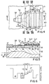
- FIG. 1 A typical example of the charge transfer device is illustrated in Figs. 1 to 3 and fabricated on an n-type semiconductor substrate 1.
- a p-type well 2 In the semiconductor substrate 1 is formed a p-type well 2 where an n-type charge transfer region 3, a floating diffusion region 4 and a drain region 5 are surrounded by a p-type channel stopper region 6.
- a plurality of small p type regions 7 and 8 are formed in the charge transfer region 3 at a predetermined spacing for providing potential barriers between adjacent n-type sub-regions forming parts of a transfer line, and the charge transfer region 3 is covered with an oxide film Ox.
- the n-type charge transfer region 3 extends in the right direction of Figs.
- transfer gate electrodes 9 to 12 and output gate electrodes 13 and 14 which are slightly overlapped with one another, and a reset gate electrode 15 is provided over that area between the floating diffusion region 4 and the drain region 5.
- the transfer gate electrodes 9 and 10 are coupled to a first clock source (not shown) for producing a first phase clock signal CL1, and the transfer gate electrodes 11 and 12 are coupled to a second clock source (not shown) for producing a second phase clock signal CL2.
- the output gate electrodes 13 and 14 are applied with a constant voltage level Vc, and a reset pulse signal CLr is supplied to the reset gate electrode 15.
- the floating diffusion region 4 is balanced in voltage level with the drain region 5 upon application of the reset pulse signal CLr to the reset gate electrode 15.
- the p-type well 2 is grounded, and the semiconductor substrate 1 is positively biased.
- the first and second phase clock signals CL1 and CL2 are alternatively supplied to the transfer gate electrodes 9 to 12, and data signals in the form of electric charges are transferred from the right side to the left side of Fig. 2 in synchronization with the clock signals CL1 and CL2.
- Each data signal finally reaches the sub-region beneath the transfer gate electrode 12, and is further relayed to the floating diffusion region 4 through that area under the output gate electrodes 13 and 14.
- dV SIG Q SIG / C FD
- Q SIG is the amount of electric charges of the data signal
- C FD is the capacitance applied to the floating diffusion region 4.
- the floating diffusion region 4 is smaller in width than the n-type charge transfer region 3, and, for this reason, the ratio of the amount of the electric charges Q SIG to the capacitance C FD is relatively large. This results in the output signal widely swinging its voltage level or a large charge-to-voltage converting gain.
- the present invention proposes to gradually decrease the impurity concentration of a well with channel width.
- a charge transfer device fabricated on a semiconductor substrate of a first conductivity type, comprising: a) a well formed in a surface portion of the semiconductor substrate and having a second conductivity type opposite to the first conductivity type; b) a charge transfer region of the first conductivity type formed in a surface portion of the well; c) a floating diffusion region of the first conductiv ity type formed in the surface portion of the well and contiguous to the charge transfer region; d) an insulating film covering the surface portion of the well; and e) a plurality of gate electrodes provided on the insulating film and applied with driving clocks in such a manner as to produce conductive channels in the charge transfer region for transferring electric charges toward the floating diffusion region, the conductive channels in the vicinity of the floating diffusion region being gradually decreased in width toward the floating diffusion region, in which impurity atoms of the well beneath the charge transfer region in the vicinity of the floating diffusion region are graded toward the floating diffusion region
- a charge coupled device is fabricated on an n-type semiconductor substrate 21, and a p-type well 22 is formed in the semi-conductor substrate 21.
- a p-type well 22 is formed in the p-type well 22 in the p-type well 22 in the p-type well 22 in the p-type well 22 in the p-type well 22 in the p-type well 22 in the p-type well 22 in the p-type well 22 is formed in the p-type well 22 in the p-type well 22 in the p-type well 22 is formed an n-type charge transfer region 23, an n-type floating diffusion region 24 and an n-type drain region 25 which are surrounded by a p-type channel stopper region 26 beneath a thick field oxide film 27. A region between the floating diffusion region 24 and the drain region 25 is of the p-type region.
- the n-type charge transfer region 23 provides a charge transfer line for transferring data signals each in the form of electric charges, and the charge
- a plurality of small p type regions 28 and 29 are formed in the charge transfer region 23 at a predetermined spacing for providing potential barriers between the adjacent charge transfer stages, and the charge transfer region 23 is covered with a thin oxide film 30.
- the n-type charge transfer region 23 extends in the right direction of Figs. 4 and 5 for providing a large number of the charge transfer stages, only two stages located at the terminal end of the transfer line are shown in the figures for the sake of simplicity. In this instance, the charge transfer line terminates at the floating diffusion region 24.
- transfer gate electrodes 31 to 34 and output gate electrodes 35 and 36 two adjacent electrodes of which are slightly overlapped with one another, and a reset gate electrode 37 is provided over that area between the floating diffusion region 24 and the drain region 25.
- the transfer gate electrodes 31 and 32 are coupled to a first clock source (not shown) for producing a first phase clock signal CL11
- the transfer gate electrodes 33 and 34 are coupled to a second clock source (not shown) for producing a second phase clock signal CL12.
- the output gate electrodes 35 and 36 are applied with a constant voltage level Vc, and a reset pulse signal CLr is supplied to the reset gate electrode 37.
- the floating diffusion region 24 is forcibly equalized in voltage level with the drain region 25 upon application of the reset pulse signal CLr to the reset gate electrode 37.
- the p-type well 22 is grounded, and the semiconductor substrate 21 is positively biased by means of a source of positive voltage level 38.
- a source follower amplifier circuit 39 is coupled to the floating diffusion region 24, and the amount of electric charges in the floating diffusion region 24 is proportionally converted into a voltage signal.
- the charge coupled device thus arranged is characterized by the configuration of the p-type well 22, and the p-type well is gradually decreased in depth toward the terminal end of the charge transfer line as will be better seen from Fig. 5.
- the part of the p-type well 22 thus decreased in depth is hereinbelow referred to as "graded region".
- graded region Not only the depth but also p-type impurity concentration are decreased toward the terminal end of the charge transfer line so that the undesirable narrow channel phenomenon is canceled by the graded region even though a channel width W11 of the charge transfer line is reduced toward the terminal end.
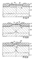
- Such a graded impurity concentration profile is formed as follows. Turning to Figs. 7 to 9 of the drawings, the bottom surface of the p-type well 22 is successively varied. This is because of the fact that the p-type impurity atoms are introduced from both sides of the line V-V through lateral diffusion. If the p-type impurity atoms are laterally diffused from both sides, the impurity concentration is dependent to the distance from the diffusion source. The p-type impurity atoms diffused from the two sources are merged with each other around the center region under the electrodes 33 to 36, however, the p-type well 22 becomes shallow with distance from the sources. This results in that the impurity concentration is decreased with depth of the p-type well toward the terminal end of the charge transfer line.
- FIGs. 12 and 13 of the drawings another charge transfer device according to the present invention is illustrated.
- the charge transfer device shown in Figs. 12 and 13 is similar to that shown in Figs. 4 and 5 with the exception of that p-type region 41 between the n type floating diffusion region 24 and the n-type drain region 25, and, for this reason, other component regions, films and electrodes are labeled with the same reference numerals used in Figs. 4 and 5.
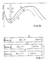
- the p-type region 41 under the resetting gate electrode 37 is graded in the p-type impurity atom concentration, and, for this reason, a declining potential edge takes place in the p-type region 41 as will be seen from Fig. 14.
- the declining potential edge thus produced in the p-type impurity region 41 is advantageous in that electric charges Qr accumulated in the p-type region 41 in the presence of the reset pulse signal CLr are perfectly swept into the drain region 25 when the reset pulse signal CLr disappears. In other words, no electric charge reversely flows into the floating diffusion region 24, and, for this reason, a reset noise is drastically decreased. In this instance, the charge transfer line is prolonged to the p-type region 41.
- the charge transfer device achieves a large charge transfer ratio without any sacrifice of charge-to-voltage converting gain or an output signal range because the declining potential edge cancels the acclivity due to the narrow channel phenomenon.
- the declining potential edge is further operative to produce an electric field along the charge transfer line, so that the electric charges carrying data are accelerated toward the floating diffusion region 24. This results in improvement in operation speed.
- the charge transfer devices described hereinbefore have the respective graded regions at the terminal ends of the charge transfer lines, respectively.
- the declining potential edge may be produced throughout the charge transfer line, and the electric charges are transferred toward the floating diffusion region 24 much faster than the first and second embodiments by the agency of the electric field produced along the charge transfer line.
Landscapes
- Solid State Image Pick-Up Elements (AREA)
Applications Claiming Priority (2)
| Application Number | Priority Date | Filing Date | Title |
|---|---|---|---|
| JP1032430A JPH0728031B2 (ja) | 1989-02-11 | 1989-02-11 | 電荷転送装置 |
| JP32430/89 | 1989-02-11 |
Publications (2)
| Publication Number | Publication Date |
|---|---|
| EP0383210A1 true EP0383210A1 (fr) | 1990-08-22 |
| EP0383210B1 EP0383210B1 (fr) | 1994-04-27 |
Family
ID=12358739
Family Applications (1)
| Application Number | Title | Priority Date | Filing Date |
|---|---|---|---|
| EP90102588A Expired - Lifetime EP0383210B1 (fr) | 1989-02-11 | 1990-02-09 | Dispositif à transfert de charge réalisant une grande efficacité de transfert de charge sans sacrifier la dynamique du signal de sortie |
Country Status (4)
| Country | Link |
|---|---|
| US (1) | US5103278A (fr) |
| EP (1) | EP0383210B1 (fr) |
| JP (1) | JPH0728031B2 (fr) |
| DE (1) | DE69008378T2 (fr) |
Cited By (1)
| Publication number | Priority date | Publication date | Assignee | Title |
|---|---|---|---|---|
| WO2002059975A1 (fr) * | 2001-01-23 | 2002-08-01 | Koninklijke Philips Electronics N.V. | Dispositif a couplage de charge |
Families Citing this family (9)
| Publication number | Priority date | Publication date | Assignee | Title |
|---|---|---|---|---|
| JPH04247629A (ja) * | 1991-02-01 | 1992-09-03 | Fujitsu Ltd | 電荷結合デバイス及びその製造方法 |
| JP3070146B2 (ja) * | 1991-06-19 | 2000-07-24 | ソニー株式会社 | 固体撮像装置 |
| JPH05243281A (ja) * | 1992-03-02 | 1993-09-21 | Nec Corp | 半導体装置及びその製造方法 |
| JP2500436B2 (ja) * | 1993-05-10 | 1996-05-29 | 日本電気株式会社 | 信号処理装置 |
| JP2768311B2 (ja) * | 1995-05-31 | 1998-06-25 | 日本電気株式会社 | 電荷転送装置 |
| US6417531B1 (en) * | 1998-11-24 | 2002-07-09 | Nec Corporation | Charge transfer device with final potential well close to floating diffusion region |
| JP2001044416A (ja) * | 1999-07-28 | 2001-02-16 | Sony Corp | 電荷転送装置及び固体撮像装置 |
| JP5243983B2 (ja) * | 2009-01-30 | 2013-07-24 | 浜松ホトニクス株式会社 | 電子増倍機能内蔵型の固体撮像素子 |
| KR101508283B1 (ko) * | 2010-06-01 | 2015-04-07 | 볼리 미디어 커뮤니케이션스 (센젠) 캄파니 리미티드 | 감광소자 및 그 리딩 방법, 리딩 회로 |
Citations (1)
| Publication number | Priority date | Publication date | Assignee | Title |
|---|---|---|---|---|
| US4698656A (en) * | 1985-02-27 | 1987-10-06 | Nec Corporation | Output detector of a charge coupled device |
Family Cites Families (8)
| Publication number | Priority date | Publication date | Assignee | Title |
|---|---|---|---|---|
| US3796932A (en) * | 1971-06-28 | 1974-03-12 | Bell Telephone Labor Inc | Charge coupled devices employing nonuniform concentrations of immobile charge along the information channel |
| FR2259437A1 (en) * | 1974-01-24 | 1975-08-22 | Commissariat Energie Atomique | Composite conducting layer charge coupled device - provides asymmetric potential well using alternate oppositely doped regions |
| US4499590A (en) * | 1981-12-03 | 1985-02-12 | Westinghouse Electric Corp. | Semiconductor circuit for compressing the dynamic range of a signal |
| JPS5965470A (ja) * | 1982-10-05 | 1984-04-13 | Nec Corp | 電荷結合素子の出力構造 |
| FR2597647B1 (fr) * | 1986-04-18 | 1992-06-12 | Thomson Csf | Registre a decalage a transfert de charge muni d'un dispositif de lecture en tension sur diode flottante |
| US4862235A (en) * | 1988-06-30 | 1989-08-29 | Tektronix, Inc. | Electrode structure for a corner turn in a series-parallel-series charge coupled device |
| US4992842A (en) * | 1988-07-07 | 1991-02-12 | Tektronix, Inc. | Charge-coupled device channel with countinously graded built-in potential |
| US4910569A (en) * | 1988-08-29 | 1990-03-20 | Eastman Kodak Company | Charge-coupled device having improved transfer efficiency |
-
1989
- 1989-02-11 JP JP1032430A patent/JPH0728031B2/ja not_active Expired - Lifetime
-
1990
- 1990-02-09 EP EP90102588A patent/EP0383210B1/fr not_active Expired - Lifetime
- 1990-02-09 DE DE69008378T patent/DE69008378T2/de not_active Expired - Fee Related
-
1991
- 1991-04-29 US US07/693,164 patent/US5103278A/en not_active Expired - Lifetime
Patent Citations (1)
| Publication number | Priority date | Publication date | Assignee | Title |
|---|---|---|---|---|
| US4698656A (en) * | 1985-02-27 | 1987-10-06 | Nec Corporation | Output detector of a charge coupled device |
Non-Patent Citations (1)
| Title |
|---|
| PATENT ABSTRACTS OF JAPAN * |
Cited By (2)
| Publication number | Priority date | Publication date | Assignee | Title |
|---|---|---|---|---|
| WO2002059975A1 (fr) * | 2001-01-23 | 2002-08-01 | Koninklijke Philips Electronics N.V. | Dispositif a couplage de charge |
| US6639259B2 (en) | 2001-01-23 | 2003-10-28 | Dalsa Corporation | Charge-coupled device |
Also Published As
| Publication number | Publication date |
|---|---|
| EP0383210B1 (fr) | 1994-04-27 |
| JPH02211640A (ja) | 1990-08-22 |
| US5103278A (en) | 1992-04-07 |
| JPH0728031B2 (ja) | 1995-03-29 |
| DE69008378D1 (de) | 1994-06-01 |
| DE69008378T2 (de) | 1994-11-17 |
Similar Documents
| Publication | Publication Date | Title |
|---|---|---|
| US4984045A (en) | Output sensor of charge transfer device | |
| US4101922A (en) | Field effect transistor with a short channel length | |
| US4168444A (en) | Imaging devices | |
| JPS6237545B2 (fr) | ||
| KR950034767A (ko) | Mis형 반도체장치 | |
| US4733286A (en) | Semiconductor photoelectric converting device | |
| GB2089118A (en) | Field-effect semiconductor device | |
| EP0383210B1 (fr) | Dispositif à transfert de charge réalisant une grande efficacité de transfert de charge sans sacrifier la dynamique du signal de sortie | |
| JPH0370436B2 (fr) | ||
| EP0055557B1 (fr) | Dispositif de mémoire non-volatile à semiconducteur | |
| JPH0518465B2 (fr) | ||
| US4990984A (en) | Semiconductor device having protective element | |
| US6489658B2 (en) | MOS-transistor for a photo cell | |
| JP3349029B2 (ja) | 半導体装置 | |
| KR970067908A (ko) | 반도체 집적회로장치 및 그 제조방법 및 논리회로 | |
| JPH07106553A (ja) | 固体撮像素子 | |
| US5652442A (en) | Charge coupled device and imaging device having a charge coupled device | |
| JP5202331B2 (ja) | 可視光検知半導体放射線検出器 | |
| JP3060649B2 (ja) | 半導体装置及びその駆動方法 | |
| US5155362A (en) | Infra-red radiation imaging device arrangements | |
| JP2567831B2 (ja) | 電荷検出回路 | |
| US4812887A (en) | Charge-coupled device | |
| JP2757583B2 (ja) | 半導体集積回路 | |
| JPS5866471A (ja) | 固体撮像素子 | |
| JPS62126663A (ja) | 入力保護回路 |
Legal Events
| Date | Code | Title | Description |
|---|---|---|---|
| PUAI | Public reference made under article 153(3) epc to a published international application that has entered the european phase |
Free format text: ORIGINAL CODE: 0009012 |
|
| 17P | Request for examination filed |
Effective date: 19900209 |
|
| AK | Designated contracting states |
Kind code of ref document: A1 Designated state(s): DE FR GB |
|
| 17Q | First examination report despatched |
Effective date: 19930705 |
|
| GRAA | (expected) grant |
Free format text: ORIGINAL CODE: 0009210 |
|
| AK | Designated contracting states |
Kind code of ref document: B1 Designated state(s): DE FR GB |
|
| PG25 | Lapsed in a contracting state [announced via postgrant information from national office to epo] |
Ref country code: FR Effective date: 19940427 |
|
| REF | Corresponds to: |
Ref document number: 69008378 Country of ref document: DE Date of ref document: 19940601 |
|
| EN | Fr: translation not filed | ||
| PLBE | No opposition filed within time limit |
Free format text: ORIGINAL CODE: 0009261 |
|
| STAA | Information on the status of an ep patent application or granted ep patent |
Free format text: STATUS: NO OPPOSITION FILED WITHIN TIME LIMIT |
|
| 26N | No opposition filed | ||
| REG | Reference to a national code |
Ref country code: GB Ref legal event code: IF02 |
|
| PGFP | Annual fee paid to national office [announced via postgrant information from national office to epo] |
Ref country code: GB Payment date: 20020213 Year of fee payment: 13 |
|
| PGFP | Annual fee paid to national office [announced via postgrant information from national office to epo] |
Ref country code: DE Payment date: 20020227 Year of fee payment: 13 |
|
| PG25 | Lapsed in a contracting state [announced via postgrant information from national office to epo] |
Ref country code: GB Free format text: LAPSE BECAUSE OF NON-PAYMENT OF DUE FEES Effective date: 20030209 |
|
| PG25 | Lapsed in a contracting state [announced via postgrant information from national office to epo] |
Ref country code: DE Free format text: LAPSE BECAUSE OF NON-PAYMENT OF DUE FEES Effective date: 20030902 |
|
| GBPC | Gb: european patent ceased through non-payment of renewal fee |