EP0383301B1 - Verfahren und Vorrichtung zur Bildung eines Films - Google Patents
Verfahren und Vorrichtung zur Bildung eines Films Download PDFInfo
- Publication number
- EP0383301B1 EP0383301B1 EP90102897A EP90102897A EP0383301B1 EP 0383301 B1 EP0383301 B1 EP 0383301B1 EP 90102897 A EP90102897 A EP 90102897A EP 90102897 A EP90102897 A EP 90102897A EP 0383301 B1 EP0383301 B1 EP 0383301B1
- Authority
- EP
- European Patent Office
- Prior art keywords
- film
- sputtering
- substrate
- target
- compound
- Prior art date
- Legal status (The legal status is an assumption and is not a legal conclusion. Google has not performed a legal analysis and makes no representation as to the accuracy of the status listed.)
- Expired - Lifetime
Links
Images



Classifications
-
- H—ELECTRICITY
- H10—SEMICONDUCTOR DEVICES; ELECTRIC SOLID-STATE DEVICES NOT OTHERWISE PROVIDED FOR
- H10P—GENERIC PROCESSES OR APPARATUS FOR THE MANUFACTURE OR TREATMENT OF DEVICES COVERED BY CLASS H10
- H10P14/00—Formation of materials, e.g. in the shape of layers or pillars
- H10P14/60—Formation of materials, e.g. in the shape of layers or pillars of insulating materials
- H10P14/63—Formation of materials, e.g. in the shape of layers or pillars of insulating materials characterised by the formation processes
- H10P14/6326—Deposition processes
- H10P14/6328—Deposition from the gas or vapour phase
- H10P14/6329—Deposition from the gas or vapour phase using physical ablation of a target, e.g. physical vapour deposition or pulsed laser deposition
-
- C—CHEMISTRY; METALLURGY
- C23—COATING METALLIC MATERIAL; COATING MATERIAL WITH METALLIC MATERIAL; CHEMICAL SURFACE TREATMENT; DIFFUSION TREATMENT OF METALLIC MATERIAL; COATING BY VACUUM EVAPORATION, BY SPUTTERING, BY ION IMPLANTATION OR BY CHEMICAL VAPOUR DEPOSITION, IN GENERAL; INHIBITING CORROSION OF METALLIC MATERIAL OR INCRUSTATION IN GENERAL
- C23C—COATING METALLIC MATERIAL; COATING MATERIAL WITH METALLIC MATERIAL; SURFACE TREATMENT OF METALLIC MATERIAL BY DIFFUSION INTO THE SURFACE, BY CHEMICAL CONVERSION OR SUBSTITUTION; COATING BY VACUUM EVAPORATION, BY SPUTTERING, BY ION IMPLANTATION OR BY CHEMICAL VAPOUR DEPOSITION, IN GENERAL
- C23C14/00—Coating by vacuum evaporation, by sputtering or by ion implantation of the coating forming material
- C23C14/22—Coating by vacuum evaporation, by sputtering or by ion implantation of the coating forming material characterised by the process of coating
- C23C14/34—Sputtering
- C23C14/3407—Cathode assembly for sputtering apparatus, e.g. Target
- C23C14/3414—Metallurgical or chemical aspects of target preparation, e.g. casting, powder metallurgy
-
- C—CHEMISTRY; METALLURGY
- C23—COATING METALLIC MATERIAL; COATING MATERIAL WITH METALLIC MATERIAL; CHEMICAL SURFACE TREATMENT; DIFFUSION TREATMENT OF METALLIC MATERIAL; COATING BY VACUUM EVAPORATION, BY SPUTTERING, BY ION IMPLANTATION OR BY CHEMICAL VAPOUR DEPOSITION, IN GENERAL; INHIBITING CORROSION OF METALLIC MATERIAL OR INCRUSTATION IN GENERAL
- C23C—COATING METALLIC MATERIAL; COATING MATERIAL WITH METALLIC MATERIAL; SURFACE TREATMENT OF METALLIC MATERIAL BY DIFFUSION INTO THE SURFACE, BY CHEMICAL CONVERSION OR SUBSTITUTION; COATING BY VACUUM EVAPORATION, BY SPUTTERING, BY ION IMPLANTATION OR BY CHEMICAL VAPOUR DEPOSITION, IN GENERAL
- C23C14/00—Coating by vacuum evaporation, by sputtering or by ion implantation of the coating forming material
- C23C14/06—Coating by vacuum evaporation, by sputtering or by ion implantation of the coating forming material characterised by the coating material
- C23C14/12—Organic material
-
- C—CHEMISTRY; METALLURGY
- C23—COATING METALLIC MATERIAL; COATING MATERIAL WITH METALLIC MATERIAL; CHEMICAL SURFACE TREATMENT; DIFFUSION TREATMENT OF METALLIC MATERIAL; COATING BY VACUUM EVAPORATION, BY SPUTTERING, BY ION IMPLANTATION OR BY CHEMICAL VAPOUR DEPOSITION, IN GENERAL; INHIBITING CORROSION OF METALLIC MATERIAL OR INCRUSTATION IN GENERAL
- C23C—COATING METALLIC MATERIAL; COATING MATERIAL WITH METALLIC MATERIAL; SURFACE TREATMENT OF METALLIC MATERIAL BY DIFFUSION INTO THE SURFACE, BY CHEMICAL CONVERSION OR SUBSTITUTION; COATING BY VACUUM EVAPORATION, BY SPUTTERING, BY ION IMPLANTATION OR BY CHEMICAL VAPOUR DEPOSITION, IN GENERAL
- C23C14/00—Coating by vacuum evaporation, by sputtering or by ion implantation of the coating forming material
- C23C14/22—Coating by vacuum evaporation, by sputtering or by ion implantation of the coating forming material characterised by the process of coating
- C23C14/34—Sputtering
- C23C14/3407—Cathode assembly for sputtering apparatus, e.g. Target
Definitions
- This invention relates to a method and an apparatus for forming a film and more particularly to a method and an apparatus suitable for forming a film of semiconductor, dielelctric, metal, insulator, or organic substance.
- All of these methods utilize sputter ejection of atoms from a substance in the solid state at room temperature which occurs when it is struck by an ion beam or ions in the plasma.
- the sputtering mechanism is explained by collision cascade model. Therefore, the film forming speed is limited by the sputtering rate of a substance in the solid state.
- sputtering is achieved by ion irradiation of a substance in the solidified state made by cooling a gas of carbon monoxide, methane, etc. and combing their molecules by van der Waals forces.
- this sputtering method is discussed in "Desorption Induced by Electronic Transition DIET II” pp. 170-176 (compiled by W. Brening, D. Menzel, published by Springer, 1985) and in “Sputtering of Frozen Gases” by J. Schon in Nuclear Instruments and Methods in Physics Research, Vol. B27 (1987) June (II) No. 1, pp. 188-200.
- These documents focus on the etching of the target by the sputtering, and the disclosed sputter-conditions are not optimised for use of the sputtering in the formation of films.
- the number of atoms and molecules which are decomposed per incident ion by sputtering of a solidified substance of a gas of carbon monoxide or methane that is to say, the sputtering yield is about 100 to 1000.
- Japanese Patent Application JP-A-63-177414 discloses a method in which laser light is irradiated on a gas or a solidified substance to quickly impart energy to this substance in order to heat it and convert it into a plasma and a film is formed by using particles produced in the plasma.
- the sputtering method employing ions and a plasma uses a substance in the solid state at room temperature as a target material for sputtering and forms a film by sputtered particles which are decomposed and sputtered by a sputtering mechanism described in pages 171 to 179 of the above-mentioned "Thin Film Handbook".
- the sputtering yield of the target per ion incident on the target is 1 to 10.
- the problem with this method is the slow film forming speed of 0.1 to 1 nm/sec. In principle, the purity of the deposited film never becomes higher than that of the target for sputtering.
- a high-purity target for sputtering is not available, you can obtain only a film of poor quality which contains impurities, which has been another problem.
- the mechanism whereby plasma particles are produced is such that the target absorbs the energy of photons. Therefore, the kinetic energy of a plasma particle thus produced is smaller than that of a particle sputtered from the target by irradiation by ions having large momentum. For this reason, the deposited film is inferior in adhesion strength to those which are formed by the conventional sputtering methods in which irradiation by ions having large energy is used.
- the wet process has been used chiefly.
- the feature of this wet process is that a relatively uniform film is formed easily as in the spin coating method and the cast method. Therefore, the wet process is superior in productivity and is applied extensively in film forming processes such as applying a photoresist for photolithography, an insulating film between layers of a semiconductor element, or a liquid crystal arrangement control film of a liquid crystal display element.
- the vacuum evaporation technique is a dry process in film deposition.
- the plasma polymerization method is another film forming technique by a dry process.
- a report on a metallic phthalocyanine plasma-polymerized film was carried by "Journal of the Chemical Society of Japan, No. 11 (1987), pp. 2019-2024.
- this method it is possible to form not only a functional film with an ability of photoelectric conversion, etc., but also a film generally superior in mechanical strength and heat resistance.
- the liquid crystal display needs to meet requirements for further microminiaturization, color display and an enlarged screen.
- Efforts are being actively exerted to develop a liquid crystal display by the active matrix method, which combines display elements and a driving circuit.
- the active matrix method which combines display elements and a driving circuit.
- the substrate is rotated at about 3,000 revolutions per minute and a photoresist is applied thereto.
- the edges of the substrate turns at a high speed so high as to approach the speed of sound. By technology at the moment, it is impossible to rotate and hold a substrate stably and apply the resist uniformly.
- a polyimide film for use as an insulating film is conventionally made as follows.
- a diamino compound and tetracarboxylic acid (or its derivative) are polymerized in an organic polar solvent to make a polyamide acid varnish.
- the polyamide acid varnish is spread across the substrate, then the substrate is heated and dried to obtain a polyimide layer formed on the surface.
- JP-B-36-10999 for example.
- An organic lubrication layer is formed, unquestionably, by a wet process, to prevent the wear of the surface of the magnetic disk.
- the magnetic recording layer which used to be formed by a wet process, has come to be formed by a dry process. Accordingly, it has become necessary to adopt a dry process for the formation of a lubrication layer to maintain the quality of the film formed and enhance the efficiency of film formation.
- the vapor evaporation method and the plasma polymerization method have advantages as described above.
- the former method has problems that it is difficult to form a film with a large area, that the film forming speed is slow, and that the number of substances that can be used for vacuum evaporation is limited (for example, the substances which are subject to a polymerization reaction when they are heated for evaporation cannot be used).
- disorder is liable to occur in the molecular composition and arrangement, and it is difficult to control the molecular chain orientation.
- An embodiment consists in applying a particle beam such as an ion beam, electron beam or plasma to a sputtering target formed of a substance made by bonding of atoms and molecules by either van der Waals forces or hydrogen bonding forces in a vacuum, and having the particles dislodged from the target, sputter in the space within the chamber to the substrate on which the sputtered particles are deposited to form a desired film.
- a particle beam such as an ion beam, electron beam or plasma
- a sputtering target formed of a substance made by bonding of atoms and molecules by either van der Waals forces or hydrogen bonding forces in a vacuum
- a substance which is in a gaseous or liquid state at normal temperature and pressure, is solidified by cooling it to below its melting point, for example, and used as a sputtering target. More specifically, in a conventional sputtering deposition method, a substance, formed of atoms and molecules strongly bonded together by metallic bond, ionic bond or covalent bond at normal temperature and pressure, is used for a sputtering target, and therefore, the sputtering yield has been low. In this embodiment, on the other hand, a substance weakly bonded by either van der Waals forces or hydrogen bonding forces is used for the sputtering target. Therefore, the sputtering mechanism when ion irradiation is performed on the target differs from the prior art, with the result that the number of sputtered particles per ion is as large as 100 to 1000, making high-speed film formation possible.
- Another embodiment consists in applying a particle beam to a target of an organic compound in a vacuum, said particle beam having a level of energy as high as can break the molecular crystalline bonds and not so high as can break the nonmolecular crystalline bonds, the molecular crystalline bonds consisting of van der Waals forces connecting the atoms constituting the organic compound and the non-molecular crystalline bonds consisting of covalent bonds, for example, other than van der Waals forces, said particle beam having an energy less than about 10 eV, and depositing the sputtered particles from the target onto the substrate facing the target, thereby forming a desired film of an organic compound.
- a particle beam of 500 electron volts to several kilo-electron volts strikes the target. Therefore, many of the bonds of the molecules in the organic compound are broken and the target is carbonized. This makes it difficult to form an organic compound on the substrate.
- the particle beam that strikes the target is extremely low at about 10 eV, and therefore, there is no problem of carbonization of the material substance.
- the disorder in the molecular composition or the like in the deposited film is very small.
- the molecules that scatter by sputtering each have an energy of one to several electron volts, a dense film can be formed, and there are less chances for pinholes to occur or for impurities to enter. Furthermore, in this invention, the molecular crystalline bonds are broken by irradiation of the particle beam to cause sputtering. As a result, the sputtering yield is fairly high compared with the prior-art methods, so that a film can be formed at high speed.
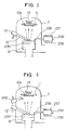
- Fig. 1 is a construction diagram showing an apparatus used for film formation according to an embodiment of the present invention
- Figs. 2, 3 and 4 are construction diagrams showing organic film forming apparatuses capable of controlling the pressure and temperature of a material substance
- Figs. 5A, 5B and 5C are construction diagrams of the material substance blowout outlet of the apparatuses of Figs. 2 through 4;
- Fig. 6 is a construction diagram of a large-area organic film forming apparatus according to an embodiment of the present invention.
- Fig. 7 is a diagram for explaining the operation of Fig. 6;
- Figs. 8, 9 are arrangement diagrams showing a large-area organic film forming apparatus according to another embodiment of the present invention.
- Fig.1 is a diagram showing a construction of an apparatus for forming a fluorine-containing polymer film on an aluminum substrate.
- a gas supply pipe 8 in a vacuum chamber 7, there are provided a gas supply pipe 8, a cooling head 9, a substrate 10a attached to a substrate holder 11, a heater 14 for heating the substrate, an ion source 12, and a laser light generator 233.
- the vacuum chamber 7 is evacuated to about 1.3 ⁇ 10 -5 Pa (1 ⁇ 10 -7 Torr) by vacuum pump (not shown) through an exhaust port 230.
- the cooling head 9 can be cooled to the temperature of liquid nitrogen.
- the laser light generator 233 is a pulse-operated CO 2 laser and outputs a maximum of 1 joule.
- a film forming operation was performed as follows. A mixed gas of CHF 3 and C 2 F 2 was introduced through the gas supply pipe nozzle 8 onto the cooling head 9 cooled to the temperature of liquid nitrogen, where a solidified layer 235 was formed which was used as the target. An argon ion beam 16 of about 6 to 10 eV generated by an ion source 12 was applied to a solidified layer 235 and also, an infrared laser light 234 of a wavelength of 10.6 pm and as much as 0.5 joule was applied to the solidified layer 235, whereby particles (molecules) were sputtered.
- Part of the particles 231 are deposited on a mirror-finished 12.7 cm (5-in.) aluminum substrate (1 mm thick) 10a held at 100°C, thus forming a thin film.
- a film with a thickness 10 nm (100 ⁇ ) was formed for the following evaluation test.
- the laser light 234 was applied to facilitate the production of radicals. Even if the laser light 234 is not applied, a film can be formed, but in that case, the film forming speed decreases.
- the thus formed film was assumed to comprise crosslinked polymers.
- the ratio of the constituent elements was 34.8% C : 12.3% H : 52.6% F.
- the film forming speed was 50 nm/min.
- the aluminum substrate coated with this fluorine-containing polymer film was subjected to a lubrication performance test by a pin-on-disk wear tester. By using a 30-mm diameter spherical sapphire pin, the surface of the specimen was inspected after 20000 revolutions under the condition of 20 g load and 20 m/s peripheral speed. It was confirmed that the lubricating layer had not been damaged, and it became clear that the this film had an excellent lubricating performance. It was also recognized that this film had good corrosion resistance.
- a film was formed by the plasma polymerization method.
- the film obtained was found to be crosslinked three-dimensionally, and it exhibited a good lubricating performance, but had susceptibility to corrosion.
- the film forming speed was about 35 nm/min.
- a film of chainlike crosslinked polymers can be formed on the substrate, and this film shows good sliding performance.
- the film formation in the present invention ensures better corrosion resistance and higher film forming speed than in the conventional plasma polymerization method which uses the same gas mixture.
- Fig. 2 is a diagram showing the construction of a film forming apparatus capable of controlling the pressure and temperature of a material substance.
- an ion source 12 is fitted to a vacuum chamber 7, and in the vacuum chamber 7, there are arranged a substrate 10a attached to a substrate holder 11, a cooling head 9 for forming a solidified layer of a material substance thereon, and a material substance introducing pipe 236 for introducing a material substance which is in gaseous or liquid state at normal temperature and pressure.
- a material substance is supplied into the material substance introducing pipe 236 by a pressure and temperature control section 238.
- the pressure of the material substance can be controlled by changing its flow rate, and the temperature of the material substance can be controlled by operating a cooling plate 237 and a heater 239.
- the apparatus of Fig. 2 operates as follows.
- a material substance comprising an organic compound and controlled at predetermined pressure and temperature, is supplied onto the cooling head 9 through the material substance introducing pipe 236.
- the cooling head 9 is held below the solidifying points of the material substance by a refrigerator (not shown), so that a solidified layer is formed.
- an ion beam of about 10 eV produced in the ion source 12 is applied to the solidified layer 235, particles are sputtered from the solidified layer 235, thus depositing a film of an organic compound on the substrate 10a held at a predetermined temperature.
- the pressure and temperature control section 238 controls the supply (blowout) speed of the gas so as to be less than sonic velocity. If the gas gushes out at a velocity faster than sonic velocity, shock waves occur inside the vacuum chamber 7, producing unfavorable effects on the formation of a film. It became clear that when the gas blowout speed is slower than sonic velocity, the faster the speed, the more quickly the solidified layer 235 is formed. Therefore, in forming a film, it is desirable to set the optimal gas blowout speed to allow compensation - neither excessive nor insufficient - for the decrease in the solidified layer 235 due to sputtering.
- a good film can be formed by raising the temperature of a material substance 5 to 10°C higher than its boiling point and then by lowering the material substance temperature on the cooling head to 5 to 10°C lower than its melting point.
- a material substance the melting point of which is -142.5°C, forms a solidified layer 235.
- an argon ion beam 16 of about 6 to 10 eV to the solidified layer 235 to sputter particles therefrom, a film was formed on the aluminum substrate 10a held at 100°C.
- the film comprised polytetrafluorethylene -CF 2 -CF 2 - n , and that there was no disorder in the chemical composition, which occurred when a film was formed when the temperature of the material substance is room temperature.
- Fig. 3 is a modification of the film forming apparatus capable of controlling the pressure and temperature of a material substance.
- This apparatus is the same as the one shown in Fig. 2, excepting that there is further provided an ion source 240 for irradiation of the substrate 10a.
- an ion source 240 for irradiation of the substrate 10a By using the apparatus of Fig. 3 and tetrafluoroethylene as the material substance, a film was formed on the aluminum substrate 10a. It was confirmed that the film was polytetrafluoroethylene with less disorder in the chemical composition like the film formed by the apparatus of Fig. 2.
- Fig. 4 is another modification of the film forming apparatus capable of controlling the pressure and temperature of a material substance.
- the apparatus in Fig. 4 is almost identical with the one of Fig. 2, with only the exception that the material substance introducing pipe 236 is adapted to be movable above the cooling head 9.
- the solidified layer can be formed with uniform thickness and the thickness distribution of the film formed by sputtering on the substrate 10a can be made uniform.
- Figs. 5A, 5B and 5C show a modification of the material substance blowout nozzle of the material substance introducing pipe 236.
- Fig. 5a shows the nozzle having many holes
- Fig. 5B shows the nozzle widened in a taper form to supply the material in a wide range
- Fig. 5C shows the nozzle which has one or more holes and can pivot.
- a large-area film forming apparatus As shown in Fig. 6, in a vacuum chamber 7, there are arranged an ion source 12, an introducing pipe 3 for introducing into a vacuum a material substance in gaseous or liquid state at normal temperature and pressure, a cooling head 4, a filament 14 for heating a substrate, a substrate holder 11, and a substrate 10a.
- the material substance introducing pipe 3 in a pipe for has a plurality of holes bored at least in a row in the axial direction at the surface of the pipe.
- the substrate 10a is a rectangular prism (thin in thickness) long in a direction perpendicular to the surface of the paper on which there is Fig. 6. As shown in Fig. 6, as shown in Fig.
- the cooling head 4 has a cylindrical form, and it can be cooled to about the temperature of liquid nitrogen and is rotatable about its axis.
- the vacuum chamber 7 is evacuated to 1.3 ⁇ 10 -5 Pa (1 ⁇ 10 -7 Torr) by a vacuum pump (not shown).
- a mixed gas of HCF 3 and C 2 F 6 is introduced into a vacuum through the material substance introducing pipe 3, and a solidified layer of the mixed gas is formed on the surface of the cooling head 4.
- An argon ion beam 16 with energy of about 6 to 10 eV is applied to the solidified layer, and sputtered particles 231 are deposited on the aluminum substrate 10a to form an organic film.
- a CO2 laser light is applied to near the above-mentioned solidified layer to promote the production of radicals, the film forming speed can be improved.
- a film can be formed on a large-area substrate long either in the vertical or horizontal side.
- a substrate 10a has a large area in a generally square shape and is movable in the arrow direction by a substrate feed mechanism 242.
- a solidified layer of a material substance introduced into a vacuum through the material supply pipe 3 is formed on the surface of the cooling head 4, particles are sputtered by an ion beam from the ion source 12 to form a film on the substrate 10a.
- This operation is the same as that by the apparatus of Fig. 6.
- a film is formed while the substrate 10a is moved in the direction of the arrows, making it possible to form an organic film substantially uniform in quality and thickness even on a large-area substrate on which a square film is to be deposited.
- the region in which a solidified layer of material substance is formed can be separated from the region to which an ion beam 16 is applied, so that large quantities of ion beam can be applied and the film forming speed can be increased, accordingly.
- FIG. 9 Yet another example of the large-area film forming apparatus will be described with reference to Fig. 9.
- a vacuum chamber 7 there are provided an ion source 12, a material introducing pipe 3, a cooling head 4, a filament 14 for heating, a substrate 10a, and a substrate feed mechanism 242.
- This arrangement of the parts is the same as in the apparatus in Fig. 8, but only difference is that there are further provided a slit 243 for shaping the sputtered particles and a speed control circuit 245 for changing the feed (moving) speed of the substrate.
- an ion beam 16 is applied to a solidified layer of material substance formed on the surface of the cooling head 4, and a film is formed by depositing sputtered particles 231 by moving the substrate 10a.
- This film forming operation is the same as in the apparatus of Fig. 8.
- the thickness of the film deposited on the substrate 10a can be set arbitrarily by controlling the substrate feed speed by the speed control circuit 245 and using the slit 243.
- ion beams were used for irradiation of the substrate formed on the surface of a target or a cooling head, but other particle beams such as a neutral particle beam or a plasma may be used.
- particle beams such as a neutral particle beam or a plasma
- the same effect can be achieved by using the types of particles other than those of argon.
- the film forming speed differs with the kinds of particles.
Landscapes
- Chemical & Material Sciences (AREA)
- Chemical Kinetics & Catalysis (AREA)
- Engineering & Computer Science (AREA)
- Materials Engineering (AREA)
- Mechanical Engineering (AREA)
- Metallurgy (AREA)
- Organic Chemistry (AREA)
- Physical Vapour Deposition (AREA)
- Physical Deposition Of Substances That Are Components Of Semiconductor Devices (AREA)
Claims (11)
- Verfahren zur Bildung eines Films, mit folgenden Schritten, die in einer Vakuumkammer ausgeführt werden:Halten eines Targets (13, 235) aus einer organischen Verbindung, die bei normaler Temperatur und normalem Druck flüssig oder gasförmig ist, in verfestigter Form bei einer Temperatur unterhalb ihres Schmelzpunktes,Sputtern des Targets unter Verwendung eines Teilchenstrahls (16) mit einer Teilchenenergie, die groß genug ist, inter-molekulare Bindungen aufzubrechen, und nicht groß genug ist, intra-molekulare Bindungen der verfestigten Verbindung aufzubrechen, undHalten eines Substrats (10), so daß darauf Teilchen abgeschieden werden, die durch das Sputtern erzeugt sind, wobei die abgeschiedenen Teilchen den Film bilden.
- Verfahren nach Anspruch 1, wobei die Teilchenenergie etwa 10 eV oder weniger beträgt.
- Verfahren nach Anspruch 1 oder 2, wobei die Verbindung in die Vakuumkammer (7) eingeführt wird und auf einem Targetkopf (9), der unter die Schmelztemperatur der Verbindung gekühlt ist, adsorbiert wird.
- Verfahren nach Anspruch 3, wobei das Einführen der Verbindung während des Sputterns fortdauert, um die adsorbierte Menge der Verbindung konstant zu halten.
- Verfahren nach Anspruch 3 oder 4, mit einem Schritt zum Steuern der Temperatur der eingeführten Verbindung.
- Verfahren nach einem der Ansprüche 1 bis 5, wobei die Verbindung auf einem Targetkopf (4) gehalten wird, der gedreht oder hin- und herbewegt wird.
- Verfahren nach Anspruch 6, wobei der Targetkopf (4) eine zylindrische Form aufweist und gedreht wird, während das Substrat (10a) im wesentlichen parallel zum Targetkopf bewegt wird.
- Verfahren nach einem der Ansprüche 1 bis 7, wobei das Substrat (10a) Wärme oder einem anregenden Strahl mit Ionen, Elektronen, Radikalen und/oder Licht ausgesetzt wird.
- Verfahren nach einem der Ansprüche 1 bis 8, wobei mindestens ein Teil der durch Sputtern erzeugten Teilchen durch eine Einrichtung (233, 234) für Laserlicht oder Elektronenstöße ionisiert wird und der Film gebildet wird, während das Substrat (10a) den ionisierten Teilchen ausgesetzt wird.
- Verfahren nach einem der Ansprüche 1 bis 9, wobei zwei verschiedene Verbindungen, die bei normaler Temperatur und normalem Druck gasförmig oder flüssig sind, in die Vakuumkammer (7) eingeführt werden, ein Targetkopf (9) in der Vakuumkammer auf eine Temperatur unterhalb des Schmelzpunktes jeder der Verbindungen gekühlt wird und auf dem Targetkopf eine Mischung der Verbindungen adsorbiert wird.
- Vorrichtung zur Bildung eines Films in einer Vakuumkammer (7), aufweisend:einen Targetkopf (9) zum Halten eines Targets (13, 235) aus einer organischen Verbindung, die bei normaler Temperatur und normalem Druck flüssig oder gasförmig ist, in verfestigter Form bei einer Temperatur unterhalb ihres Schmelzpunktes,eine Einrichtung (12) zum Sputtern des Targets durch Verwenden eines Teilchenstrahls (16) mit einer Teilchenenergie, die hoch genug ist, inter-molekulare kristalline Bindungen aufzubrechen, jedoch nicht hoch genug ist, intra-molekulare Bindungen der verfestigten Verbindung aufzubrechen, undeinen Halter (11) zum Halten eines Substrats (10), so daß darauf Teilchen (231), die durch das Sputtern erzeugt werden, abgeschieden werden, wobei die abgeschiedenen Teilchen den Film bilden.
Applications Claiming Priority (6)
| Application Number | Priority Date | Filing Date | Title |
|---|---|---|---|
| JP3359489A JPH07116596B2 (ja) | 1989-02-15 | 1989-02-15 | 薄膜形成方法、及びその装置 |
| JP3359489 | 1989-02-15 | ||
| JP33594/89 | 1989-02-15 | ||
| JP15678789 | 1989-06-21 | ||
| JP15678789A JPH0611912B2 (ja) | 1989-06-21 | 1989-06-21 | 有機薄膜形成方法、及びその装置並びに粒子線発生器 |
| JP156787/89 | 1989-06-21 |
Publications (3)
| Publication Number | Publication Date |
|---|---|
| EP0383301A2 EP0383301A2 (de) | 1990-08-22 |
| EP0383301A3 EP0383301A3 (de) | 1991-11-21 |
| EP0383301B1 true EP0383301B1 (de) | 1999-09-15 |
Family
ID=26372317
Family Applications (1)
| Application Number | Title | Priority Date | Filing Date |
|---|---|---|---|
| EP90102897A Expired - Lifetime EP0383301B1 (de) | 1989-02-15 | 1990-02-14 | Verfahren und Vorrichtung zur Bildung eines Films |
Country Status (4)
| Country | Link |
|---|---|
| US (1) | US5064520A (de) |
| EP (1) | EP0383301B1 (de) |
| KR (1) | KR900013591A (de) |
| DE (1) | DE69033286T2 (de) |
Families Citing this family (48)
| Publication number | Priority date | Publication date | Assignee | Title |
|---|---|---|---|---|
| US5837332A (en) * | 1989-11-19 | 1998-11-17 | Nihon Victor Kabushiki-Kaisha | Method and apparatus for preparing crystal thin films by using a surface acoustic wave |
| EP0508478B1 (de) * | 1991-04-12 | 1996-07-03 | Nissin Electric Company, Limited | Verfahren zur Erzeugung eines Metallfilms sowie durch einen Aluminiumfilm beschichtetes Erzeugnis |
| US5211824A (en) * | 1991-10-31 | 1993-05-18 | Siemens Solar Industries L.P. | Method and apparatus for sputtering of a liquid |
| US5240583A (en) * | 1992-01-14 | 1993-08-31 | Honeywell Inc. | Apparatus to deposit multilayer films |
| FR2691144B1 (fr) * | 1992-05-13 | 1994-10-14 | Alcatel Nv | Procédé d'élaboration d'une préforme pour fibre optique. |
| BE1006967A3 (fr) * | 1993-04-16 | 1995-02-07 | Cockerill Rech & Dev | Procede pour la formation d'un revetement sur un substrat par pulverisation cathodique reactive. |
| US5432313A (en) * | 1993-06-23 | 1995-07-11 | The United States Of America As Represented By The Secretary Of The Army | Target configurations for increasing the size of films prepared by laser ablation |
| DE4427215A1 (de) * | 1993-08-02 | 1995-02-23 | Agency Ind Science Techn | Transparente und leitfähige ultradünne Filme und Verfahren zu ihrer Herstellung |
| US5429732A (en) * | 1994-02-14 | 1995-07-04 | Hughes Aircraft Company | High rate ion beam sputtering process |
| JPH08136932A (ja) * | 1994-11-08 | 1996-05-31 | Seiko Instr Inc | 液晶に微少に傾斜した垂直配列を導入する方法、液晶電気光学素子及び液晶ライトバルブ |
| JP3523405B2 (ja) * | 1996-01-26 | 2004-04-26 | 株式会社日立製作所 | 荷電ビーム処理によるパターン形成方法及び荷電ビーム処理装置 |
| US5667645A (en) * | 1996-06-28 | 1997-09-16 | Micron Technology, Inc. | Method of sputter deposition |
| TW335504B (en) * | 1996-07-09 | 1998-07-01 | Applied Materials Inc | A method for providing full-face high density plasma deposition |
| US5985033A (en) * | 1997-07-11 | 1999-11-16 | Applied Materials, Inc. | Apparatus and method for delivering a gas |
| WO2000022184A1 (en) * | 1998-10-12 | 2000-04-20 | The Regents Of The University Of California | Laser deposition of thin films |
| US6265722B1 (en) | 1999-08-31 | 2001-07-24 | Micron Technology, Inc. | Organic field ionization source |
| DE60135100D1 (de) * | 2000-03-24 | 2008-09-11 | Cymbet Corp | E mit ultradünnem elektrolyten |
| US20070281109A1 (en) * | 2000-03-31 | 2007-12-06 | Carl Zeiss Smt Ag | Multilayer system with protecting layer system and production method |
| US6580053B1 (en) * | 2000-08-31 | 2003-06-17 | Sharp Laboratories Of America, Inc. | Apparatus to control the amount of oxygen incorporated into polycrystalline silicon film during excimer laser processing of silicon films |
| US6610363B2 (en) | 2000-10-18 | 2003-08-26 | Nanofilm, Ltd. | Composition with film forming alkylsilsesquioxane polymer and method for applying hydrophobic films to surfaces |
| US6890987B2 (en) * | 2000-10-18 | 2005-05-10 | Nanofilm, Ltd. | Product for vapor deposition of films of amphiphilic molecules or polymers |
| US6402904B1 (en) * | 2001-03-16 | 2002-06-11 | 4 Wave, Inc. | System and method for performing sputter deposition using independent ion and electron sources and a target biased with an a-symmetric bi-polar DC pulse signal |
| US6679976B2 (en) | 2001-03-16 | 2004-01-20 | 4Wave, Inc. | System and method for performing sputter deposition with multiple targets using independent ion and electron sources and independent target biasing with DC pulse signals |
| US20040198898A1 (en) * | 2001-08-03 | 2004-10-07 | Arora Pramod K. | Method for vapor deposition of hydrophobic films on surfaces |
| JP3971603B2 (ja) * | 2001-12-04 | 2007-09-05 | キヤノンアネルバ株式会社 | 絶縁膜エッチング装置及び絶縁膜エッチング方法 |
| JP3910466B2 (ja) * | 2002-02-26 | 2007-04-25 | 独立行政法人科学技術振興機構 | 半導体又は絶縁体/金属・層状複合クラスタの作製方法及び製造装置 |
| US6719936B2 (en) * | 2002-08-23 | 2004-04-13 | Eastman Kodak Company | Method of making a solid compacted pellet of organic material for vacuum deposition of OLED displays |
| US6906436B2 (en) * | 2003-01-02 | 2005-06-14 | Cymbet Corporation | Solid state activity-activated battery device and method |
| US7294209B2 (en) | 2003-01-02 | 2007-11-13 | Cymbet Corporation | Apparatus and method for depositing material onto a substrate using a roll-to-roll mask |
| US7603144B2 (en) | 2003-01-02 | 2009-10-13 | Cymbet Corporation | Active wireless tagging system on peel and stick substrate |
| US7211351B2 (en) | 2003-10-16 | 2007-05-01 | Cymbet Corporation | Lithium/air batteries with LiPON as separator and protective barrier and method |
| JP2007518246A (ja) | 2004-01-06 | 2007-07-05 | シンベット コーポーレーション | 境界を有する1若しくはそれ以上の層を備える層状のバリア構造及び該バリア構造の製造方法 |
| US7216544B2 (en) * | 2005-03-25 | 2007-05-15 | The Boeing Company | Ultrasonic inspection reference standard for composite Materials |
| KR101387855B1 (ko) | 2005-07-15 | 2014-04-22 | 사임베트 코퍼레이션 | 연질 및 경질 전해질층을 가진 박막 배터리 및 그 제조방법 |
| US7776478B2 (en) | 2005-07-15 | 2010-08-17 | Cymbet Corporation | Thin-film batteries with polymer and LiPON electrolyte layers and method |
| KR100699858B1 (ko) * | 2005-08-03 | 2007-03-27 | 삼성전자주식회사 | 극자외선 리소그래피용 반사 디바이스 및 그 제조 방법 및이를 적용한 극자외선 리소그래피용 마스크, 프로젝션광학계 및 리소그래피 장치 |
| US8835880B2 (en) * | 2006-10-31 | 2014-09-16 | Fei Company | Charged particle-beam processing using a cluster source |
| JP2009015910A (ja) * | 2007-06-29 | 2009-01-22 | Toshiba Corp | 電子線描画方法 |
| WO2009118034A1 (de) * | 2008-03-27 | 2009-10-01 | Fraunhofer-Gesellschaft zur Förderung der angewandten Forschung e.V. | Verfahren zur herstellung eines mehrkomponentigen, polymer- und metallhaltigen schichtsystems, vorrichtung und beschichteter gegenstand |
| MX346377B (es) * | 2011-04-20 | 2017-03-16 | Oerlikon Surface Solutions Ag Pfäffikon | Método para proporcionar impulsos de potencia secuenciales. |
| US11527774B2 (en) | 2011-06-29 | 2022-12-13 | Space Charge, LLC | Electrochemical energy storage devices |
| US9853325B2 (en) | 2011-06-29 | 2017-12-26 | Space Charge, LLC | Rugged, gel-free, lithium-free, high energy density solid-state electrochemical energy storage devices |
| US10658705B2 (en) | 2018-03-07 | 2020-05-19 | Space Charge, LLC | Thin-film solid-state energy storage devices |
| US10601074B2 (en) | 2011-06-29 | 2020-03-24 | Space Charge, LLC | Rugged, gel-free, lithium-free, high energy density solid-state electrochemical energy storage devices |
| US11996517B2 (en) | 2011-06-29 | 2024-05-28 | Space Charge, LLC | Electrochemical energy storage devices |
| CA3015805A1 (en) * | 2017-08-28 | 2019-02-28 | Institut National De La Recherche Scientifique | Method and system for fabrication of crystals using laser-accelerated particle beams or secondary sources |
| JP7145031B2 (ja) * | 2017-12-25 | 2022-09-30 | 東京エレクトロン株式会社 | 基板を処理する方法、プラズマ処理装置、及び基板処理装置 |
| CN111934101B (zh) * | 2020-07-31 | 2022-11-25 | 国家纳米科学中心 | 一种激发二维范德华材料极化激元的方法 |
Family Cites Families (9)
| Publication number | Priority date | Publication date | Assignee | Title |
|---|---|---|---|---|
| US3492215A (en) * | 1967-02-27 | 1970-01-27 | Bendix Corp | Sputtering of material simultaneously evaporated onto the target |
| US4381453A (en) * | 1980-12-31 | 1983-04-26 | International Business Machines Corporation | System and method for deflecting and focusing a broad ion beam |
| US4416755A (en) * | 1981-04-03 | 1983-11-22 | Xerox Corporation | Apparatus and method for producing semiconducting films |
| JPS6044A (ja) * | 1983-06-16 | 1985-01-05 | Hitachi Ltd | 二次イオン化質量分析装置 |
| US4637869A (en) * | 1984-09-04 | 1987-01-20 | The Standard Oil Company | Dual ion beam deposition of amorphous semiconductor films |
| US4664769A (en) * | 1985-10-28 | 1987-05-12 | International Business Machines Corporation | Photoelectric enhanced plasma glow discharge system and method including radiation means |
| US4793908A (en) * | 1986-12-29 | 1988-12-27 | Rockwell International Corporation | Multiple ion source method and apparatus for fabricating multilayer optical films |
| JP2555045B2 (ja) * | 1987-01-19 | 1996-11-20 | 株式会社日立製作所 | 薄膜形成方法及びその装置 |
| JP3610999B2 (ja) | 1996-06-07 | 2005-01-19 | 松下電器産業株式会社 | 半導体素子の実装方法 |
-
1990
- 1990-02-14 DE DE69033286T patent/DE69033286T2/de not_active Expired - Fee Related
- 1990-02-14 US US07/480,131 patent/US5064520A/en not_active Expired - Fee Related
- 1990-02-14 EP EP90102897A patent/EP0383301B1/de not_active Expired - Lifetime
- 1990-02-15 KR KR1019900001831A patent/KR900013591A/ko not_active Ceased
Non-Patent Citations (1)
| Title |
|---|
| argon during ion bombardment" * |
Also Published As
| Publication number | Publication date |
|---|---|
| KR900013591A (ko) | 1990-09-06 |
| DE69033286T2 (de) | 2000-05-25 |
| EP0383301A3 (de) | 1991-11-21 |
| US5064520A (en) | 1991-11-12 |
| DE69033286D1 (de) | 1999-10-21 |
| EP0383301A2 (de) | 1990-08-22 |
Similar Documents
| Publication | Publication Date | Title |
|---|---|---|
| US5064520A (en) | Method and apparatus for forming a film | |
| CA1140078A (en) | Method and apparatus for pretreating and depositing thin films on substrates | |
| US8273407B2 (en) | Systems and methods for forming magnetic nanocomposite materials | |
| JPS62183023A (ja) | 磁気記録媒体 | |
| JPH0333778B2 (de) | ||
| US4584078A (en) | Method of producing fine particles | |
| EP0508478B1 (de) | Verfahren zur Erzeugung eines Metallfilms sowie durch einen Aluminiumfilm beschichtetes Erzeugnis | |
| US6146505A (en) | Sputtering method for producing layered aluminium fine particles and use thereof | |
| US4925700A (en) | Process for fabricating high density disc storage device | |
| EP1008670B1 (de) | Ein Verfahren zur Herstellung eines Sputtertargets | |
| Cheng et al. | Substrate bias dependence of the structure and internal stress of TiN films deposited by the filtered cathodic vacuum arc | |
| JP2697753B2 (ja) | 直流グロー放電による金属被膜の堆積法 | |
| Hagemeyer et al. | Crystallographic texture and morphology of obliquely deposited Co-Cr magnetic thin films on flexible polymeric substrates | |
| JPH03174307A (ja) | 酸化物超電導体の製造方法 | |
| JPH0324262A (ja) | 有機薄膜形成方法、及びその装置並びに粒子線発生器 | |
| Mašek et al. | RHEED investigation of lattice deformations of α-Al2O3 supported Pd particles | |
| Hu et al. | Gold clusters deposited on highly oriented pyrolytic graphite by pulse laser ablation and liquid metal ion source | |
| Glocker et al. | Ion beam sputter deposition onto levitated and stalk mounted laser fusion targets | |
| Ishii et al. | A new process for producing a granular material | |
| Rigsbee | Plasma-and ion-beam assisted physical vapor deposition: processes and materials | |
| Niyamakom | Influence of deposition parameters on morphology, growth and structure of crystalline and amorphous organic thin films:(the case of perylene and α-NPD [alpha-NPD]) | |
| JP4527126B2 (ja) | 光ディスク保護膜形成用スパッタリングターゲット | |
| WO1998015668A1 (en) | Production method of laminate body, and the laminate body | |
| JP2703359B2 (ja) | 磁気記録媒体及びその製造方法 | |
| RIGSBEE | PLASMA-AND ION-BEAM ASSISTED PHYSICAL VAPOR DEPOSITION: PROCESSES AND MATERIALS J. M. RIGSBEE |
Legal Events
| Date | Code | Title | Description |
|---|---|---|---|
| PUAI | Public reference made under article 153(3) epc to a published international application that has entered the european phase |
Free format text: ORIGINAL CODE: 0009012 |
|
| AK | Designated contracting states |
Kind code of ref document: A2 Designated state(s): DE FR GB |
|
| 17P | Request for examination filed |
Effective date: 19901220 |
|
| PUAL | Search report despatched |
Free format text: ORIGINAL CODE: 0009013 |
|
| AK | Designated contracting states |
Kind code of ref document: A3 Designated state(s): DE FR GB |
|
| 17Q | First examination report despatched |
Effective date: 19930723 |
|
| GRAG | Despatch of communication of intention to grant |
Free format text: ORIGINAL CODE: EPIDOS AGRA |
|
| GRAG | Despatch of communication of intention to grant |
Free format text: ORIGINAL CODE: EPIDOS AGRA |
|
| GRAH | Despatch of communication of intention to grant a patent |
Free format text: ORIGINAL CODE: EPIDOS IGRA |
|
| GRAH | Despatch of communication of intention to grant a patent |
Free format text: ORIGINAL CODE: EPIDOS IGRA |
|
| GRAA | (expected) grant |
Free format text: ORIGINAL CODE: 0009210 |
|
| AK | Designated contracting states |
Kind code of ref document: B1 Designated state(s): DE FR GB |
|
| REF | Corresponds to: |
Ref document number: 69033286 Country of ref document: DE Date of ref document: 19991021 |
|
| PGFP | Annual fee paid to national office [announced via postgrant information from national office to epo] |
Ref country code: FR Payment date: 19991215 Year of fee payment: 11 |
|
| ET | Fr: translation filed | ||
| PGFP | Annual fee paid to national office [announced via postgrant information from national office to epo] |
Ref country code: DE Payment date: 19991223 Year of fee payment: 11 |
|
| PGFP | Annual fee paid to national office [announced via postgrant information from national office to epo] |
Ref country code: GB Payment date: 20000204 Year of fee payment: 11 |
|
| PLBE | No opposition filed within time limit |
Free format text: ORIGINAL CODE: 0009261 |
|
| STAA | Information on the status of an ep patent application or granted ep patent |
Free format text: STATUS: NO OPPOSITION FILED WITHIN TIME LIMIT |
|
| 26N | No opposition filed | ||
| PG25 | Lapsed in a contracting state [announced via postgrant information from national office to epo] |
Ref country code: GB Free format text: LAPSE BECAUSE OF NON-PAYMENT OF DUE FEES Effective date: 20010214 |
|
| GBPC | Gb: european patent ceased through non-payment of renewal fee |
Effective date: 20010214 |
|
| PG25 | Lapsed in a contracting state [announced via postgrant information from national office to epo] |
Ref country code: FR Free format text: LAPSE BECAUSE OF NON-PAYMENT OF DUE FEES Effective date: 20011031 |
|
| REG | Reference to a national code |
Ref country code: FR Ref legal event code: ST |
|
| PG25 | Lapsed in a contracting state [announced via postgrant information from national office to epo] |
Ref country code: DE Free format text: LAPSE BECAUSE OF NON-PAYMENT OF DUE FEES Effective date: 20011201 |