EP0383610B1 - Verfahren zum Herstellen einer Halbleitervorrichtung - Google Patents
Verfahren zum Herstellen einer Halbleitervorrichtung Download PDFInfo
- Publication number
- EP0383610B1 EP0383610B1 EP90301674A EP90301674A EP0383610B1 EP 0383610 B1 EP0383610 B1 EP 0383610B1 EP 90301674 A EP90301674 A EP 90301674A EP 90301674 A EP90301674 A EP 90301674A EP 0383610 B1 EP0383610 B1 EP 0383610B1
- Authority
- EP
- European Patent Office
- Prior art keywords
- forming
- recess
- insulator film
- wiring layer
- film
- Prior art date
- Legal status (The legal status is an assumption and is not a legal conclusion. Google has not performed a legal analysis and makes no representation as to the accuracy of the status listed.)
- Expired - Lifetime
Links
Images



Classifications
-
- H—ELECTRICITY
- H10—SEMICONDUCTOR DEVICES; ELECTRIC SOLID-STATE DEVICES NOT OTHERWISE PROVIDED FOR
- H10W—GENERIC PACKAGES, INTERCONNECTIONS, CONNECTORS OR OTHER CONSTRUCTIONAL DETAILS OF DEVICES COVERED BY CLASS H10
- H10W20/00—Interconnections in chips, wafers or substrates
- H10W20/01—Manufacture or treatment
- H10W20/071—Manufacture or treatment of dielectric parts thereof
- H10W20/081—Manufacture or treatment of dielectric parts thereof by forming openings in the dielectric parts
-
- H—ELECTRICITY
- H10—SEMICONDUCTOR DEVICES; ELECTRIC SOLID-STATE DEVICES NOT OTHERWISE PROVIDED FOR
- H10W—GENERIC PACKAGES, INTERCONNECTIONS, CONNECTORS OR OTHER CONSTRUCTIONAL DETAILS OF DEVICES COVERED BY CLASS H10
- H10W20/00—Interconnections in chips, wafers or substrates
- H10W20/40—Interconnections external to wafers or substrates, e.g. back-end-of-line [BEOL] metallisations or vias connecting to gate electrodes
Definitions
- the present invention relates to a manufacturing method of semiconductor device having fine contacts.
- a selective oxidation (LOCOS) film 2 for separation among elements is formed in a specified region in a thickness of about 500 nm. Consequently, a gate oxide film 3 of 20 nm in thickness is formed on the principal plane of the silicon substrate 1.
- a polycrystalline silicon gate layer 4a of 300 to 500 nm in thickness and a polycrystalline silicon wiring layer 4b are formed on the gate oxide film 3 and the oxidation film 2 respectively.
- ions are implanted to form a diffusion layer (diffusion layer wiring) 5, and ions are activated by annealing, thereby forming a MOS type semiconductor device.
- an oxide film 6 of about 300 nm in thickness is deposited on the whole area of the substrate surface [Fig. 5 (a)].
- the oxide film 6 is generally formed by the chemical vapor deposition (CVD) method.
- a BPSG film 7 of 400 nm in thickness is deposited by CVD.
- the BPSG film 7 has impurity concentrations of, for example, 3 wt.% of boron (B) and 5 wt.% of phosphorus (P), approximately.
- heat treatment is applied for 60 minutes at 900°C to flow the BPSG film 7 in order to lessen the step difference of the surface of the BPSG film [Fig. 5 (b)].
- the oxide film 6 prevents thermal diffusion of phosphorus (P) and boron (B) from the BPSG film 7 to the silicon substrate 1.
- a photoresist (not shown) is applied, a specified resist pattern is formed by photoetching, and using this resist pattern as the mask, the oxide film 6 and BPSG film 7 are removed by etching, thereby forming contact hole 8. Furthermore, the resist pattern is removed [Fig. 5 (c)].
- a polycide wiring layer 9 is formed on the BPSG film 7 and in the contact hole 8 [Fig. 5 (d)].
- This polycide wiring layer 9 is composed of two layers, that is, the lower layer of 200 nm thick polycrystalline silicon film 9a and the upper layer of 200 nm thick tungsten silicide (WSix) film 9b. Since phosphorus is to be introduced into the polycrystalline silicon film 9a, it is heat-treated in a nitrogen atmosphere containing phosphorus compound, and the tungsten silicide film 9b is deposited by CVD.
- This polycide wiring layer 9 is patterned by anisotropic etching, such as RIE.
- This polycide wiring layer 9 has lower wiring resistance than the single layer of polycrystalline silicon, so that the circuit delay due to the wiring resistance may be improved.
- a BPSG film 10 is deposited in a thickness of 500 nm.
- the BPSG film 10 has impurity concentrations of, for example, 3 wt.% of boron (B) and 5 wt.% of phosphorus (P), approximately.
- heat treatment is performed for 60 minutes at 900°C to flow the BPSG film 10, thereby lessening the step difference due to the polycrystalline silicon gate layer 4a, 4b and the polycide wiring layer 9.
- a photoresist (not shown) is applied, and a specified resist pattern is formed by photoetching.
- the oxide film 6 and BPSG films 7, 10 are removed by RIE etching, and thereby, contact holes 11 are formed [Fig. 5 (e)]. After that, the resist pattern is removed.
- the aluminum alloy wiring layer 12 is deposited in a film thickness of 0.8 ⁇ m in thickness by a known method such as sputtering, and is patterned by anisotropic etching such as RIE etching [Fig. 5 (f)].
- the aspect ratio (hole depth/hole width) of the contact holes 11 becomes high, exceeding 1.
- the aluminum alloy film 12 formed on the side wall of the contact hole 11 becomes thin partly, and the resistance of the aluminum alloy film 12 may increase, the reliability of the aluminum alloy film 12 may be lessened (for example, electromigration may be likely to occur) and other defects may take place.
- electromigration may be likely to occur
- Patent Abstracts of Japan, Volume 13, no. 86 (E-720) (3434) of Japanese Patent Application JP-A-63265431 discloses a semiconductor device having a nitride film for preventing diffusion of an impurity from a BPSG film into a substrate, the nitride film being deposited under the BPSG film.
- United States Patent US-A-4,502,209 discloses a method of forming low resistance contact to silicon, comprising a single processing step of annealing a titanium-rich carbide film deposited on silicon, whereby to produce a stable titanium silicide contact and a stable titanium carbide diffusion barrier between the silicide and a subsequently formed overlying layer of aluminium.
- Patent Abstracts of Japan, volume 9, no. 43 (E-298) (1766) of Japanese Patent Application JP-A-59184548 discloses a method of manufacturing a semiconductor device wherein the diameters of contact holes through two insulation layers to source or drain regions are made to be wider in the second-deposited insulation layer than in the first by using a higher etching speed when etching the second insulation layer than when etching the first.
- the invention in short, is intended to open contact holes of small opening width in the bottom of a recess with a large opening width by forming this recess in the contact hole forming position of an insulator film in advance before opening the contact holes in the insulator film.
- the opening size of the recess above the contact holes may be larger, and by decreasing the shadowing effect, the state of covering of the wiring layer on the side wall of the contact holes is improved, so that decrease of the wiring resistance and enhancement of reliability of the wiring may be achieved.
- the contact holes may be opened at high precision in the bottom of the recesses, it is possible to keep a proper clearance between the contact holes and gate electrodes, even if the semiconductor elements are integrated at high density, and electric leak between wiring layers may be effectively prevented.
- a thermal oxide film is formed on one principal plane of a P-type (100) silicon substrate 21, and a nitride film is deposited on the thermal oxide film.
- a photoresist is applied, exposed and developed, and a window is opened in a region for forming a selective oxide film (LOCOS film) for separation of elements.
- LOC film selective oxide film
- the nitride film is etched, and the thermal oxide film is etched and removed, and the surface of the silicon substrate 21 is exposed. Removing this photoresist, the exposed silicon substrate 21 is oxidized in an oxidizing atmosphere, and a selective oxide film 22 of about 500 nm in thickness is formed.
- the nitride film and thermal oxide film are removed.
- a gate oxide film 23 of 20 nm in thickness a polycrystalline silicon layer 24a and 24b of 300 to 500 nm in thickness is formed by CVD on the oxide film 23 and the selective oxide film 22 respectively.
- the polycrystalline silicon layer 24a is used as a gate electrode, and the polycrystalline silicon layer 24b is used as a wiring layer. This polycrystalline silicon is doped with impurities in order to lower the resistance.
- the impurities are implanted by ion implantation, the impurities are diffused from the vapor phase of the impurity gas, or polycrystalline silicon containing impurities is formed simultaneously with growth by mixing gas containing impurity elements to the gas for growing the polycrystalline silicon by a CVD apparatus for fabricating polycrystalline silicon.
- the polycrystalline silicon is etched, and a polycrystalline silicon gate layer 24a and polycrystalline silicon wiring layer 24b are formed. Ions are then implanted into the whole area of the silicon substrate 21 to form a diffusion layer (diffusion layer wiring) 25. At this time, ions are not implanted into the silicon substrate 21 just beneath the polycrystalline silicon gate layer 24a and the selective oxide film 22 because they serve as masks.
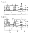
- an oxide film 26 of 300 nm in thickness is deposited on the entire surface of the silicon substrate 21 by CVD [Fig. 1 (a)].
- a BPSG film 27 of 500 nm in thickness is deposited on the oxide film 26 by CVD.
- This BPSG film 27 is composed of an oxide film with, for example, boron concentration of 3 wt.% and phosphorus concentration of 5 wt.%.
- the melting temperature of the BPSG film 27 is lowered, so that it is possible to flow at low temperature.
- the boron concentration is too high, the moisture absorption of the BPSG film 27 increases, and the film composition becomes unstable.
- the phosphorus concentration is too high, the aluminum alloy wiring may corrode.
- boron and phosphorus in the BPSG film 27 diffuse in the oxide film 26, but will not penetrate into the silicon substrate 21 because of the oxide film 26 formed on the silicon substrate in the thickness of about 300 nm in the process of Fig. 1 (a).
- a photoresist is applied, exposed and developed, and a window is opened at a position to be used as contact of the MOS type semiconductor device.
- the BPSG film 27 is dry-etched and removed, and the oxide film 26 is dry-etched, and further beneath the gate oxide film 23 is dry-etched, until the silicon substrate 21 is exposed.
- Dry etching of the BPSG film 27 at this time was conducted by usign a parallel flat plate plasma etching apparatus, using gases of CHF 3 , He, O 2 at the volume rate of 4:15:1, at the total gas flow rate of 100 cc/min, RF electric power of 500 W, for etching time of 120 seconds.
- the high energy ions generated by this dry etching collide against the silicon substrate 21, and the defects may be formed in the exposed surface region of the silicon substrate 21.
- the exposed surface of the silicon substrate 21 is washed, and the spontaneous oxide film formed on the exposed surface of the silicon substrate 21 is removed in the subsequent process, so that the defects in the surface region of the silicon substrate 21 caused by the dry etching are removed.
- buffered hydrofluoric solution mixture of hydrogen fluoride and ammonium fluoride
- a polycrystalline silicon film 29a is deposited on the entire surface of the BPSG film 27 in a thickness of, for exmaple, 200 nm, by CVD to cover the contact hole 28.
- This polycrystalline silicon film 29a is doped with impurities, same as the gate electrode, and, in this case, after growing a non-doped polycrystalline silicon film, heat treatment is conducted for 30 minutes at 900°C in a gas atmosphere of, for example, PH 3 (phospine).
- PH 3 phospine
- the forming condition of the polycrystalline silicon film 29a is the SiH 4 (silane) gas flow rate of 150 cc/min, growth temperature of 600°C, and growth time of 50 minutes.
- tungsten silicide (WSix) film 29b is deposited in a thickness of, for exmaple, 200 nm on the surface of the polycrystalline silicon film 29a.
- the tungsten silicide film 29a is formed by CVD.
- the tungsten silicide film 29b and the lower polycrystalline silicon film 29a are etched and removed by reactive ion etching.
- the etching condition of the tungsten silicide film 29b and the polycrystalline silicon film 29a at this time is, by using the parallel flat plate plasma etching apparatus, the mixing ratio of SF 6 and C 2 Cl 2 F of 1:1, total gas flow rate of 50 cc/min, RF electric power of 100 W, and etching time of 2 minutes.
- a polycide wiring layer 29 comprising the laminate films of polycrystalline silicon film 29a and tungsten silicide film 29b.
- the polycide wiring layer 29 has lower wiring resistance as compared with the polycrystalline silicon single layer, the circuit delay caused by the wiring ressitance may be improved.
- a BPSG film 30 is deposited on the entire surface of the BPSG film 27 and the polycide wiring layer 29 by CVD.
- the impurity concentrations and forming conditions were same as those of the BPSG film 27 shown in Fig. 1 (b), but the film thickness was 300 nm because the step difference on the BPSG film 27 before deposition of the BPSG film 30 is smaller than that on the oxide film 26 shown in Fig. 1 (b).
- a photoresist 31 is applied, exposed and developed, and a window is opened at the position to be used as the contact of the MOS semiconductor device.
- the BPSG film 30 is removed by dry etching, and the BPSG film 27 formed previously in Fig. 1 (b) is also dry-etched.
- the conditions of dry etching of the BPSG film 30 and BPSG film 27 were, by using the parallel flat plate type plasma etching apparatus, the gas mixing ratio of CHF 3 , He, O 2 of 4:5:1, the total gas flow rate of 100 cc/min, RF electric power of 500 W, and etching time of 40 seconds.
- the etching time is carefully controlled, and by such careful controlling, the bottom thickness of the recess 32 can be formed at fluctuations of about ⁇ 10%.
- the recess 32 can be formed by ordinary dry etching, stably, in a highly reliable process.
- the thickness of the residual film of the BPSG film 27 and oxide film 26 beneath the recess 32 is excessive, the effect for improvement of the degree of covering of the step difference of the aluminum alloy to be used as wiring which is formed in the subsequence step is decreased, and hence it is important to employ a stable and highly reliable dry etching process so as to leave the film of an appropriate thickness beneath the recess 32.
- the polycide wiring layer 29 runs transverse in the recess 32. Therefore, when an aluminum alloy wiring layer 36 formed on the side wall of the recess 32 in the subsequent process is connected to the polycide wiring layer 29, the side wall of the polycide wiring layer 29 becomes a step difference, and the degree of covering of the step difference of the aluminum alloy wiring layer 36 is impaired. It is accordingly necessary to consider the forming position of the window of resist pattern 31 so that the recess 32 may not be formed in such a region as to envelope the polycide wiring layer 29 completely.
- the polycide wiring layer 29 is not completely included when the aluminum alloy wiring layer 36 is connected to the diffusion layer 25. Therefore, even in a small wiring gap, a recess 32 having a large window width may be formed.
- the window width of the recess 32 is preferably about 3 ⁇ m, and if too small, the side wall of the recess 32 is steep, and the improvement of the covering of the step difference when the aluminum alloy wiring film is formed in a subsequent process decreases. If too large, to the contrary, the polycide wiring layer 29 runs transverse in the recess 32, and the side wall of the polycide wiring layer 29 becomes steep, and hence the covering of the step difference of aluminum alloy wiring layer is also poor. Therefore, at least, it should be about 1.5 ⁇ m, and at most, it should be about 5 ⁇ m.
- a BPSG film 33 is deposited again on the BPSG film 30 and the whole surface of the recess 32 in a thickness of about 400 nm by CVD.
- the impurity concentrations of the BPSG film 33 are 4 wt.% of boron and 5wt.% of phosphorus.
- the boron concentration of this BPSG film 33 is higher than that of the previous two BPSG films 27, 30, which is because, as stated above, when the concentrations of boron and phosphorus are increased, the melting temperature of the BPSG film 33 is lowered so as to be able to flow at low temperature. However, if the boron concentration is too high, the moisture absorption of the BPSG film 33 increases, and the composition of the film becomes unstable.
- the height from the surface of the BPSG film 27 to the surface of the upper BPSG film 33, that is, the depth of the recess 32 is about 400 to 500 nm, and therefore the boron concentration is increased so that the deposited BPSG film 33 may be favorable in the covering of step diffference, sufficient in flow, and smooth in the shape at the step difference portion.
- the thickness of the BPSG film 33 in this process is determined in consideration that the effect on the improvement of the covering of the step difference of the aluminum alloy film used as the wiring to be formed in the subsequent process may decrease if the thickness of the remaining film in the recess 32 is excessive.
- the BPSG film 27 is caused to flow to flatten the substrate surface [Fig. 1 (g)].
- step difference of the recess 32 and step difference due to wiring are sufficiently lessened, and breakage of aluminum alloy wiring or formation of bridge (electrical short circuit) in the subsequent process can be prevented.
- the contact hole may be opened in the next process.
- the oxide film 26 and gate oxide film 23 are completely removed, when the BPSG film 33 is directly formed on the silicon substrate 21, impurities may diffuse in the silicon substrate 21 due to heat treatment at the time of flow of the BPSG film 33, and therefore it is not recommended to remove the oxide film 26 or gate oxide film 23 on the recess 32.
- a photoresist 34 is applied, exposed and developed, and a patterned photoresist 34 is formed [Fig. 1 (h)].
- This photoresist 34 is formed inside the recess 32, and is set so as to be smaller than the opening width of the recess 32 in which the BPSG film 33 is formed, but the same effects will not be obtained only when smaller than the opening width.
- FIG. 2 an enlarged sectional view of the region of circle A in Fig. 1 (h) is shown in Fig. 2.
- the symbol “L” denotes the pattern width when the width of the photoresist pattern 34 is broad
- “1” is the pattern width when it is narrow
- “H” is the height of the side wall of the contact hole when the pattern width is "L”
- “h” is the height of the side wall of the contact hole when it is "l”.
- the side wall of the BPSG film 33 may be slightly cut off, and when etched by using such photoresist pattern 34, the actual height of the contact portion will be H.
- the height from the surface of the silicon substrate 21 to the BPSG film 33 is about 500 nm, and in this example, the height is more than 500 nm, and the covering of the step difference of the aluminum alloy wiring layer in the subsequent process becomes poor. Further, it becomes difficult to maintain an appropriate gap between the contact hole formed by the photoresist pattern 34 and the polycrystalline silicon gate layer 24a, and thereby, the shrinkage of the semiconductor device becomes difficult.
- the photoresist 34 on the BPSG film 33 is too narrow (width "l” in Fig. 2), the photoresist 34 is formed in the flat portion of the bottom of the BPSG film 33, and the height "h” at this time is equal to the height from the surface of the silicon substrate 21 to the BPSG film 33, being about 500 nm.
- the pattern width "l" of the photoresist 34 is small, as the value of "l" becomes smaller, the aspect ratio in the contact hole becomes larger, and hence the covering of the step difference of the aluminum alloy wiring layer in the subsequent process is worsened.
- the pattern width of the photoresist 34 is, at least, about the thickness of the BPSG film 33, and, at most, equal to the balance of subtracting about twice the thickness of the BPSG film 33 from the width of the recess 32.
- the effect of the invention may decrease as departing from the individual values.
- the BPSG film 27, oxide film 26 and gate oxide film 33 remaining in the recess 32 are etched, and a contact hole 35a is formed.
- another portion of the BPSG film 33 and BPSG film 30 is also etched, and a contact hole 35b is formed so that the polycide wiring layer 29 is connected to the aluminum alloy wiring layer formed in the subsequent process [Fig. 1 (i)].
- the contact hole 35b since the BPSG films 30, 33 formed on the polycide wiring layer 29 is thin, the aspect ratio of the contact hole 35b becomes small.
- an aluminum alloy wiring layer 36 is formed on the entire surface of the BPSG film 33 including the whole surface of the contact holes 35a and 35b.
- the aluminum alloy wiring layer 36 is formed by sputtering in a deposit thickness of about 0.8 ⁇ m.
- windows are opened in specified regions of the photoresist (not shown) formed on the aluminum alloy wiring layer 36, and the aluminum alloy wiring layer 36 is patterned by means of the photoresist.
- RIE reactive ion etching
- the upper opening width of the contact hole may be set large, it is effective to decrease the shadowing effect caused when covering the aluminum alloy wiring layer 36 (in the case of pattern having a steep side wall with a large aspect ratio, the object deposited from the oblique direction is piled up on the side wall, and not on the intended substrate surface).
- the covering of the aluminum alloy wiring layer 36 on the side wall in the opening of the contact hole 35a is notably improved, and the contact resistance is decreased, and a highly reliable aluminum alloy wiring layer 36 may be formed in the contact area.
- the connection with the aluminum alloy wiring layer 36 may have a secure contact if the width of the contact hole 35a becomes narrow. Moreover, if the semiconductor element is integrated at high density by the fine pattern, a proper clearance may be maintained between the contact hole 35a and the gate electrode 24, and therefore, electric leak between wiring layers may be effectively prevented.
- the first embodiment is an example of application of the invention to a case in which the aluminum alloy wiring layer 36 directly contacts with the diffusion layer 25 formed in the silicon substrate 21.
- the polycide wiring layer 29 formed on the BPSG film 27 of the first layer and the aluminum wiring layer 36 through the contact hole 35b since the BPSG films 30, 33 on the polycide wiring layer 29 is then, the reliability is generally maintained if the conventional forming method is applied.
- the contact hole 35b becomes smaller and the aspect ratio of the contact hole 35b becomes higher, and therefore it becomes difficult to form a wiring having a sufficient step differing covering property, same as in the prior art shown in Fig. 5.
- the method of the invention may be applied also to the contact hole 35b for connecting the polycide wiring layer 29 and aluminum alloy wiring layer 36.
- Fig. 3 shows a device sectional view in which the aluminum alloy wiring layer 36 is made to contact also with the polycide wiring layer 29 by applying the method of the invention when causing the aluminum alloy wiring layer 36 to contact with the diffusion layer shown in Fig. 1.
- a photoresist 31 is applied, exposed and developed on the BPSG film 30, and windows and opened at the contact position on the MOS semiconductor element that is on the diffusion layer 25 and at the contact position on the polycide wiring layer 29, and then using the patterned photoresist 31 as the mask, the BPSG film 30 is removed by dry etching.
- the recess 32 was formed by dry-etching so that the BPSG film 27 may be left over by about 300 to 400 nm from the surface of the silicon substrate 21, including the thickness of the oxide film 26.
- the dry etching for forming the recess 32 should be controlled so as to stop on the way before the surface of the polycide wiring layer 29 is exposed in the recess 32.
- the BPSG film 33 is formed on the entire surface of the BPSG film 30. Then, on the BPSG film 33, the photoresist 34 is formed and patterned as shown in Fig. 1 (h), and then, dry etching is effected to form contact holes 35a, 35b in the BPSG film 33, and an aluminum alloy wiring layer 36 is formed thereon.
- the thickness of the aluminum alloy wiring layer formed in the contact hole 35a it is necessary to form the recess 32 by dry etching so that the BPSG film may be left over by about 300 to 400 nm from the surface of the silicon substrate 21, including the thickness of the oxide film 26, if the polycide wiring layer 29 is too high above the surface of the silicon substrate 21, it may lead to deterioration of the device because the aluminum alloy wiring layer formed in the contact hole 35a becomes thin.
- the thickness of the oxide film 26 or BPSG film 27 is reduced and the polycide wiring layer 29 is deposed near the silicon substrate 21, or the contact hole width is increased so as to reduce the aspect ratio of the contact hole 35a on the surface of the silicon substrate 21, or the thickness of the BPSG films 30, 33 is selectively increased in the region contacting with the polycide wiring layer 29 of the BPSG film 30 or 33.
- a sufficient effect of the invention is brought about without causing any problem.
- Fig. 4 shows a sectional view of the device in which the aluminum alloy wiring layer 36 is made to contact with polycrystalline silicon gate layers 24a, 24b simultaneously when the aluminum alloy wiring layer 36 is made to contat with the diffusion layer 25 formed in the silicon substrate 21 as shown in Fig. 1.
- Fig. 4 shows the sectional view of the portion of the contact with the polycrystalline silicon gate layer 24b.
- the thickness of the polycrystalline silicon gate layers 24a, 24b is about 0.5 ⁇ m at most, and therefore the method shown in the first embodiment may be directly applied, and a sufficient effect is obtained.
- the interlayer insulator film is not limited to BPSG film, but an oxide film containing phosphorus (PSG) or oxide film containing arsenic (AsSG) may be used.
- the etching process for forming the recesses and contact holes is not limited to the dry etching, but any anisotropic etching may be employed.
- the contact shape is a hole, but similar effects are obtained if the shape is groove or the like or the number of wiring layers is two or more.
- the manufacturing method of the invention by providing a large size for the opening dimension of the recess in the upper part of the contact hole, the degree of covering of the wiring layer such as aluminum alloy wiring layer on the side wall of the contact hole portion is improved, and the contact resistance may be decreased and aluminum wiring breakage may be prevented, so that the reliability of the semiconductor device may be enhanced.
Landscapes
- Internal Circuitry In Semiconductor Integrated Circuit Devices (AREA)
Claims (15)
- Herstellverfahren für ein Halbleiter-Bauelement, das in der nachfolgend angegebenen Reihenfolge umfaßt:einen Schritt des Ausbildens eines Isolatorfilms (27) über einem leitenden Diffusionsbereich (25);einen Schritt des Ausbildens einer Vertiefung (32) in dem Isolatorfilm über dem leitenden Diffusionsbereich;einen Schritt des Ausbildens eines weiteren Isolatorfilms (33) an dem zuerst erwähnten Isolatorfilm, um die Vertiefung zu überdecken;einen Schritt zum Ausbilden einer Kontaktöffnung (35a) innerhalb der Vertiefung (32) in solcher Weise, daß die Kontaktöffnung eine geringere Öffnungsbreite besitzt, als die Öffnungsbreite der Vertiefung beträgt, und sich von dem Boden der Vertiefung zu dem leitenden Diffusionsbereich (25) durch die Isolatorfilme (27, 33) erstreckt; undeinen Schritt des Ausbildens einer Verdrahtungslage (36) an den Oberflächen des weiteren Isolatorfilmes (33), der Vertiefung (32) und der Kontaktöffnung (35a), um so die Verdrahtungslage mit dem leitenden Diffusionsbereich zu verbinden;dadurch gekennzeichnet, daß bei dem Schritt des Ausbildens der Vertiefung ein Abschnitt des ersterwähnten Isolatorfilmes zwischen dem Boden der Vertiefung und dem leitenden Diffusionsbereich zurückbleibt.
- Verfahren nach Anspruch 1, bei dem die Öffnungsbreite der Vertiefung in einem Bereich von 1,5 µm bis 5 µm ausgebildet wird.
- Verfahren nach Anspruch 1, bei dem die Isolatorfilme (22, 33) aus BPSG-Film gebildet werden.
- Verfahren nach Anspruch 1, bei dem die minimale Öffnungsbreite der Kontaktöffnung (35) mit der Dicke des weiteren Isolatorfilmes (33) übereinstimmend ausgebildet wird und die maximale Öffnungsbreite der Kontaktöffnung übereinstimmend mit dem Maß ausgebildet wird, das sich beim Abziehen etwa der zweifachen Dicke des weiteren Isolatorfilmes (33) von der Öffnungsbreite der Vertiefung (32) ergibt.
- Herstellverfahren für ein Halbleiter-Bauelement, das in der folgenden Reihenfolge umfaßt:einen Schritt des Ausbildens eines Verunreinigungs-Diffusionsbereiches (25) in einem Halbleitersubstrat;einen Schritt des Ausbildens eines ersten Isolatorfilmes an dem Halbleitersubstrat;einen Schritt des Ausbildens einer ersten Verdrahtungslage (24) an dem ersten Isolatorfilm;einen Schritt des Ausbildens eines zweiten Isolatorfilmes an dem ersten Isolatorfilm und der ersten Verdrahtungslage;einen Schritt des Ausbildens einer zweiten Verdrahtungslage (29) an dem zweiten Isolatorfilm;einen Schritt des Ausbildens eines dritten Isolatorfilmes (30) an dem zweiten Isolatorfilm und der zweiten Verdrahtungslage;einen Schritt des Ausbildens erster und zweiter Vertiefungen (32) in dem dritten Isolatorfilm oberhalb des Verunreinigungs-Diffusionsbereiches bzw. oberhalb der zweiten Verdrahtungslage; undeinen Schritt des Ausbildens eines vierten Isolatorfilmes (33) an dem dritten Isolatorfilm, um so die erste und die zweite Vertiefung zu überdecken; und weiter umfaßt einen Schritt des Ausbildens einer ersten Kontaktöffnung (35a) innerhalb der ersten Vertiefung in solcher Weise, daß die erste Kontaktöffnung eine geringere Öffnungsbreite als die Öffnungsbreite der ersten Vertiefung besitzt und sich von einem Boden der ersten Vertiefung zu dem Verunreinigungs-Diffusionsbereich (25) durch den ersten, den zweiten, den dritten und den vierten Isolatorfilm hindurch erstreckt;einen Schritt des Ausbildens einer zweiten Kontaktöffnung (35b) innerhalb der zweiten Vertiefung in der Weise, daß die zweite Kontaktöffnung eine geringere Öffnungsbreite als eine Öffnungsbreite der zweiten Vertiefung besitzt und sich von einem Boden der zweiten Vertiefung durch den vierten Isolatorfilm zu der zweiten Verdrahtungslage (29) erstreckt; undeinen Schritt des Ausbildens dritter Verdrahtungslagen (36) an Oberflächen des vierten Isolatorfilmes, der ersten und zweiten Vertiefungen und der ersten und zweiten Kontaktöffnungen, um so die dritten Verdrahtungslagen mit dem Verunreinigungs-Diffusionsbereich bzw. der zweiten Verdrahtungslage zu verbinden;wobei der Vertiefungs-Ausbildungsschritt so gesteuert wird, daß er vor dem Freilegen der zweiten Verdrahtungslage (29) anhält.
- Verfahren nach Anspruch 5, bei dem der erste Isolatorfilm (22) so ausgebildet wird, daß er eine relativ geringe Dicke besitzt, und bei dem die erste und die zweite Kontaktöffnung (35a, 35b) gleichzeitig ausgebildet werden.
- Verfahren nach Anspruch 5, bei dem die Öffnungsbreite der ersten Kontaktöffnung (35a) größer als die Öffnungsbreite der zweiten Kontaktöffnung (35b) ist, und bei dem die erste und die zweite Kontaktöffnung gleichzeitig ausgebildet werden.
- Verfahren nach Anspruch 5, bei dem die Dicke des dritten und des vierten Isolatorfilms (30, 33) in dem Ausbildungsbereich der zweiten Kontaktöffnung (35b) selektiv erhöht wird, und die erste und die zweite Kontaktöffnung (35a, 35b) zur gleichen Zeit ausgebildet werden.
- Verfahren nach Anspruch 5, bei dem die Öffnungsbreite der ersten und der zweiten Vertiefung (32) in einem Bereich von 1,5µm bis 5 um ausgebildet wird.
- Verfahren nach Anspruch 5, bei dem der zweite, der dritte und der vierte Isolatorfilm (27, 30, 33) aus BPSG-Film ausgebildet werden.
- Verfahren nach Anspruch 5, bei dem die minimale Öffnungsbreite der ersten und der zweiten Kontaktöffnung (35a, 35b) übereinstimmend mit der Dicke des vierten Isolatorfilms (33) ausgebildet wird, und die maximale Öffnungsbreite der Kontaktöffnungen übereinstimmend mit dem Maß ausgebildet wird, daß sich beim Abziehen etwa der doppelten Dicke des vierten Isolatorfilms (33) von der Öffnungsbreite der ersten und der zweiten Vertiefung (35a, 35b) ergibt.
- Herstellverfahren für ein Halbleiter-Bauelement, das in der nachfolgend genannten Reihenfolge umfaßt:einen Schritt des Ausbildens eines Verunreinigungs-Diffusionsbereiches (25) in einem Halbleitersubstrat (21);einen Schritt des Ausbildens eines ersten Isolatorfilms an dem Halbleitersubstrat;einen Schritt des Ausbildens einer ersten Verdrahtungslage (24) an dem ersten Isolatorfilm;einen Schritt des Ausbildens eines zweiten Isolatorfilms an dem ersten Isolatorfilm und der ersten Verdrahtungslage;einen Schritt des Ausbildens einer zweiten Verdrahtungslage (29) an dem zweiten Isolatorfilm;einen Schritt des Ausbildens eines dritten Isolatorfilms (30) an dem zweiten Isolatorfilm und der zweiten Verdrahtungslage;einen Schritt des Ausbildens erster und zweiter Vertiefungen (32) in dem zweiten und dem dritten Isolatorfilm oberhalb des Verunreinigungs-Diffusionsbereiches bzw. der ersten Verdrahtungslage; undeinen Schritt des Ausbildens eines vierten Isolatorfilms (33) an dem dritten Isolatorfilm, um so die erste und die zweite Vertiefung zu überdecken; und das weiter umfaßt: einen Schritt des Ausbildens einer ersten Kontaktöffnung (35a) innerhalb der ersten Vertiefung in der Weise, daß die erste Kontaktöffnung eine geringere Öffnungsbreite als eine Öffnungsbreite der ersten Vertiefung besitzt und sich von dem Boden der ersten Vertiefung zu dem Verunreinigungs-Diffusionsbereich durch den ersten, zweiten und vierten Isolatorfilm erstreckt;einen Schritt des Ausbildens einer zweiten Kontaktöffnung (35b) innerhalb der zweiten Vertiefung in der Weise, daß die zweite Kontaktöffnung eine geringere Öffnungsbreite als eine Öffnungsbreite der zweiten Vertiefung besitzt und sich von einem Boden der zweiten Vertiefung zu der ersten Verdrahtungslage durch den zweiten und den vierten Isolatorfilm erstreckt; undeinen Schritt des Ausbildens dritter Verdrahtungslagen (36) an den Oberflächen des vierten Isolatorfilms, der ersten und der zweiten Vertiefung und der ersten und zweiten Kontaktöffnung, um so die dritten Verdrahtungslagen mit dem Verunreinigungs-Diffusionsbereich bzw. der ersten Verdrahtungslage zu verbinden; wobei der Vertiefungs-Ausbildungsschritt so gesteuert wird, daß er vor dem Freisetzen der ersten Verdrahtungslage (24) und des Verunreinigungs-Diffusionsbereiches anhält.
- Verfahren nach Anspruch 12, bei der die Öffnungsbreite der ersten und der zweiten Vertiefung (32) so ausgebildet wird, daß sie in einem Bereich von 1,5 µm bis 5 µm liegt.
- Verfahren nach Anspruch 12, bei dem der zweite, der dritte und der vierte Isolatorfilm (27, 30, 33) aus BPSG-Film ausgebildet werden.
- Verfahren nach Anspruch 12, bei dem die minimale Öffnungsbreite der ersten und der zweiten Kontaktöffnung (35a, 35b) übereinstimmend mit etwa der Dicke des vierten Isolatorfilms ausgebildet wird, und die maximale Öffnungsbreite der Kontaktöffnungen zusammenfallend mit dem Maß ausgebildet wird, das sich beim Abziehen der doppelten Dicke des vierten Isolatorfilms von der Öffnungsbreite der ersten und der zweiten Vertiefung ergibt.
Applications Claiming Priority (2)
| Application Number | Priority Date | Filing Date | Title |
|---|---|---|---|
| JP3863889 | 1989-02-17 | ||
| JP38638/89 | 1989-02-17 |
Publications (3)
| Publication Number | Publication Date |
|---|---|
| EP0383610A2 EP0383610A2 (de) | 1990-08-22 |
| EP0383610A3 EP0383610A3 (de) | 1994-09-14 |
| EP0383610B1 true EP0383610B1 (de) | 1997-10-08 |
Family
ID=12530785
Family Applications (1)
| Application Number | Title | Priority Date | Filing Date |
|---|---|---|---|
| EP90301674A Expired - Lifetime EP0383610B1 (de) | 1989-02-17 | 1990-02-15 | Verfahren zum Herstellen einer Halbleitervorrichtung |
Country Status (3)
| Country | Link |
|---|---|
| US (1) | US5084416A (de) |
| EP (1) | EP0383610B1 (de) |
| DE (1) | DE69031543T2 (de) |
Families Citing this family (30)
| Publication number | Priority date | Publication date | Assignee | Title |
|---|---|---|---|---|
| JP2598328B2 (ja) * | 1989-10-17 | 1997-04-09 | 三菱電機株式会社 | 半導体装置およびその製造方法 |
| US5177589A (en) * | 1990-01-29 | 1993-01-05 | Hitachi, Ltd. | Refractory metal thin film having a particular step coverage factor and ratio of surface roughness |
| US5279990A (en) * | 1990-03-02 | 1994-01-18 | Motorola, Inc. | Method of making a small geometry contact using sidewall spacers |
| JP3074713B2 (ja) * | 1990-09-18 | 2000-08-07 | 日本電気株式会社 | 半導体装置の製造方法 |
| JP2616227B2 (ja) * | 1990-11-24 | 1997-06-04 | 日本電気株式会社 | 半導体装置 |
| KR940000504B1 (ko) * | 1991-03-20 | 1994-01-21 | 삼성전자 주식회사 | 반도체장치의 층간콘택구조 및 그 제조방법 |
| JP3271272B2 (ja) * | 1991-11-12 | 2002-04-02 | 日本電気株式会社 | 半導体装置の製造方法 |
| JP2875093B2 (ja) * | 1992-03-17 | 1999-03-24 | 三菱電機株式会社 | 半導体装置 |
| US5328553A (en) * | 1993-02-02 | 1994-07-12 | Motorola Inc. | Method for fabricating a semiconductor device having a planar surface |
| US5308777A (en) * | 1993-07-28 | 1994-05-03 | United Microelectronics Corporation | Mask ROM process |
| US5449644A (en) * | 1994-01-13 | 1995-09-12 | United Microelectronics Corporation | Process for contact hole formation using a sacrificial SOG layer |
| US5471094A (en) * | 1994-02-24 | 1995-11-28 | Integrated Device Technology, Inc. | Self-aligned via structure |
| US5498570A (en) * | 1994-09-15 | 1996-03-12 | Micron Technology Inc. | Method of reducing overetch during the formation of a semiconductor device |
| US6153501A (en) * | 1998-05-19 | 2000-11-28 | Micron Technology, Inc. | Method of reducing overetch during the formation of a semiconductor device |
| US5578873A (en) * | 1994-10-12 | 1996-11-26 | Micron Technology, Inc. | Integrated circuitry having a thin film polysilicon layer in ohmic contact with a conductive layer |
| US5874359A (en) * | 1995-04-27 | 1999-02-23 | Industrial Technology Research Institute | Small contacts for ultra large scale integration semiconductor devices without separation ground rule |
| US5895766A (en) * | 1995-09-20 | 1999-04-20 | Micron Technology, Inc. | Method of forming a field effect transistor |
| TW305069B (en) * | 1996-05-06 | 1997-05-11 | United Microelectronics Corp | The IC pad structure and its manufacturing method |
| JP3665426B2 (ja) * | 1996-07-17 | 2005-06-29 | 東芝マイクロエレクトロニクス株式会社 | 半導体装置の製造方法 |
| US6051501A (en) * | 1996-10-09 | 2000-04-18 | Micron Technology, Inc. | Method of reducing overetch during the formation of a semiconductor device |
| KR100224720B1 (ko) * | 1996-10-31 | 1999-10-15 | 윤종용 | 반도체장치의 콘택홀 형성방법 |
| US6214727B1 (en) * | 1997-02-11 | 2001-04-10 | Micron Technology, Inc. | Conductive electrical contacts, capacitors, DRAMs, and integrated circuitry, and methods of forming conductive electrical contacts, capacitors, DRAMs, and integrated circuitry |
| JP3120750B2 (ja) * | 1997-03-14 | 2000-12-25 | 日本電気株式会社 | 半導体装置およびその製造方法 |
| TW396646B (en) * | 1997-09-11 | 2000-07-01 | Lg Semicon Co Ltd | Manufacturing method of semiconductor devices |
| US6229174B1 (en) | 1997-12-08 | 2001-05-08 | Micron Technology, Inc. | Contact structure for memory device |
| KR100280809B1 (ko) * | 1998-12-30 | 2001-03-02 | 김영환 | 반도체 소자의 접합부 형성 방법 |
| DE102010029533B3 (de) | 2010-05-31 | 2012-02-09 | Globalfoundries Dresden Module One Limited Liability Company & Co. Kg | Selektive Größenreduzierung von Kontaktelementen in einem Halbleiterbauelement |
| CN105097649B (zh) * | 2014-05-04 | 2017-11-03 | 中芯国际集成电路制造(上海)有限公司 | 半导体结构的形成方法 |
| US10052875B1 (en) * | 2017-02-23 | 2018-08-21 | Fujifilm Dimatix, Inc. | Reducing size variations in funnel nozzles |
| CN111128872B (zh) * | 2019-12-30 | 2022-11-25 | 上海集成电路研发中心有限公司 | 一种接触孔及其制作方法 |
Citations (1)
| Publication number | Priority date | Publication date | Assignee | Title |
|---|---|---|---|---|
| US4502209A (en) * | 1983-08-31 | 1985-03-05 | At&T Bell Laboratories | Forming low-resistance contact to silicon |
Family Cites Families (9)
| Publication number | Priority date | Publication date | Assignee | Title |
|---|---|---|---|---|
| US3922184A (en) * | 1973-12-26 | 1975-11-25 | Ibm | Method for forming openings through insulative layers in the fabrication of integrated circuits |
| JPS5534444A (en) * | 1978-08-31 | 1980-03-11 | Fujitsu Ltd | Preparation of semiconductor device |
| JPS5617040A (en) * | 1979-07-20 | 1981-02-18 | Mitsubishi Electric Corp | Manufacture of semiconductor device |
| JPS59104125A (ja) * | 1982-12-06 | 1984-06-15 | Nec Corp | 半導体装置の製造方法 |
| JPS59184548A (ja) * | 1983-04-05 | 1984-10-19 | Oki Electric Ind Co Ltd | 半導体装置の製造方法 |
| JPS6146063A (ja) * | 1984-08-10 | 1986-03-06 | Hitachi Ltd | 半導体装置の製造方法 |
| FR2588417B1 (fr) * | 1985-10-03 | 1988-07-29 | Bull Sa | Procede de formation d'un reseau metallique multicouche d'interconnexion des composants d'un circuit integre de haute densite et circuit integre en resultant |
| JPH0834311B2 (ja) * | 1987-06-10 | 1996-03-29 | 日本電装株式会社 | 半導体装置の製造方法 |
| KR920009718B1 (ko) * | 1987-08-10 | 1992-10-22 | 스미도모덴기고오교오 가부시기가이샤 | 화합물반도체장치 및 그 제조방법 |
-
1990
- 1990-02-15 DE DE69031543T patent/DE69031543T2/de not_active Expired - Fee Related
- 1990-02-15 EP EP90301674A patent/EP0383610B1/de not_active Expired - Lifetime
- 1990-02-20 US US07/481,561 patent/US5084416A/en not_active Expired - Fee Related
Patent Citations (1)
| Publication number | Priority date | Publication date | Assignee | Title |
|---|---|---|---|---|
| US4502209A (en) * | 1983-08-31 | 1985-03-05 | At&T Bell Laboratories | Forming low-resistance contact to silicon |
Non-Patent Citations (1)
| Title |
|---|
| PATENT ABSTRACTS OF JAPAN, Vol. 9, No. 43, (E-298)(1766); & JP-A-59 184 548 * |
Also Published As
| Publication number | Publication date |
|---|---|
| EP0383610A2 (de) | 1990-08-22 |
| US5084416A (en) | 1992-01-28 |
| EP0383610A3 (de) | 1994-09-14 |
| DE69031543T2 (de) | 1998-04-09 |
| DE69031543D1 (de) | 1997-11-13 |
Similar Documents
| Publication | Publication Date | Title |
|---|---|---|
| EP0383610B1 (de) | Verfahren zum Herstellen einer Halbleitervorrichtung | |
| EP0391562B1 (de) | Halbleiterbauelemente mit einem Wolframkontakt und sein Herstellungsverfahren | |
| US5330934A (en) | Method of fabricating a semiconductor device having miniaturized contact electrode and wiring structure | |
| EP0126424B1 (de) | Verfahren zur Herstellung von Polycide-Strukturen | |
| JP2978748B2 (ja) | 半導体装置の製造方法 | |
| KR950011983B1 (ko) | 반도체 장치의 제조방법 | |
| KR930004984B1 (ko) | 반도체 집적회로 장치의 제조방법 | |
| JPH0797571B2 (ja) | 半導体構造体にコンタクトウインド−を形成する方法 | |
| US4743564A (en) | Method for manufacturing a complementary MOS type semiconductor device | |
| US6279585B1 (en) | Etching method and method for manufacturing semiconductor device using the same | |
| US5003375A (en) | MIS type semiconductor integrated circuit device having a refractory metal gate electrode and refractory metal silicide film covering the gate electrode | |
| EP0178000B1 (de) | Verfahren zur Herstellung submikronischer Gräben, z.B. in Halbleitermaterial und nach diesem Verfahren hergestellte Anordnungen | |
| US6228761B1 (en) | Method of forming a local interconnect with improved etch selectivity of silicon dioxide/silicide | |
| JP2720796B2 (ja) | 半導体装置の製造方法 | |
| US5397910A (en) | Semiconductor integrated circuit device with wiring microstructure formed on gates and method of manufacturing the same | |
| US20030003707A1 (en) | Multi-layer wiring structure of integrated circuit and manufacture of multi-layer wiring | |
| KR19980070785A (ko) | 반도체 장치 및 그 제조 방법 | |
| US4888297A (en) | Process for making a contact structure including polysilicon and metal alloys | |
| KR100314715B1 (ko) | 고저항막상에열질화막을가지는반도체장치및그제조방법 | |
| EP0104079A2 (de) | Kontaktstruktur für integrierte Schaltung | |
| US6180479B1 (en) | Method of etching to form high tolerance polysilicon resistors | |
| EP0037040B1 (de) | Verfahren zur Herstellung einer Halbleitervorrichtung | |
| JP2790514B2 (ja) | 半導体装置の製造方法 | |
| KR100215831B1 (ko) | 반도체 소자의 배선 형성방법 | |
| JPH0773127B2 (ja) | 半導体装置の製造方法 |
Legal Events
| Date | Code | Title | Description |
|---|---|---|---|
| PUAI | Public reference made under article 153(3) epc to a published international application that has entered the european phase |
Free format text: ORIGINAL CODE: 0009012 |
|
| AK | Designated contracting states |
Kind code of ref document: A2 Designated state(s): DE FR GB NL |
|
| PUAL | Search report despatched |
Free format text: ORIGINAL CODE: 0009013 |
|
| AK | Designated contracting states |
Kind code of ref document: A3 Designated state(s): DE FR GB NL |
|
| 17P | Request for examination filed |
Effective date: 19950117 |
|
| 17Q | First examination report despatched |
Effective date: 19950921 |
|
| GRAG | Despatch of communication of intention to grant |
Free format text: ORIGINAL CODE: EPIDOS AGRA |
|
| GRAH | Despatch of communication of intention to grant a patent |
Free format text: ORIGINAL CODE: EPIDOS IGRA |
|
| GRAH | Despatch of communication of intention to grant a patent |
Free format text: ORIGINAL CODE: EPIDOS IGRA |
|
| GRAH | Despatch of communication of intention to grant a patent |
Free format text: ORIGINAL CODE: EPIDOS IGRA |
|
| GRAA | (expected) grant |
Free format text: ORIGINAL CODE: 0009210 |
|
| AK | Designated contracting states |
Kind code of ref document: B1 Designated state(s): DE FR GB NL |
|
| REF | Corresponds to: |
Ref document number: 69031543 Country of ref document: DE Date of ref document: 19971113 |
|
| ET | Fr: translation filed | ||
| PLBE | No opposition filed within time limit |
Free format text: ORIGINAL CODE: 0009261 |
|
| STAA | Information on the status of an ep patent application or granted ep patent |
Free format text: STATUS: NO OPPOSITION FILED WITHIN TIME LIMIT |
|
| 26N | No opposition filed | ||
| REG | Reference to a national code |
Ref country code: GB Ref legal event code: IF02 |
|
| PGFP | Annual fee paid to national office [announced via postgrant information from national office to epo] |
Ref country code: FR Payment date: 20020212 Year of fee payment: 13 |
|
| PGFP | Annual fee paid to national office [announced via postgrant information from national office to epo] |
Ref country code: GB Payment date: 20020213 Year of fee payment: 13 |
|
| PGFP | Annual fee paid to national office [announced via postgrant information from national office to epo] |
Ref country code: DE Payment date: 20020227 Year of fee payment: 13 |
|
| NLS | Nl: assignments of ep-patents |
Owner name: MATSUSHITA ELECTRIC INDUSTRIAL CO., LTD. |
|
| REG | Reference to a national code |
Ref country code: GB Ref legal event code: 732E |
|
| PG25 | Lapsed in a contracting state [announced via postgrant information from national office to epo] |
Ref country code: GB Free format text: LAPSE BECAUSE OF NON-PAYMENT OF DUE FEES Effective date: 20030215 |
|
| PGFP | Annual fee paid to national office [announced via postgrant information from national office to epo] |
Ref country code: NL Payment date: 20030226 Year of fee payment: 14 |
|
| REG | Reference to a national code |
Ref country code: FR Ref legal event code: TP |
|
| PG25 | Lapsed in a contracting state [announced via postgrant information from national office to epo] |
Ref country code: DE Free format text: LAPSE BECAUSE OF NON-PAYMENT OF DUE FEES Effective date: 20030902 |
|
| GBPC | Gb: european patent ceased through non-payment of renewal fee | ||
| PG25 | Lapsed in a contracting state [announced via postgrant information from national office to epo] |
Ref country code: FR Free format text: LAPSE BECAUSE OF NON-PAYMENT OF DUE FEES Effective date: 20031031 |
|
| REG | Reference to a national code |
Ref country code: FR Ref legal event code: ST |
|
| PG25 | Lapsed in a contracting state [announced via postgrant information from national office to epo] |
Ref country code: NL Free format text: LAPSE BECAUSE OF NON-PAYMENT OF DUE FEES Effective date: 20040901 |
|
| NLV4 | Nl: lapsed or anulled due to non-payment of the annual fee |
Effective date: 20040901 |