EP0385605A2 - Dispositif intercalaire entre circuit intégré et dissipateur thermique - Google Patents
Dispositif intercalaire entre circuit intégré et dissipateur thermique Download PDFInfo
- Publication number
- EP0385605A2 EP0385605A2 EP90301513A EP90301513A EP0385605A2 EP 0385605 A2 EP0385605 A2 EP 0385605A2 EP 90301513 A EP90301513 A EP 90301513A EP 90301513 A EP90301513 A EP 90301513A EP 0385605 A2 EP0385605 A2 EP 0385605A2
- Authority
- EP
- European Patent Office
- Prior art keywords
- interface device
- integrated circuit
- circuit chip
- heat sink
- copper
- Prior art date
- Legal status (The legal status is an assumption and is not a legal conclusion. Google has not performed a legal analysis and makes no representation as to the accuracy of the status listed.)
- Withdrawn
Links
Images

Classifications
-
- H—ELECTRICITY
- H10—SEMICONDUCTOR DEVICES; ELECTRIC SOLID-STATE DEVICES NOT OTHERWISE PROVIDED FOR
- H10W—GENERIC PACKAGES, INTERCONNECTIONS, CONNECTORS OR OTHER CONSTRUCTIONAL DETAILS OF DEVICES COVERED BY CLASS H10
- H10W40/00—Arrangements for thermal protection or thermal control
- H10W40/20—Arrangements for cooling
- H10W40/25—Arrangements for cooling characterised by their materials
- H10W40/255—Arrangements for cooling characterised by their materials having a laminate or multilayered structure, e.g. direct bond copper [DBC] ceramic substrates
-
- H—ELECTRICITY
- H10—SEMICONDUCTOR DEVICES; ELECTRIC SOLID-STATE DEVICES NOT OTHERWISE PROVIDED FOR
- H10W—GENERIC PACKAGES, INTERCONNECTIONS, CONNECTORS OR OTHER CONSTRUCTIONAL DETAILS OF DEVICES COVERED BY CLASS H10
- H10W90/00—Package configurations
- H10W90/701—Package configurations characterised by the relative positions of pads or connectors relative to package parts
- H10W90/731—Package configurations characterised by the relative positions of pads or connectors relative to package parts of die-attach connectors
- H10W90/734—Package configurations characterised by the relative positions of pads or connectors relative to package parts of die-attach connectors between a chip and a stacked insulating package substrate, interposer or RDL
-
- Y—GENERAL TAGGING OF NEW TECHNOLOGICAL DEVELOPMENTS; GENERAL TAGGING OF CROSS-SECTIONAL TECHNOLOGIES SPANNING OVER SEVERAL SECTIONS OF THE IPC; TECHNICAL SUBJECTS COVERED BY FORMER USPC CROSS-REFERENCE ART COLLECTIONS [XRACs] AND DIGESTS
- Y10—TECHNICAL SUBJECTS COVERED BY FORMER USPC
- Y10T—TECHNICAL SUBJECTS COVERED BY FORMER US CLASSIFICATION
- Y10T428/00—Stock material or miscellaneous articles
- Y10T428/12—All metal or with adjacent metals
- Y10T428/12486—Laterally noncoextensive components [e.g., embedded, etc.]
Definitions
- This invention relates to an interface device used to transfer heat away from a mounted electronic component.
- this invention relates to an interface device for transferring heat generated by a high-power silicon integrated circuit chip to a heat sink as specified in the preamble of claim 1, for example as disclosed in US-A-4,427,993.
- the environmental conditions which integrated circuits must endure during operation are severe, particularly in an automotive environment.
- the integrated circuit chips are exposed to large variations in temperature arising from not only the changes in ambient atmospheric temperature, but also from the variations in the operating temperature generated by the automobile itself.
- an automobile manufacturer requires these integrated circuits to reliably perform while experiencing repeated cycling between ambient temperatures of -40°C. and +125°C. Therefore, it is necessary that the integrated circuit be capable of withstanding these temperature extremes without detriment to its structural or electrical integrity.
- power-generating integrated circuits are particularly problematic in that they, accordingly, also generate substantial amounts of heat during generation of the power. This heat generation increases the temperature of the chip and may detrimentally affect circuit performance and/or cause chip failure.
- the power-generating integrated circuit may need to be dielectrically isolated from the surrounding components. These detrimental effects are compounded when combined with the temperature extremes experienced by the integrated circuit during operation of an automobile. Therefore, it is desirable to provide means for maintaining a constant temperature of the integrated circuit chip despite any variations in temperature within and surrounding the chip.
- a common solution involves soldering a chip to a heat sink. Generally the heat sinks are formed from aluminium, which is relatively inexpensive, or alternatively copper, which is relatively expensive.
- an interface device which provides direct thermal coupling between an integrated circuit and heat sink, and which is durable, reliable over varying temperature conditions, characterized by an intermediate coefficient of expansion, and readily amenable to automotive production techniques.
- An interface device is characterised by the features specified in the characterising portion of claim 1.
- an object of this invention to provide an efficient interface device suitable for thermally coupling an integrated circuit directly to a heat sink, which is durable such that it can reliably withstand the extreme operating temperatures present in an automotive environment. It is a further object of this invention to provide an interface device which is characterized by a coefficient of thermal expansion intermediate between the coefficients for the integrated circuit and the heat sink.
- the interface device for thermally coupling an integrated circuit to a heat sink comprises a first material characterized by high thermal conductivity such as copper, wherein the copper completely surrounds a plurality of inner core regions.
- the plurality of inner core regions comprise a low coefficient of expansion material, preferably an iron-nickel alloy, such as Invar or Kovar.
- the plurality of inner core regions are primarily disposed in the copper material in the region directly under the integrated circuit, thereby retarding expansion of the interface device during exposure to variations in the temperature.
- a silicon integrated circuit chip is soldered to an upper surface of the interface device, and an aluminium or copper heat sink is bolted to a lower surface of the interface device.
- silicon grease is placed between the lower surface of the interface device and the heat sink so as to promote heat flow through the interface device to the heat sink. Therefore, the heat generated by the integrated circuit chip passes directly into the interface device, and primarily into the high thermally-conductive copper layer wherein the heat transfers rapidly through the copper into the heat sink.
- the low-expansion material retards the overall expansion rate of the interface device.
- An inventive feature of this device is that the plurality of low-expansion regions retard the expansion rate of the device where it is most needed under the silicon chip, but do not hamper the heat flow from the silicon chip to the heat sink.
- the low-expansion material which is typically characterized by high thermal resistivity, acted as a barrier against effective heat transfer out of the chip. The heat was forced to flow around the low-expansion material/high-resistivity material, resulting in an inefficient method of heat transfer. With this design, the heat is not required to flow around the low-expansion material, as there are continuous paths of high-conductivity material directly from the integrated circuit chip to the heat sink.
- This interface device is characterized by enhanced thermal dissipation yet provides a compatible coefficient of thermal expansion with the silicon integrated circuit and underlying heat sink.
- This invention comprises an interface device which is used to thermally couple an integrated circuit chip to a heat sink.
- the preferred interface device is thermally efficient in that heat generated from the integrated circuit passes directly through the interface device into the heat sink.
- the preferred device is characterized by a coefficient of thermal expansion intermediate between the respective coefficients of thermal expansion for the integrated circuit and the heat sink.
- the preferred interface device is durable in that it can reliably withstand the extreme operating temperatures present in an automotive environment without detriment to its structural or electrical integrity.
- this preferred interface device is conducive in cost and manufacturability to automotive production techniques.
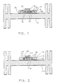
- the interface device 10 is coupled to an integrated circuit 12 and an underlying heat sink 14.
- the interface device 10 primarily comprises a first material 16 which is characterized by high thermal conductivity or low thermal resistance.
- a second material 18 which is characterized by a low coefficient of thermal expansion is dispersed as a plurality of regions throughout the first material 16. This first material 16 completely surrounds each region of second material 18.
- the preferred first material 16 which is characterized by a high thermal conductivity is copper, however other materials characterized by high thermal conductivity, such as aluminium, may also be used.
- a consideration when choosing the first material 16 is that the first material 16 must be compatible with the second material 18 which will be dispersed throughout the first material 16.
- copper is preferred because of its high thermal conductivity, cost and ease of manufacturability.
- the plurality of second material 18 regions comprise a material characterized by a low coefficient of thermal expansion, such as an iron-nickel alloy.
- a material characterized by a low coefficient of thermal expansion such as an iron-nickel alloy.
- an iron-nickel alloy comprising approximately 42 percent nickel and and approximately 58 percent iron such as Invar is preferred.
- other materials which are characterized by a low coefficient of thermal expansion and which are compatible with the surrounding first material 16 may also be used.
- a silicon integrated circuit chip 12 is soldered, the solder being denoted as layer 20, to an upper surface 22 of the primarily copper interface device 10 and an aluminium or copper heat sink 14 is bolted to a lower surface 24 of the primarily copper interface device 10.
- the preferred solder is a 25/75 tin-lead type for manufacturability and availability purposes, however other suitable solders may also be used.
- silicon grease (denoted as layer 26) is placed between the lower surface 24 of the interface device 10 and the heat sink 14.
- the silicon grease 26 is preferred since it permits heat transfer through to the heat sink 14 from the interface device 10, however, other suitable materials which will provide the appropriate heat transfer through to the heat sink 14 from the interface device 10 may also be used, such as suitable epoxy resins or solder.
- the low-expansion second material regions 18 are primarily located under the silicon integrated circuit chip 12 in the surrounding copper or other appropriate first material 16. It is desirable to position the low-expansion second material regions 18 primarily under the silicon chip 12 because the silicon expands at a much lower rate, as its temperature is increased, than the other materials. Therefore, the expansion of the interface device 10 is retarded most where it is required, i.e., under the silicon chip 12, with this design.
- the number of low-expansion second material regions 18 may vary within the surrounding copper material 16. As shown in Figure 1, there are four low-expansion regions 18 primarily situated under the integrated circuit chip 12 within the surrounding copper material 16. The arrows indicate the pattern of heat flow from the integrated circuit chip 12 to the heat sink 14 through the interface device 10. With this device 10, heat transfer occurs most efficiently. The heat generated by the integrated circuit chip 12 flows directly into the interface device 10, dissipating through the highly conductive surrounding copper layer 16 wherein the heat transfers rapidly through the copper layer 16 into the heat sink 14.
- a truly inventive feature of this device 10 is that the low-expansion regions 18 retard the expansion rate of the device 10 where it is most needed under the silicon chip 12, but do not hamper the heat flow from the silicon chip 12 to the heat sink 14 since the highly conductive surrounding copper layer 16 is provided generally everywhere throughout the device 10.
- the low-expansion material which is typically characterized by high thermal resistivity, acted as a barrier against effective heat transfer out of the chip 12. The heat was forced to go around the low-expansion material/high-resistivity material, resulting in an inefficient method of heat transfer. With this design, the heat does not need to go around the low-expansion second material 18, as there are continuous paths of high conductivity copper straight from the integrated circuit chip 12 to the heat sink 14.
- this interface device 10 is characterized by enhanced and efficient thermal dissipation yet provides a compatible coefficient of thermal expansion with the silicon integrated circuit 12 and underlying heat sink 14.
- an alternative and equally preferred embodiment 110 of this invention is also illustrated.
- this interface device 110 there are essentially two rows of low-expansion second material 118 enveloped by surrounding copper or other high-conductivity material 116.
- This device 110 permits enhanced heat transfer through the surrounding copper 116 and is characterized by an appropriate expansion rate.
- a device 110 in accordance with this invention could have as few as two low-expansion regions 118 separated by the copper 116 under a silicon chip 112 thereby providing a single direct path for heat transfer from the silicon chip 112 to a heat sink 114, or a multitude of low-expansion regions wherein the only limitations would be manufacturing and feasibility considerations.
- This interface device 110 may also be used when dielectric isolation is required, such as between a power-producing integrated circuit 212 and a heat sink 214.
- the dielectric isolation is provided by a polyimide layer 228, which has a thermally-conductive material dispersed throughout for enhanced thermal conductivity characteristics.
- the polyimide layer 228 is attached to the heat sink 214 by a very thin layer of thermally-conductive adhesive 230.
- the dielectric means, or polyimide layer 228, is preferably formed from a plastics dielectric material, such as Kapton. It is even more preferred that this dielectric layer 228 have dispersed throughout a suitable dielectric material having relatively high thermal conductivity, such as alumina, aluminum nitride or beryllium oxide.
- the thermally-conductive adhesive layer 230 used to attach the dielectric layer 228 to the heat sink 214 is preferably formed from an epoxy resin paste having silver or other appropriate thermally-conductive medium dispersed throughout.
- This medium may also be electrically conductive since the dielectric isolation is provided by layer 228.
- the silver-filled epoxy resin layer 230 is used for its convenience and availability, however other materials such as commercially-available B-staged epoxy resins, which are partially cured pastes, may also be used.
- a layer 226 of solder or other attachment means is required between the interface device 210 and dielectric layer 228. It is preferred that this solder layer 226 be formed from a 60/40 tin-lead solder. This is preferred because the solder layer 220 used to attach the integrated circuit 212 to the interface device 210 is a 25/75 lead-tin solder and this combination of solders having differing melting temperatures permits ease of manufacturability without detrimental effects to the complete structure.
- a flash metallization layer (not shown) may be required on the dielectric layer 228 to promote adhesion between the dielectric layer 228 and the solder layer 226, as well as between the dielectric layer 228 and the thermally-conductive adhesive layer 230.
- the structure shown in Figure 3 provides dielectric isolation when necessary between an integrated circuit chip 212 and heat sink 214.
- the coefficient of thermal expansion of the preferred interface device should be no more than about 10X10 ⁇ 6/°C. This is the maximum expansion rate that is desirable.
- the coefficient of thermal expansion for the silicon integrated circuit chip is approximately equal to about 3.5X10 ⁇ 6/°C, whilst the coefficient of thermal expansion for an aluminium heat sink is approximately 24X10 ⁇ 6/°C.
- the coefficients of thermal expansion for copper and an iron-nickel alloy containing approximately 42 percent nickel are 17.7X10 ⁇ 6/°C and about 2.7X10 ⁇ 6/°C, respectively.
- CTE coefficient of thermal expansion
- a first method comprises the steps of sandwiching a perforate layer of low-expansion material between two outer layers of copper and appropriately heating the materials so as to metallurgically bond the materials together.
- the perforate layer of low-expansion material may be formed by punching, piercing, dissolution or any other suitable means.
- a perforate layer 50 as shown in Figure 4, overlaying a single layer 52 of copper or other appropriate high thermal conductivity material, is preferably provided only in a centre region of the sandwiched layers (only the bottom layer 52 is shown in Figure 4 for clarity), so as to correspond to the region where the integrated circuit chip will be disposed.
- FIG. 5 shows the interface device 10 illustrated in Figure 1 which comprises a plurality of low-expansion second material regions 18 which were formed from the perforate layer (50 in Figure 4), surrounded by the high thermal conductivity material 16 which flowed into the perforations during heat treatment.
- the device having a cross-section as shown in Figures 2 or 3 may be formed by sandwiching a plurality of perforate layers between alternating layers of copper. Theoretically, the device could have a multitude of these layers, the only limit being manufacturability and feasibility. However, a device having two perforate layers sandwiched between three alternating layers of copper is preferred.
- the device could be fabricated by sandwiching strips of low-expansion wire between alternating layers of copper, and subsequently heat treating the sandwich thus formed to metallurgically bond the materials together. Again this would produce the desired result wherein the high conductivity copper completely surrounds a plurality of regions containing the low-expansion material.
- this alternative embodiment performs satisfactorily, it is not as preferred as the perforated embodiment which provides better control of the coefficient of thermal expansion properties of the device in both lateral directions, i.e., the x and y-axis of the device.
- This invention readily provides an interface device which promotes efficient heat transfer between a heat-generating integrated circuit chip and a heat sink, whilst also providing an intermediate and compatible coefficient of thermal expansion between the two components.
Landscapes
- Cooling Or The Like Of Semiconductors Or Solid State Devices (AREA)
- Cooling Or The Like Of Electrical Apparatus (AREA)
Applications Claiming Priority (4)
| Application Number | Priority Date | Filing Date | Title |
|---|---|---|---|
| US31838989A | 1989-03-03 | 1989-03-03 | |
| US318389 | 1989-03-03 | ||
| US07/422,395 US5151777A (en) | 1989-03-03 | 1989-10-16 | Interface device for thermally coupling an integrated circuit to a heat sink |
| US422395 | 1989-10-16 |
Publications (2)
| Publication Number | Publication Date |
|---|---|
| EP0385605A2 true EP0385605A2 (fr) | 1990-09-05 |
| EP0385605A3 EP0385605A3 (fr) | 1991-03-27 |
Family
ID=26981455
Family Applications (1)
| Application Number | Title | Priority Date | Filing Date |
|---|---|---|---|
| EP19900301513 Withdrawn EP0385605A3 (fr) | 1989-03-03 | 1990-02-13 | Dispositif intercalaire entre circuit intégré et dissipateur thermique |
Country Status (3)
| Country | Link |
|---|---|
| US (1) | US5151777A (fr) |
| EP (1) | EP0385605A3 (fr) |
| JP (1) | JPH02283053A (fr) |
Cited By (12)
| Publication number | Priority date | Publication date | Assignee | Title |
|---|---|---|---|---|
| US5156923A (en) * | 1992-01-06 | 1992-10-20 | Texas Instruments Incorporated | Heat-transferring circuit substrate with limited thermal expansion and method for making |
| WO1996037915A1 (fr) * | 1995-05-26 | 1996-11-28 | Sheldahl, Inc. | Film adhesif a faible impedance thermique et haute impedance electrique utilise dans un ensemble electronique a puits thermique |
| GB2311414A (en) * | 1996-03-21 | 1997-09-24 | Furukawa Electric Co Ltd | Composite substrate for a heat-generating semiconductor device |
| US6045927A (en) * | 1996-05-22 | 2000-04-04 | Hitachi Metals, Ltd. | Composite material for electronic part and method of producing same |
| US6129993A (en) * | 1998-02-13 | 2000-10-10 | Hitachi Metals, Ltd. | Heat spreader and method of making the same |
| FR2842942A1 (fr) * | 2002-07-26 | 2004-01-30 | Toyota Jidoshokki Kk | Systeme de radiateur, procede de rayonnement, tampon thermique, module a semi-conducteur, repartiteur de chaleur et substrat |
| EP1406298A1 (fr) * | 2002-10-03 | 2004-04-07 | Kabushiki Kaisha Toyota Jidoshokki | Module semi-conducteur et connecteur plat |
| FR2849804A1 (fr) * | 2003-01-15 | 2004-07-16 | Toyota Jidoshokki Kk | Materiau composite et procede pour le produire |
| EP1761114A2 (fr) * | 2005-08-31 | 2007-03-07 | Kabushiki Kaisha Toyota Jidoshokki | Plaquette à circuits |
| EP1538667A3 (fr) * | 2003-12-06 | 2007-04-18 | LuK Lamellen und Kupplungsbau Beteiligungs KG | Appareil électronique avec un corps dissipateur de chaleur metallique eléctriquement isolé |
| EP1422756A4 (fr) * | 2001-08-28 | 2008-04-09 | Toyota Jidoshokki Kk | Materiau structural composite et procede de production dudit materiau |
| WO2010057236A3 (fr) * | 2008-11-20 | 2011-05-12 | Plansee Se | Puits thermique et procédé de fabrication |
Families Citing this family (40)
| Publication number | Priority date | Publication date | Assignee | Title |
|---|---|---|---|---|
| JPH04291948A (ja) * | 1991-03-20 | 1992-10-16 | Fujitsu Ltd | 半導体装置及びその製造方法及び放熱フィン |
| US5213868A (en) * | 1991-08-13 | 1993-05-25 | Chomerics, Inc. | Thermally conductive interface materials and methods of using the same |
| US5310520A (en) * | 1993-01-29 | 1994-05-10 | Texas Instruments Incorporated | Circuit system, a composite material for use therein, and a method of making the material |
| US5886407A (en) * | 1993-04-14 | 1999-03-23 | Frank J. Polese | Heat-dissipating package for microcircuit devices |
| US5972737A (en) * | 1993-04-14 | 1999-10-26 | Frank J. Polese | Heat-dissipating package for microcircuit devices and process for manufacture |
| US6432497B2 (en) | 1997-07-28 | 2002-08-13 | Parker-Hannifin Corporation | Double-side thermally conductive adhesive tape for plastic-packaged electronic components |
| US6400012B1 (en) * | 1997-09-17 | 2002-06-04 | Advanced Energy Voorhees, Inc. | Heat sink for use in cooling an integrated circuit |
| US6096414A (en) * | 1997-11-25 | 2000-08-01 | Parker-Hannifin Corporation | High dielectric strength thermal interface material |
| US6207294B1 (en) * | 1999-04-30 | 2001-03-27 | Philip A. Rutter | Self-sharpening, laminated cutting tool and method for making the tool |
| JP2002118202A (ja) * | 2000-10-05 | 2002-04-19 | Sanyo Electric Co Ltd | 放熱基板および半導体モジュール |
| US6965071B2 (en) * | 2001-05-10 | 2005-11-15 | Parker-Hannifin Corporation | Thermal-sprayed metallic conformal coatings used as heat spreaders |
| US7006354B2 (en) * | 2001-10-26 | 2006-02-28 | Fujikura Ltd. | Heat radiating structure for electronic device |
| US6802446B2 (en) * | 2002-02-01 | 2004-10-12 | Delphi Technologies, Inc. | Conductive adhesive material with metallurgically-bonded conductive particles |
| JP3788410B2 (ja) * | 2002-08-27 | 2006-06-21 | 株式会社豊田自動織機 | 低膨張板の製造方法 |
| JP3933014B2 (ja) * | 2002-08-27 | 2007-06-20 | 松下電工株式会社 | 植物育成貯蔵装置 |
| US8119191B2 (en) * | 2003-01-16 | 2012-02-21 | Parker-Hannifin Corporation | Dispensable cured resin |
| US7268425B2 (en) * | 2003-03-05 | 2007-09-11 | Intel Corporation | Thermally enhanced electronic flip-chip packaging with external-connector-side die and method |
| US6873043B2 (en) * | 2003-03-10 | 2005-03-29 | Delphi Technologies, Inc. | Electronic assembly having electrically-isolated heat-conductive structure |
| US7147041B2 (en) * | 2004-05-03 | 2006-12-12 | Parker-Hannifin Corporation | Lightweight heat sink |
| JP4354377B2 (ja) * | 2004-09-28 | 2009-10-28 | 三菱電機株式会社 | 半導体装置 |
| US7954236B2 (en) | 2007-02-08 | 2011-06-07 | Lundell Manufacturing Corporation | Method of assembling a sealed thermal interface |
| US8448693B2 (en) * | 2007-02-08 | 2013-05-28 | Lundell Manufacturing Corporation | Sealed thermal interface component |
| US7834447B2 (en) * | 2007-05-22 | 2010-11-16 | Centipede Systems, Inc. | Compliant thermal contactor |
| US7719816B2 (en) | 2007-05-22 | 2010-05-18 | Centipede Systems, Inc. | Compliant thermal contactor |
| US20090141456A1 (en) * | 2007-11-30 | 2009-06-04 | Itt Manufacturing Enterprises, Inc. | Multilayer, thermally-stabilized substrate structures |
| WO2011019719A1 (fr) | 2009-08-12 | 2011-02-17 | Parker-Hannifin Corporation | Agent de remplissage d'espace formé en place totalement durci thermiquement ou électriquement conducteur |
| JP5837754B2 (ja) * | 2011-03-23 | 2015-12-24 | Dowaメタルテック株式会社 | 金属−セラミックス接合基板およびその製造方法 |
| US8778259B2 (en) | 2011-05-25 | 2014-07-15 | Gerhard B. Beckmann | Self-renewing cutting surface, tool and method for making same using powder metallurgy and densification techniques |
| JP6154987B2 (ja) * | 2011-09-22 | 2017-06-28 | 新電元工業株式会社 | 半導体装置 |
| JP6179003B2 (ja) * | 2011-09-22 | 2017-08-16 | 新電元工業株式会社 | 半導体装置 |
| US8743545B2 (en) | 2011-10-12 | 2014-06-03 | International Business Machines Corporation | Thermal expansion-enhanced heat sink for an electronic assembly |
| US9207002B2 (en) | 2011-10-12 | 2015-12-08 | International Business Machines Corporation | Contaminant separator for a vapor-compression refrigeration apparatus |
| JP2013098451A (ja) * | 2011-11-04 | 2013-05-20 | Sumitomo Electric Ind Ltd | 半導体装置及び配線基板 |
| JP6224960B2 (ja) * | 2012-09-27 | 2017-11-01 | Dowaメタルテック株式会社 | 放熱板およびその製造方法 |
| EP3058591B1 (fr) * | 2013-10-18 | 2020-11-18 | Griset | Support pour composants électroniques de puissance, module de puissance doté d'un tel support, et procédé de fabrication correspondant |
| US9524917B2 (en) | 2014-04-23 | 2016-12-20 | Optiz, Inc. | Chip level heat dissipation using silicon |
| CN106449567B (zh) * | 2016-11-26 | 2018-11-23 | 江苏拓博制冷科技有限公司 | 一种冷却器 |
| JP6867243B2 (ja) * | 2017-06-26 | 2021-04-28 | 新光電気工業株式会社 | 放熱板及びその製造方法と電子部品装置 |
| CN109219320B (zh) * | 2018-10-31 | 2020-12-29 | 北京地平线机器人技术研发有限公司 | 电子设备及其散热装置和车辆设备 |
| EP4301805A1 (fr) | 2021-03-04 | 2024-01-10 | Momentive Performance Materials Inc. | Composition de gel thermique |
Family Cites Families (18)
| Publication number | Priority date | Publication date | Assignee | Title |
|---|---|---|---|---|
| US3399332A (en) * | 1965-12-29 | 1968-08-27 | Texas Instruments Inc | Heat-dissipating support for semiconductor device |
| US3846824A (en) * | 1973-06-13 | 1974-11-05 | Gen Electric | Improved thermally conductive and electrically insulative mounting systems for heat sinks |
| JPS5116302B2 (fr) * | 1973-10-22 | 1976-05-22 | ||
| JPS603776B2 (ja) * | 1977-06-03 | 1985-01-30 | 株式会社日立製作所 | 半導体素子 |
| US4320412A (en) * | 1977-06-23 | 1982-03-16 | Western Electric Co., Inc. | Composite material for mounting electronic devices |
| JPS5536915A (en) * | 1978-09-04 | 1980-03-14 | Hitachi Ltd | Electronic circuit and its manufacturing |
| JPS55128852A (en) * | 1979-03-27 | 1980-10-06 | Nec Corp | Insulating type semiconductor device |
| US4283464A (en) * | 1979-05-08 | 1981-08-11 | Norman Hascoe | Prefabricated composite metallic heat-transmitting plate unit |
| EP0042693B1 (fr) * | 1980-06-21 | 1985-03-27 | LUCAS INDUSTRIES public limited company | Composant de puissance à semi-conducteur et procédé pour sa fabrication |
| US4427993A (en) * | 1980-11-21 | 1984-01-24 | General Electric Company | Thermal stress relieving bimetallic plate |
| JPS57130441A (en) * | 1981-02-06 | 1982-08-12 | Hitachi Ltd | Integrated circuit device |
| JPS5861677A (ja) * | 1981-10-09 | 1983-04-12 | Toshiba Corp | 半導体装置 |
| US4401798A (en) * | 1982-04-22 | 1983-08-30 | Tenneco Polymers, Inc. | Process for the production of vinyl halide polymers that uses an alkyl-substituted trisphenol as the chain-terminating agent |
| US4554575A (en) * | 1983-05-12 | 1985-11-19 | Westinghouse Electric Corp. | Low stress leadless chip carrier and method of assembly |
| JPS6015241A (ja) * | 1983-07-07 | 1985-01-25 | Iseki & Co Ltd | キヤビン後部窓のウオツシヤ |
| JPS6027151A (ja) * | 1983-07-25 | 1985-02-12 | Sumitomo Electric Ind Ltd | 半導体素子搭載用複合金属条 |
| JPS61156754A (ja) * | 1984-12-27 | 1986-07-16 | Matsushita Electric Ind Co Ltd | 高熱伝導性金属ベ−スプリント基板 |
| US4811166A (en) * | 1986-07-02 | 1989-03-07 | Texas Instruments Incorporated | Heat dissipating member for mounting a semiconductor device and electrical circuit unit incorporating the member |
-
1989
- 1989-10-16 US US07/422,395 patent/US5151777A/en not_active Expired - Lifetime
-
1990
- 1990-02-13 EP EP19900301513 patent/EP0385605A3/fr not_active Withdrawn
- 1990-03-01 JP JP2050811A patent/JPH02283053A/ja active Pending
Non-Patent Citations (2)
| Title |
|---|
| PATENT ABSTRACTS OF JAPAN, unexamined applications, E field, vol. 4, no. 185, December 19, 1980 THE PATENT OFFICE JAPANESE GOVERNMENT page 65 E 38 * JP - A - 55 - 127 044 ( HITACHI SEISAKUSHO K.K. ) * * |
| PATENT ABSTRACTS OF JAPAN, unexamined applications, E field, vol. 5, no. 34, March 4, 1981 THE PATENT OFFICE JAPANESE GOVERNMENT page 160 E 48 * JP - A - 55 - 162 249 ( HITACHI SEISAKUSHO K.K. ) * * |
Cited By (15)
| Publication number | Priority date | Publication date | Assignee | Title |
|---|---|---|---|---|
| US5156923A (en) * | 1992-01-06 | 1992-10-20 | Texas Instruments Incorporated | Heat-transferring circuit substrate with limited thermal expansion and method for making |
| EP0550999A1 (fr) * | 1992-01-06 | 1993-07-14 | Texas Instruments Incorporated | Substrat de circuit transférant la chaleur possédant une dilatation thermique limitée et son procédé de production |
| WO1996037915A1 (fr) * | 1995-05-26 | 1996-11-28 | Sheldahl, Inc. | Film adhesif a faible impedance thermique et haute impedance electrique utilise dans un ensemble electronique a puits thermique |
| GB2311414A (en) * | 1996-03-21 | 1997-09-24 | Furukawa Electric Co Ltd | Composite substrate for a heat-generating semiconductor device |
| GB2311414B (en) * | 1996-03-21 | 1999-07-07 | Furukawa Electric Co Ltd | Composite substrate for heat-generating semiconductor device and semiconductor apparatus using the same |
| US6045927A (en) * | 1996-05-22 | 2000-04-04 | Hitachi Metals, Ltd. | Composite material for electronic part and method of producing same |
| US6129993A (en) * | 1998-02-13 | 2000-10-10 | Hitachi Metals, Ltd. | Heat spreader and method of making the same |
| EP1422756A4 (fr) * | 2001-08-28 | 2008-04-09 | Toyota Jidoshokki Kk | Materiau structural composite et procede de production dudit materiau |
| FR2842942A1 (fr) * | 2002-07-26 | 2004-01-30 | Toyota Jidoshokki Kk | Systeme de radiateur, procede de rayonnement, tampon thermique, module a semi-conducteur, repartiteur de chaleur et substrat |
| EP1406298A1 (fr) * | 2002-10-03 | 2004-04-07 | Kabushiki Kaisha Toyota Jidoshokki | Module semi-conducteur et connecteur plat |
| FR2849804A1 (fr) * | 2003-01-15 | 2004-07-16 | Toyota Jidoshokki Kk | Materiau composite et procede pour le produire |
| US6994917B2 (en) | 2003-01-15 | 2006-02-07 | Kabushiki Kaisha Toyota Jidoshokki | Composite material and method for manufacturing the same |
| EP1538667A3 (fr) * | 2003-12-06 | 2007-04-18 | LuK Lamellen und Kupplungsbau Beteiligungs KG | Appareil électronique avec un corps dissipateur de chaleur metallique eléctriquement isolé |
| EP1761114A2 (fr) * | 2005-08-31 | 2007-03-07 | Kabushiki Kaisha Toyota Jidoshokki | Plaquette à circuits |
| WO2010057236A3 (fr) * | 2008-11-20 | 2011-05-12 | Plansee Se | Puits thermique et procédé de fabrication |
Also Published As
| Publication number | Publication date |
|---|---|
| EP0385605A3 (fr) | 1991-03-27 |
| JPH02283053A (ja) | 1990-11-20 |
| US5151777A (en) | 1992-09-29 |
Similar Documents
| Publication | Publication Date | Title |
|---|---|---|
| EP0385605A2 (fr) | Dispositif intercalaire entre circuit intégré et dissipateur thermique | |
| JP3084230B2 (ja) | ボール・グリッド・アレイ・パッケージ | |
| JP2548350B2 (ja) | テープ自動結合に使用される熱放散相互接続テープ | |
| US5650662A (en) | Direct bonded heat spreader | |
| EP0120500B1 (fr) | Empaquetage pour LSI à haute densité pour circuits logiques | |
| US5455457A (en) | Package for semiconductor elements having thermal dissipation means | |
| JP2988243B2 (ja) | パワー混成集積回路装置 | |
| EP0553463B1 (fr) | Emballage électronique avec déviation élevée de la chaleur et procédé pour faire celui-ci | |
| JPH0231499B2 (fr) | ||
| EP1345265B1 (fr) | Ensemble électronique avec un dissipateur de chaleur de configuration améliorée | |
| EP0696882B1 (fr) | Plaque à circuits imprimés avec un dissipateur de chaleur bimétallique | |
| US7151308B2 (en) | Semiconductor chip package | |
| US6351389B1 (en) | Device and method for packaging an electronic device | |
| EP1610381B1 (fr) | Boîtier électronique avec connexions segmentées et joint soudé | |
| JPH01235261A (ja) | 半導体装置及びその製造方法 | |
| EP1336993B1 (fr) | Structure d'assemblage pour circuit intégré de puissance formée sur une puce semiconductrice et procédé de fabrication | |
| JP3972519B2 (ja) | パワー半導体モジュール | |
| JP2865496B2 (ja) | マルチチップモジュール | |
| EP0525651B1 (fr) | Structure d'empaquetage pour un ou plusieurs circuits intégrés | |
| EP0523387A2 (fr) | Module à puce semi-conducteur et procédé pour sa fabrication | |
| JPS6220701B2 (fr) | ||
| EP0661739A2 (fr) | Boîtier à réseau de broches | |
| JPS62281453A (ja) | チツプキヤリアモジユ−ル | |
| JPS5835956A (ja) | 混成集積回路装置 | |
| JPS6220702B2 (fr) |
Legal Events
| Date | Code | Title | Description |
|---|---|---|---|
| PUAI | Public reference made under article 153(3) epc to a published international application that has entered the european phase |
Free format text: ORIGINAL CODE: 0009012 |
|
| AK | Designated contracting states |
Kind code of ref document: A2 Designated state(s): DE FR IT |
|
| PUAL | Search report despatched |
Free format text: ORIGINAL CODE: 0009013 |
|
| AK | Designated contracting states |
Kind code of ref document: A3 Designated state(s): DE FR IT |
|
| 17P | Request for examination filed |
Effective date: 19910507 |
|
| 17Q | First examination report despatched |
Effective date: 19930614 |
|
| STAA | Information on the status of an ep patent application or granted ep patent |
Free format text: STATUS: THE APPLICATION IS DEEMED TO BE WITHDRAWN |
|
| 18D | Application deemed to be withdrawn |
Effective date: 19931026 |