EP0386676A2 - Procédé de croissance de semi-conducteur et appareillage pour cela - Google Patents
Procédé de croissance de semi-conducteur et appareillage pour cela Download PDFInfo
- Publication number
- EP0386676A2 EP0386676A2 EP90104205A EP90104205A EP0386676A2 EP 0386676 A2 EP0386676 A2 EP 0386676A2 EP 90104205 A EP90104205 A EP 90104205A EP 90104205 A EP90104205 A EP 90104205A EP 0386676 A2 EP0386676 A2 EP 0386676A2
- Authority
- EP
- European Patent Office
- Prior art keywords
- growth
- substrate
- semiconductor layer
- reaction vessel
- heating
- Prior art date
- Legal status (The legal status is an assumption and is not a legal conclusion. Google has not performed a legal analysis and makes no representation as to the accuracy of the status listed.)
- Ceased
Links
Images


Classifications
-
- H—ELECTRICITY
- H10—SEMICONDUCTOR DEVICES; ELECTRIC SOLID-STATE DEVICES NOT OTHERWISE PROVIDED FOR
- H10P—GENERIC PROCESSES OR APPARATUS FOR THE MANUFACTURE OR TREATMENT OF DEVICES COVERED BY CLASS H10
- H10P14/00—Formation of materials, e.g. in the shape of layers or pillars
- H10P14/20—Formation of materials, e.g. in the shape of layers or pillars of semiconductor materials
- H10P14/29—Formation of materials, e.g. in the shape of layers or pillars of semiconductor materials characterised by the substrates
- H10P14/2901—Materials
- H10P14/2902—Materials being Group IVA materials
- H10P14/2905—Silicon, silicon germanium or germanium
-
- B—PERFORMING OPERATIONS; TRANSPORTING
- B82—NANOTECHNOLOGY
- B82Y—SPECIFIC USES OR APPLICATIONS OF NANOSTRUCTURES; MEASUREMENT OR ANALYSIS OF NANOSTRUCTURES; MANUFACTURE OR TREATMENT OF NANOSTRUCTURES
- B82Y10/00—Nanotechnology for information processing, storage or transmission, e.g. quantum computing or single electron logic
-
- H—ELECTRICITY
- H10—SEMICONDUCTOR DEVICES; ELECTRIC SOLID-STATE DEVICES NOT OTHERWISE PROVIDED FOR
- H10D—INORGANIC ELECTRIC SEMICONDUCTOR DEVICES
- H10D10/00—Bipolar junction transistors [BJT]
- H10D10/01—Manufacture or treatment
- H10D10/051—Manufacture or treatment of vertical BJTs
- H10D10/054—Forming extrinsic base regions on silicon substrate after insulating device isolation in vertical BJTs having single crystalline emitter, collector or base regions
-
- H—ELECTRICITY
- H10—SEMICONDUCTOR DEVICES; ELECTRIC SOLID-STATE DEVICES NOT OTHERWISE PROVIDED FOR
- H10D—INORGANIC ELECTRIC SEMICONDUCTOR DEVICES
- H10D62/00—Semiconductor bodies, or regions thereof, of devices having potential barriers
- H10D62/80—Semiconductor bodies, or regions thereof, of devices having potential barriers characterised by the materials
- H10D62/82—Heterojunctions
- H10D62/822—Heterojunctions comprising only Group IV materials heterojunctions, e.g. Si/Ge heterojunctions
-
- H—ELECTRICITY
- H10—SEMICONDUCTOR DEVICES; ELECTRIC SOLID-STATE DEVICES NOT OTHERWISE PROVIDED FOR
- H10P—GENERIC PROCESSES OR APPARATUS FOR THE MANUFACTURE OR TREATMENT OF DEVICES COVERED BY CLASS H10
- H10P14/00—Formation of materials, e.g. in the shape of layers or pillars
- H10P14/20—Formation of materials, e.g. in the shape of layers or pillars of semiconductor materials
- H10P14/24—Formation of materials, e.g. in the shape of layers or pillars of semiconductor materials using chemical vapour deposition [CVD]
-
- H—ELECTRICITY
- H10—SEMICONDUCTOR DEVICES; ELECTRIC SOLID-STATE DEVICES NOT OTHERWISE PROVIDED FOR
- H10P—GENERIC PROCESSES OR APPARATUS FOR THE MANUFACTURE OR TREATMENT OF DEVICES COVERED BY CLASS H10
- H10P14/00—Formation of materials, e.g. in the shape of layers or pillars
- H10P14/20—Formation of materials, e.g. in the shape of layers or pillars of semiconductor materials
- H10P14/32—Formation of materials, e.g. in the shape of layers or pillars of semiconductor materials characterised by intermediate layers between substrates and deposited layers
- H10P14/3202—Materials thereof
- H10P14/3204—Materials thereof being Group IVA semiconducting materials
- H10P14/3211—Silicon, silicon germanium or germanium
-
- H—ELECTRICITY
- H10—SEMICONDUCTOR DEVICES; ELECTRIC SOLID-STATE DEVICES NOT OTHERWISE PROVIDED FOR
- H10P—GENERIC PROCESSES OR APPARATUS FOR THE MANUFACTURE OR TREATMENT OF DEVICES COVERED BY CLASS H10
- H10P14/00—Formation of materials, e.g. in the shape of layers or pillars
- H10P14/20—Formation of materials, e.g. in the shape of layers or pillars of semiconductor materials
- H10P14/34—Deposited materials, e.g. layers
- H10P14/3402—Deposited materials, e.g. layers characterised by the chemical composition
- H10P14/3404—Deposited materials, e.g. layers characterised by the chemical composition being Group IVA materials
- H10P14/3411—Silicon, silicon germanium or germanium
-
- H—ELECTRICITY
- H10—SEMICONDUCTOR DEVICES; ELECTRIC SOLID-STATE DEVICES NOT OTHERWISE PROVIDED FOR
- H10P—GENERIC PROCESSES OR APPARATUS FOR THE MANUFACTURE OR TREATMENT OF DEVICES COVERED BY CLASS H10
- H10P14/00—Formation of materials, e.g. in the shape of layers or pillars
- H10P14/20—Formation of materials, e.g. in the shape of layers or pillars of semiconductor materials
- H10P14/34—Deposited materials, e.g. layers
- H10P14/3438—Doping during depositing
- H10P14/3441—Conductivity type
- H10P14/3442—N-type
-
- H—ELECTRICITY
- H10—SEMICONDUCTOR DEVICES; ELECTRIC SOLID-STATE DEVICES NOT OTHERWISE PROVIDED FOR
- H10P—GENERIC PROCESSES OR APPARATUS FOR THE MANUFACTURE OR TREATMENT OF DEVICES COVERED BY CLASS H10
- H10P14/00—Formation of materials, e.g. in the shape of layers or pillars
- H10P14/20—Formation of materials, e.g. in the shape of layers or pillars of semiconductor materials
- H10P14/34—Deposited materials, e.g. layers
- H10P14/3438—Doping during depositing
- H10P14/3441—Conductivity type
- H10P14/3444—P-type
-
- H—ELECTRICITY
- H10—SEMICONDUCTOR DEVICES; ELECTRIC SOLID-STATE DEVICES NOT OTHERWISE PROVIDED FOR
- H10D—INORGANIC ELECTRIC SEMICONDUCTOR DEVICES
- H10D30/00—Field-effect transistors [FET]
- H10D30/01—Manufacture or treatment
- H10D30/014—Manufacture or treatment of FETs having zero-dimensional [0D] or one-dimensional [1D] channels, e.g. quantum wire FETs, single-electron transistors [SET] or Coulomb blockade transistors
-
- H—ELECTRICITY
- H10—SEMICONDUCTOR DEVICES; ELECTRIC SOLID-STATE DEVICES NOT OTHERWISE PROVIDED FOR
- H10D—INORGANIC ELECTRIC SEMICONDUCTOR DEVICES
- H10D30/00—Field-effect transistors [FET]
- H10D30/40—FETs having zero-dimensional [0D], one-dimensional [1D] or two-dimensional [2D] charge carrier gas channels
- H10D30/43—FETs having zero-dimensional [0D], one-dimensional [1D] or two-dimensional [2D] charge carrier gas channels having one-dimensional [1D] charge carrier gas channels, e.g. quantum wire FETs or transistors having 1D quantum-confined channels
-
- Y—GENERAL TAGGING OF NEW TECHNOLOGICAL DEVELOPMENTS; GENERAL TAGGING OF CROSS-SECTIONAL TECHNOLOGIES SPANNING OVER SEVERAL SECTIONS OF THE IPC; TECHNICAL SUBJECTS COVERED BY FORMER USPC CROSS-REFERENCE ART COLLECTIONS [XRACs] AND DIGESTS
- Y10—TECHNICAL SUBJECTS COVERED BY FORMER USPC
- Y10S—TECHNICAL SUBJECTS COVERED BY FORMER USPC CROSS-REFERENCE ART COLLECTIONS [XRACs] AND DIGESTS
- Y10S148/00—Metal treatment
- Y10S148/025—Deposition multi-step
-
- Y—GENERAL TAGGING OF NEW TECHNOLOGICAL DEVELOPMENTS; GENERAL TAGGING OF CROSS-SECTIONAL TECHNOLOGIES SPANNING OVER SEVERAL SECTIONS OF THE IPC; TECHNICAL SUBJECTS COVERED BY FORMER USPC CROSS-REFERENCE ART COLLECTIONS [XRACs] AND DIGESTS
- Y10—TECHNICAL SUBJECTS COVERED BY FORMER USPC
- Y10S—TECHNICAL SUBJECTS COVERED BY FORMER USPC CROSS-REFERENCE ART COLLECTIONS [XRACs] AND DIGESTS
- Y10S148/00—Metal treatment
- Y10S148/057—Gas flow control
-
- Y—GENERAL TAGGING OF NEW TECHNOLOGICAL DEVELOPMENTS; GENERAL TAGGING OF CROSS-SECTIONAL TECHNOLOGIES SPANNING OVER SEVERAL SECTIONS OF THE IPC; TECHNICAL SUBJECTS COVERED BY FORMER USPC CROSS-REFERENCE ART COLLECTIONS [XRACs] AND DIGESTS
- Y10—TECHNICAL SUBJECTS COVERED BY FORMER USPC
- Y10S—TECHNICAL SUBJECTS COVERED BY FORMER USPC CROSS-REFERENCE ART COLLECTIONS [XRACs] AND DIGESTS
- Y10S148/00—Metal treatment
- Y10S148/059—Germanium on silicon or Ge-Si on III-V
-
- Y—GENERAL TAGGING OF NEW TECHNOLOGICAL DEVELOPMENTS; GENERAL TAGGING OF CROSS-SECTIONAL TECHNOLOGIES SPANNING OVER SEVERAL SECTIONS OF THE IPC; TECHNICAL SUBJECTS COVERED BY FORMER USPC CROSS-REFERENCE ART COLLECTIONS [XRACs] AND DIGESTS
- Y10—TECHNICAL SUBJECTS COVERED BY FORMER USPC
- Y10S—TECHNICAL SUBJECTS COVERED BY FORMER USPC CROSS-REFERENCE ART COLLECTIONS [XRACs] AND DIGESTS
- Y10S148/00—Metal treatment
- Y10S148/16—Superlattice
Definitions
- the present invention relates to process and an apparatus for a semiconductor growth and more particularly, to a CVD process for producing a semiconductor epitaxial layer, and a CVD apparatus therefor.
- a thin epitaxial layer of a semiconductor material such as a silicon (Si), silicon germanium (SiGe) silicon carbide (SiC), etc.
- a CVD (Chemical Vapor Deposition) process, a MBE (Molecular Beam Epitaxial) process, a photo epitaxial growth process etc. are used.
- an MBE process and a photo epitaxial growth process are well known.
- the MBE process however, has problems in that the process is not suitable for mass production because of the necessity for a high vacuum condition, the poor crystallizability of a formed epitaxial layer, an epitaxial growth cannot be realized at a side wall of a semiconductor substrate, a selective growth cannot be carried out, and impurities cannot be doped into a semiconductor substrate to a high concentration, e.g., more than 1018/cm3.
- the photo epitaxial growth process has problems in that a mass productivity thereby defective in that the window for introducing the UV light becomes fogged, and an epitaxial growth cannot be realized at a side wall of a semiconductor substrate.
- An object of the present invention is to provide a semiconductor growth process whereby multilayers having a different composition of at least each neighbouring layer are grown.
- Another other object of the present invention is to provide a semiconductor growth process wherein a satisfactorily shallow epitaxial pn junction can be produced.
- a further object of the present invention is to provide a semiconductor growth apparatus whereby the above-mentioned process is carried out.
- a semiconductor growth process wherein a plurality of layers each consisting of a different kind of semiconductor material are grown, comprising the steps of: heating a substrate to a first growth starting temperature at which a growth of a first semiconductor layer can be started, supplying a first material gas to the surface of said substrate to cause a growth of said first semiconductor layer, lowering the temperature of said substrate to below said first growth starting temperature, and at the same time, stopping the supply of said first material gas, to stop the growth of said first semiconductor layer, heating said substrate to a second growth starting temperature at which a growth of a second semiconductor layer can be started, and supplying a second material gas to the surface of said substrate to cause a growth of said second semiconductor layer.
- a semiconductor growth apparatus comprising: a reaction vessel, wherein different kinds of lapped layers are grown on a substrate by introducing different kinds of gases for growth into a reaction vessel a heating unit far heating said substrate provided in the reaction vessel, a gas change-over unit for changing a plurality of gases for growth and a control unit for controlling said heating unit and said change-over unit so that at the same time as the temperature of said substrate reaches the growth temperature said gases for growth are introduced into said reaction vessel and at the same time as said gases for growth are changed, the heating of the substrate is stopped.
- an infrared heater such as tungsten halogen lamp or arc lamp, etc. can be used. In such heater temperature is increased by a rate of 40°C/sec and is lowered by a rate of 100°C/sec.
- Figure 1 shows a schematic view of a CVD apparatus according to the present invention.
- a wafer 3 of a silicon series semiconductor material such as Si, SiGe, SiC, etc. supported by pins 2 is provided, and an infrared heater 4 such as an arc lamp or a tungsten halogen lamp is provided above the reaction vessel, to heat the wafer 3.
- the infrared heater 4 is connected to an electric source 5 which an electric power is supplied thereto.
- the electric source 5 is connected to a gas supply and a heating controller 7, and the controller 7 is connected to a high speed gas change-over unit 6 consisting of carrier gas (H2) mass flow controllers (MFC) 8 and 9, reacting gas MFC's 10 to 12, and three-way valves 13 to 15.
- H2 carrier gas
- MFC mass flow controllers
- the high speed gas change-over unit at least two different kinds of gas compositions are introduced into the reaction vessel 1 so that at least two different epitaxial layers are grown on the wafer.
- H2 gas is supplied to the reaction vessel 1 as a carrier gas, at a flow rate of 1 l/min, and the atmosphere in the reaction vessel 1 is heated to a temperature of 900°C under a pressure of 5 Torr, to clean the p ⁇ substrate, for five minutes.
- the atmosphere in the reaction vessel 1 is preferably cooled to a temperature of 500°C. In this case 550°C may be used.
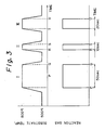
- the epitaxial growth sequence is shown in Figure 3, wherein the regions I, II and III corresponds to growth regions of an n ⁇ layer 19, a p-layer 20 and an n ⁇ layer 21 shown in Fig. 2, respectively, and the temperature of the atmosphere in the reaction vessel 1 is maintained at 500°C the controller increases the power supplied by the electronic source 5 just before a point P, to increase the temperature of the wafer 3 heated by the infrared heater 4.
- the controller 7 controls temperature of the wafer to 800°C at the point P (Fig. 3).
- SiH4 gas is introduced into the reaction vessel 1 at a flow rate of 100 cc/min.
- controller 7 When 50 sec. has passed (point Q) and the gas flow is stopped by the controller 7, the controller 7 simultaneously switches off the electric source 5 so that the temperature of the atmosphere in the reaction vessel 1 is lowered to a temperature of 500°C.
- the process causes a growth of an n ⁇ epitaxial layer 19 having a thickness of 5000 ⁇ on the substrate.
- the controller 7 again increases the power from the electric source 5 just before a point R (Fig. 3) to increase the temperature of the wafer 3 heated by the infrared heater 4.
- the controller 7 controls the temperature of the wafer to 800°C at the point R.
- This process sequence corresponds to the region II (R to 5).
- the H2 carrier gas flows together with the reaction gas at a flow rate of 1 l/min.
- SiH4 gas flows into the reaction vessel 1 at a flow rate of 100 cc/min.
- the controller 7 When the 10 sec has passed (point S) and the gas flow is stopped by the controller 7, the controller 7 simultaneously switches off the electric source 5 so that the temperature of the atmosphere in the reaction vessel 1 is lowered to a temperature of 500°C.
- This second process causes the growth of the p type epitaxial layer 21 having a thickness of 1000 ⁇ on the n ⁇ type epitaxial layer 19.
- the n ⁇ type epitaxial layer 21 having a thickness of 2000 ⁇ is grown on the p type epitaxial layer 20, using SiH4, AsH3 and H2 gases.
- the growth time from T to U is 20 sec.
- n ⁇ pn ⁇ type epitaxial layers 19, 20 and 21 have respective impurity concentrations of 5 X 10¹⁷, 3 x 10¹⁸ and 5 x 10²⁰, as shown in Figure 4.
- Figure 4 is an impurity profile obtained by a SIMS, and in Fig. 4 the regions I, II, and III correspond to the regions I, II, and III of Fig. 3.
- the region I corresponding to the n ⁇ type epitaxial layer 19 has a thickness of 5000 ⁇
- the region II corresponding to the p type epitaxial layer 20 has a thickness of 1000 ⁇
- the region III corresponding to the n ⁇ type epitaxial layer has a thickness of 2000 ⁇ .
- the right side of the region I is an n+ type well in the substrate.
- a very clear epitaxial pn junction can be formed.
- n ⁇ pn ⁇ type epitaxial layers 19, 20 and 21 mesa etching is carried out twice, and a passivation film of SiO2 is then formed on the n ⁇ type epitaxial layer 19, p type epitaxial layer 20, and the substrate 17, to a thickness of 2000 ⁇ , by a well known CVD process.
- a passivation film of SiO2 is then formed on the n ⁇ type epitaxial layer 19, p type epitaxial layer 20, and the substrate 17, to a thickness of 2000 ⁇ , by a well known CVD process.
- contact windows for the emitter base and collector are opened, and thereafter, Al-Si is sputtered to a thickness of 1 ⁇ m and selectively etched to form an emitter (E) electrode 23, a base (B) electrode 24, and a collector (C) electrode 25, whereby a bipolar transistor having the structure shown in Fig. 2 is produced.
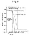
- Figure 5 is an example showing a sharpness of a pn boundary in the present invention.
- the present invention has a shorter impurity deviation distance (L1) in the depth direction than that (L2) of a prior art.
- Figure 6 shows a schematic cross-sectional view of a semiconductor element formed by using a quantum wire according to the present invention.
- a non-doped SiGe layer 31a, a non-doped Si layer 32a, a non-doped SiGe layer 31b, a non-doped Si layer 32b, a non-doped SiGe layer 31c, a non-doped Si layer 32c, and a non-doped SiGe layer 31d are formed on a silicon substrate 30.
- Quantum wire 40 are formed at the side of SiGe layers 31a, 31b, 31c and 31d.
- 33 is a p+ type epitaxial layer having a thickness of 500 ⁇ according to the present invention.
Landscapes
- Engineering & Computer Science (AREA)
- Chemical & Material Sciences (AREA)
- Nanotechnology (AREA)
- Physics & Mathematics (AREA)
- Mathematical Physics (AREA)
- Theoretical Computer Science (AREA)
- Crystallography & Structural Chemistry (AREA)
- Bipolar Transistors (AREA)
Applications Claiming Priority (2)
| Application Number | Priority Date | Filing Date | Title |
|---|---|---|---|
| JP1055827A JPH02235327A (ja) | 1989-03-08 | 1989-03-08 | 半導体成長装置および半導体成長方法 |
| JP55827/89 | 1989-03-08 |
Publications (2)
| Publication Number | Publication Date |
|---|---|
| EP0386676A2 true EP0386676A2 (fr) | 1990-09-12 |
| EP0386676A3 EP0386676A3 (fr) | 1990-10-24 |
Family
ID=13009798
Family Applications (1)
| Application Number | Title | Priority Date | Filing Date |
|---|---|---|---|
| EP19900104205 Ceased EP0386676A3 (fr) | 1989-03-08 | 1990-03-05 | Procédé de croissance de semi-conducteur et appareillage pour cela |
Country Status (4)
| Country | Link |
|---|---|
| US (1) | US5180684A (fr) |
| EP (1) | EP0386676A3 (fr) |
| JP (1) | JPH02235327A (fr) |
| KR (1) | KR940004441B1 (fr) |
Cited By (3)
| Publication number | Priority date | Publication date | Assignee | Title |
|---|---|---|---|---|
| EP0567256A3 (fr) * | 1992-04-16 | 1994-02-02 | American Telephone & Telegraph | |
| EP0632486A3 (fr) * | 1993-07-01 | 1995-03-29 | Gi Corp | Matériau semi-conducteur épitaxial et son procédé de fabrication. |
| GB2326648A (en) * | 1997-06-24 | 1998-12-30 | Nec Corp | Growth of polycrystalline silicon film by raising temperature during deposition |
Families Citing this family (8)
| Publication number | Priority date | Publication date | Assignee | Title |
|---|---|---|---|---|
| JPH07105497B2 (ja) * | 1990-01-31 | 1995-11-13 | 新技術事業団 | 半導体デバイス及びその製造方法 |
| DE4301333C2 (de) * | 1993-01-20 | 2003-05-15 | Daimler Chrysler Ag | Verfahren zur Herstellung von Silizium-Germanium-Heterobipolartransistoren |
| US5298457A (en) * | 1993-07-01 | 1994-03-29 | G. I. Corporation | Method of making semiconductor devices using epitaxial techniques to form Si/Si-Ge interfaces and inverting the material |
| US5685946A (en) * | 1993-08-11 | 1997-11-11 | The United States Of America As Represented By The Administrator Of The National Aeronautics And Space Administration | Method of producing buried porous silicon-geramanium layers in monocrystalline silicon lattices |
| US6583057B1 (en) * | 1998-12-14 | 2003-06-24 | Motorola, Inc. | Method of forming a semiconductor device having a layer deposited by varying flow of reactants |
| WO2001018564A1 (fr) * | 1999-09-08 | 2001-03-15 | Suni Imaging Microsystems, Inc. | Dispositif d'imagerie numerique par rayons x |
| KR101027485B1 (ko) * | 2001-02-12 | 2011-04-06 | 에이에스엠 아메리카, 인코포레이티드 | 반도체 박막 증착을 위한 개선된 공정 |
| JP4399517B2 (ja) * | 2004-01-05 | 2010-01-20 | 株式会社堀場製作所 | 成膜装置と成膜方法 |
Family Cites Families (11)
| Publication number | Priority date | Publication date | Assignee | Title |
|---|---|---|---|---|
| JPS5696834A (en) * | 1979-12-28 | 1981-08-05 | Mitsubishi Monsanto Chem Co | Compound semiconductor epitaxial wafer and manufacture thereof |
| US4400409A (en) * | 1980-05-19 | 1983-08-23 | Energy Conversion Devices, Inc. | Method of making p-doped silicon films |
| US4411728A (en) * | 1981-03-30 | 1983-10-25 | Agency Of Industrial Science & Technology | Method for manufacture of interdigital periodic structure device |
| GB2114367A (en) * | 1982-01-28 | 1983-08-17 | Western Electric Co | Semiconductor memory device |
| EP0085397B1 (fr) * | 1982-01-28 | 1988-04-27 | Toshiba Kikai Kabushiki Kaisha | Appareil pour la croissance en phase gazeuse d'un matériau semiconducteur |
| GB2158843A (en) * | 1984-05-14 | 1985-11-20 | Philips Electronic Associated | Method of manufacturing a semiconductor device by molecular beam epitaxy |
| US4659401A (en) * | 1985-06-10 | 1987-04-21 | Massachusetts Institute Of Technology | Growth of epitaxial films by plasma enchanced chemical vapor deposition (PE-CVD) |
| DE3676019D1 (de) * | 1985-09-03 | 1991-01-17 | Daido Steel Co Ltd | Epitaktische gallium-arsenid-halbleiterscheibe und verfahren zu ihrer herstellung. |
| JPH01204411A (ja) * | 1988-02-09 | 1989-08-17 | Nec Corp | 半導体装置の製造方法 |
| US4948752A (en) * | 1988-08-10 | 1990-08-14 | Itt Corporation | Method of making sagfets on buffer layers |
| US4962051A (en) * | 1988-11-18 | 1990-10-09 | Motorola, Inc. | Method of forming a defect-free semiconductor layer on insulator |
-
1989
- 1989-03-08 JP JP1055827A patent/JPH02235327A/ja active Pending
-
1990
- 1990-03-05 EP EP19900104205 patent/EP0386676A3/fr not_active Ceased
- 1990-03-06 US US07/488,837 patent/US5180684A/en not_active Expired - Lifetime
- 1990-03-07 KR KR1019900003007A patent/KR940004441B1/ko not_active Expired - Fee Related
Cited By (4)
| Publication number | Priority date | Publication date | Assignee | Title |
|---|---|---|---|---|
| EP0567256A3 (fr) * | 1992-04-16 | 1994-02-02 | American Telephone & Telegraph | |
| EP0632486A3 (fr) * | 1993-07-01 | 1995-03-29 | Gi Corp | Matériau semi-conducteur épitaxial et son procédé de fabrication. |
| GB2326648A (en) * | 1997-06-24 | 1998-12-30 | Nec Corp | Growth of polycrystalline silicon film by raising temperature during deposition |
| GB2326648B (en) * | 1997-06-24 | 1999-09-22 | Nec Corp | Growth method of polycrystal silicon film |
Also Published As
| Publication number | Publication date |
|---|---|
| US5180684A (en) | 1993-01-19 |
| KR900015259A (ko) | 1990-10-26 |
| JPH02235327A (ja) | 1990-09-18 |
| EP0386676A3 (fr) | 1990-10-24 |
| KR940004441B1 (ko) | 1994-05-25 |
Similar Documents
| Publication | Publication Date | Title |
|---|---|---|
| US8097524B2 (en) | Lightly doped silicon carbide wafer and use thereof in high power devices | |
| US5324684A (en) | Gas phase doping of semiconductor material in a cold-wall radiantly heated reactor under reduced pressure | |
| US5061652A (en) | Method of manufacturing a semiconductor device structure employing a multi-level epitaxial structure | |
| KR920008033B1 (ko) | 실리콘 기판과 금속층 사이의 실리콘 카바이드 장벽층 | |
| JPH0744189B2 (ja) | インサイチュ・ドープされたn型シリコン層の付着方法およびNPNトランジスタ | |
| US3165811A (en) | Process of epitaxial vapor deposition with subsequent diffusion into the epitaxial layer | |
| EP0386676A2 (fr) | Procédé de croissance de semi-conducteur et appareillage pour cela | |
| US5432121A (en) | Method for fabricating a multilayer epitaxial structure | |
| KR100244121B1 (ko) | 불순물확산방법 | |
| US4001056A (en) | Epitaxial deposition of iii-v compounds containing isoelectronic impurities | |
| EP0068839A1 (fr) | Procédé et appareil pour la croissance d'un semiconducteur à partir de la phase gazeuse | |
| US3128530A (en) | Production of p.n. junctions in semiconductor material | |
| US3669769A (en) | Method for minimizing autodoping in epitaxial deposition | |
| US3765960A (en) | Method for minimizing autodoping in epitaxial deposition | |
| US3925119A (en) | Method for vapor deposition of gallium arsenide phosphide upon gallium arsenide substrates | |
| US5653803A (en) | Method of manufacturing a substrate for manufacturing silicon semiconductor elements | |
| US4164436A (en) | Process for preparation of semiconductor devices utilizing a two-step polycrystalline deposition technique to form a diffusion source | |
| EP0058566B1 (fr) | Procédé de fabrication d'un dispositif semiconducteur utilisant une étape de diffusion | |
| US3617399A (en) | Method of fabricating semiconductor power devices within high resistivity isolation rings | |
| KR950004579A (ko) | 개선된 반도체 물질 및 그 위에 형성된 장치의 스위칭 속도를 제어하는 방법 | |
| US5324685A (en) | Method for fabricating a multilayer epitaxial structure | |
| EP0289246A1 (fr) | Procédé de fabrication de dispositifs MOS | |
| EP0594340B1 (fr) | Méthode de fabrication d'un transistor bipolaire | |
| US5159429A (en) | Semiconductor device structure employing a multi-level epitaxial structure and method of manufacturing same | |
| US5985023A (en) | Method for growth of a nitrogen-doped gallium phosphide epitaxial layer |
Legal Events
| Date | Code | Title | Description |
|---|---|---|---|
| PUAI | Public reference made under article 153(3) epc to a published international application that has entered the european phase |
Free format text: ORIGINAL CODE: 0009012 |
|
| PUAL | Search report despatched |
Free format text: ORIGINAL CODE: 0009013 |
|
| AK | Designated contracting states |
Kind code of ref document: A2 Designated state(s): DE FR GB |
|
| AK | Designated contracting states |
Kind code of ref document: A3 Designated state(s): DE FR GB |
|
| 17P | Request for examination filed |
Effective date: 19901219 |
|
| 17Q | First examination report despatched |
Effective date: 19930524 |
|
| STAA | Information on the status of an ep patent application or granted ep patent |
Free format text: STATUS: THE APPLICATION HAS BEEN REFUSED |
|
| 18R | Application refused |
Effective date: 19950529 |