EP0386980A2 - Schaltungsmode-Reglerschaltung - Google Patents
Schaltungsmode-Reglerschaltung Download PDFInfo
- Publication number
- EP0386980A2 EP0386980A2 EP90302326A EP90302326A EP0386980A2 EP 0386980 A2 EP0386980 A2 EP 0386980A2 EP 90302326 A EP90302326 A EP 90302326A EP 90302326 A EP90302326 A EP 90302326A EP 0386980 A2 EP0386980 A2 EP 0386980A2
- Authority
- EP
- European Patent Office
- Prior art keywords
- voltage
- regulator circuit
- supply
- circuit according
- conductive
- Prior art date
- Legal status (The legal status is an assumption and is not a legal conclusion. Google has not performed a legal analysis and makes no representation as to the accuracy of the status listed.)
- Withdrawn
Links
Images


Classifications
-
- H—ELECTRICITY
- H02—GENERATION; CONVERSION OR DISTRIBUTION OF ELECTRIC POWER
- H02M—APPARATUS FOR CONVERSION BETWEEN AC AND AC, BETWEEN AC AND DC, OR BETWEEN DC AND DC, AND FOR USE WITH MAINS OR SIMILAR POWER SUPPLY SYSTEMS; CONVERSION OF DC OR AC INPUT POWER INTO SURGE OUTPUT POWER; CONTROL OR REGULATION THEREOF
- H02M1/00—Details of apparatus for conversion
- H02M1/42—Circuits or arrangements for compensating for or adjusting power factor in converters or inverters
- H02M1/4208—Arrangements for improving power factor of AC input
- H02M1/4225—Arrangements for improving power factor of AC input using a non-isolated boost converter
Definitions
- This invention relates to a switched-mode regulator circuit suitable for use in the drive circuit of a gaseous discharge lamp.
- Such circuits are arranged to operate on a unidirectional supply voltage, derived from a full wave rectifier circuit, to provide a unidirectional (substantially constant D.C.) output voltage which can be used to drive, for example a lamp inverter circuit.
- the pre-regulator circuit ensures that current drawn from the rectified alternating supply, the input current, is in phase with, and of the same waveshape as, the rectified supply voltage i.e. that the circuit presents a load on the power supply which is substantially of unity power factor.
- a known pre-regulator circuit is described in our European Patent Application, Publication No. 0059053.
- This circuit has a positive supply line and a negative supply line connected respectively to the positive and negative output terminals of a full wave rectifier circuit.
- the positive supply rail includes an inductor and a diode in series, with a capacitor connected between the supply lines on the output side of the diode and a semiconductor switch connected across the diode and the capacitor.
- the inductor and other components are sized to function at the switching frequency of the switch. If the switch is in the "closed”, conductive state then the diode is non-conductive and current through the inductor increases, causing the potential across the inductor to oppose that at the positive output terminal of the rectifier circuit. If, on the other hand, the switch is in the "open”, non conductive state the diode becomes conductive and current established in the inductor continues to flow, but decreases as the energy stored in the inductor is released.
- Operation of the switch is controlled so that the input current is constrained to follow the rectified sinusoidal waveform of the input voltage and thereby maintain the power factor substantially at unity.
- the current drawn from the AC supply thus corresponds to the inductor current modified by a low pass filter and a full wave rectifier.
- the switch is coupled, via a drive circuit, to a comparison circuit with hysteresis.
- the comparison circuit compares a signal proportional to the input current with the upper and lower bounds of a control band which is centred on a rectified sinusoidal reference signal derived from, and proportioned to, the input voltage.
- the inductor current In operation, with the switch open, the inductor current, and thus the input current decreases until the lower bound of the control band is reached, at which point the output of the comparison circuit changes polarity and the switch is caused to close. The inductor current then increases until the upper bound of the control band is reached and the switch opens.
- the inductor current is constrained to vary in a full wave rectified sinusoidal manner in phase with the input voltage, and exhibits a high frequency saw tooth modulation due to the action of the switch.
- This saw tooth variation is illustrated in Figure 1 of the accompanying drawings in which curve A represents the inductor current, curve B represents the reference signal and curves C and D represent the upper and lower bounds respectively of the control band centred on curve B.
- a suitable filter on the AC side of the rectifier removes this modulation such that a sinusoidal input current is drawn from the AC supply.
- the frequency of the saw tooth modulation depends, inter alia, on such circuit parameters as load current, load voltage and input voltage. It has been found that in some operational conditions the modulation frequency may vary by an order of magnitude or more, and could fall to a frequency in the audible frequency regime. Such variations of frequency are generally undesirable for three reasons: it makes input filtering more difficult and expensive, if the frequency rises too high it will increase losses and if the frequency is in the audible range the electronics may make an irritating noise.
- a switched-mode regulator circuit which is operative on an input unidirectional supply derived by a full wave rectifier circuit from an alternating supply to provide an output unidirectional voltage to a load, the circuit containing switching means for regulating the current drawn from said supply and control means effective, in operation, to render said switching means alternately conductive and non-conductive to maintain the instantaneous magnitude of current drawn from the supply within a range of the instantaneous magnitude of a reference signal, said control means including means for varying the extent of said range so as to regulate the frequency at which the switching means is rendered alternatively conductive and non-conductive.
- Figure 2 This represents a graph of current against time for a portion of one mains cycle.
- Curve A′ represents the current drawn from the supply
- curve B′ represents the reference signal which, in this case, is derived from the input voltage
- curves C′ and D′ respectively represent the upper and lower bounds delimiting a range around the reference signal.
- the difference between the reference signal curve B′ and either one of the curves C′ and D′ is the hysteresis value.
- the invention provides in the circuit means for varying the extent of this range around the reference signal. As can be appreciated from Figure 2, varying the extent of this range has the effect of changing the frequency of the saw tooth modulation.
- the circuit provides regulation of the frequency at which the switching means is rendered alternately conductive and non-conductive.
- control means may be arranged so as to render the switching frequency substantially constant.
- instantaneous magnitude of the reference signal may be related to the instantaneous magnitude of said unidirectional supply voltage derived by the rectifier circuit.
- the control means can be made responsive to one or more operational parameters of the regulator circuit (eg load current, load voltage, and instantaneous supply voltage), the switching frequency being maintained, in this way, substantially at a fixed, predetermined value, or within a carefully controlled range of values, independently of any change in one or more of said operational parameters.
- operational parameters of the regulator circuit eg load current, load voltage, and instantaneous supply voltage
- the control means may include a comparison circuit having first and second input terminals and an output terminal coupled to said switching means wherein a first input signal related to the instantaneous inductor current is applied to one said input terminal and a second input signal is applied to the other input terminal, said second input signal being derived from said reference signal, related to the instantaneous magnitude of said unidirectional supply voltage, modified in accordance with both an output of the comparison circuit and a variable control signal.
- the control means so defined, operates as a Schmitt trigger comparator with a variable hysteresis.
- the variable control signal may depend on said one or more operational parameters of the regulator circuit and/or an external circuit with which the regulator circuit is operationally associated.
- control means may include means for comparing the instantaneous magnitude of the input current with the instantaneous magnitude of the reference signal.
- said switching means being rendered conductive for a first period and being rendered non-conductive for a second period
- the control means may include means for limiting at least one of said first and said second periods to a value which is a function of the input voltage.
- said means for limiting consists of means for limiting said second period (during which the switching means is rendered non-conductive) to a value which is a function of the input voltage, this has the advantage that it is not necessary to sense current magnitudes at the lower bound of said range around the reference signal. This enables the circuit to maintain a good input current waveform over a wide range of lower bounds and hence over a wide range of output powers.
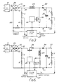
- FIG. 3 of the drawings shows a switched-mode power supply utilising one form of pre-regulator circuit in accordance with the present invention.
- the power supply comprises a full wave rectifier circuit 10 connected to an AC supply 11.
- the pre-regulator circuit referenced generally at 20, includes a positive supply line 21 connected to the positive output terminal 12 of the rectifier circuit and a negative supply line 22 connected to the negative output terminal 13 of the rectifier circuit.
- the negative supply line includes a sense resistor 9, the voltage developing across this resistor 9 being representative of the instantaneous current through an inductor 23.
- the positive supply line 21 includes the inductor 23 and a diode 24 arranged in series, a capacitor 25 being connected between the supply lines on the output side of the diode.
- a semiconductor power switch in the form of a switching transistor 26, is connected across the diode and the capacitor, as shown, and, as in the case of the circuit illustrated in the afore-mentioned European Patent Application No. 0059053, the inductor current rises if the switch is in the "closed", conductive condition and falls if the switch is in the "open", non-conductive condition.
- Operation of the switch is regulated by a control circuit, shown generally at 27, which is coupled to the switch via a suitable drive circuit 28, and, by this means, the inductor current and hence also the input current is constrained to follow the rectified sinusoidal wave form of the input voltage thereby to maintain the power factor of the circuit substantially at unity.
- a control circuit shown generally at 27, which is coupled to the switch via a suitable drive circuit 28, and, by this means, the inductor current and hence also the input current is constrained to follow the rectified sinusoidal wave form of the input voltage thereby to maintain the power factor of the circuit substantially at unity.
- control circuit 27 includes a comparison circuit 40 which is arranged to function as a Schmitt trigger with variable hysteresis and, in effect, defines the upper and lower bounds of a control band within which the input current is permitted to vary.
- the control band closely follows, and in this example is centred on, a sinusoidal reference signal which is derived from, and is proportional to, the input voltage.
- the inductor current is constrained to vary as a rectified sine wave, in phase with the input voltage, and exhibits a high frequency saw tooth modulation due to the action of the switch.
- the action of the control means is directly determined by a comparison of the inductor current with the upper and lower bounds of the control band, no comparison for dynamic or accumulative error is required and the control system is largely unaffected by circuitry elements.
- the high frequency saw tooth ripple in the inductor current will be removed however by a low pass radio frequency interference filter 29 on the AC side of the rectifier 10 which results in a sinusoidal input current being drawn from the AC supply.
- the comparison circuit of the present invention is so arranged that the width of the control band, defined by the upper and lower bounds, can be varied thereby to effect control over the frequency of the saw tooth modulation. More specifically, the width of the control band may be varied, during operation, to maintain the modulation frequency at a fixed value, or within a narrow range of values, irrespective of variations of one or more operational parameters of the pre-regulator circuit (e.g. load current, load voltage, supply frequency) and/or of an external circuit with which the pre-regulator circuit is operationally associated.
- the width of the control band may be varied, during operation, to maintain the modulation frequency at a fixed value, or within a narrow range of values, irrespective of variations of one or more operational parameters of the pre-regulator circuit (e.g. load current, load voltage, supply frequency) and/or of an external circuit with which the pre-regulator circuit is operationally associated.
- the control circuit 27 consists of the comparison circuit in the form of a variable hysteresis Schmitt trigger 40, an error amplifier 41 two multipliers 42, 43 and an inverting amplifier 47.
- the Schmitt trigger is arranged to switch states dependent on the values of a reference voltage V KI and a hysteresis voltage V H each derived from the values of the input and output voltages V I , V O indicated in Figure 3 via respective resistive potential divider arrangements 5, 6 and 7, 8, together with the value of a voltage V C representative of the inductor current.
- the variable hysteresis Schmitt trigger 40 is formed from two voltage comparators 49, 51 a voltage adder 53, a voltage subtractor 55 and a Reset-Set (RS) flip flop 57.
- the hysteresis signal, V H is added to and subtracted from the rectified sinusoidal reference signal V KI to give the two reference voltages in V+, V ⁇ . These two voltages are applied to the two voltage comparators 49, 51, forming the upper and lower bounds of the control band envelope.
- the voltage V C developed across the sense resistor 9, and thus representative of the instantaneous current through the inductor, is applied to the other comparator terminals.
- the output of the RS flip flop 57 drives the power switch 26 via a buffer circuit indicated as 59.
- the Set and Reset inputs of the flip flop 57 are controlled by the outputs of the comparators 49, 51.
- the inductor current increases with V C increasing proportionately until it reaches the upper voltage bound, V+.
- the output of comparator 49 then flips to logic 1 causing the flip flop 57 to reset to a logic 0, thus turning the power switch off.
- the inductor current then falls, causing a proportional reduction in the signal V C .
- V C falls to the lower bound V ⁇
- the output of comparator 51 flips to logic 1, setting the RS flip flop 57 and turning the power switch on. The cycle then repeats.
- the voltage signal V C which is directly proportional to the inductor current is conditioned by the inverting amplifier 47 so that it of the correct magnitude and polarity to be compared with in V+ and V ⁇ .
- the reference signal V KI is proportional to the input voltage signal V I , the constant of proportionality being determined by the error amplifier 41 and multiplier 43.
- the error amplifier 41 compares the output voltage sense signal, V O with a stable voltage reference V REF .
- the error amplifier 41 has a high gain low pass response, with a cut off frequency significantly below the supply frequency, this resulting in a DC voltage output from the error amplifier 41 whose magnitude is dependent on the load current and load voltage.
- the voltage multiplier 43 completes the output voltage control feedback loop, calculating the product of the rectified sinusoidal signal V I and the DC output from the error ampliflier 41.
- the load voltage is regulated such that it is largely constant, i.e. independent of load current and supply voltage.
- the response of the error amplifier 41 must necessarily be slow and a separate fast acting protection circuit (not shown) will be required to avoid large transient voltages across the output if the load is suddenly released. Such an over voltage protection circuit will inhibit the output of the buffer circuit 59 whenever the output voltage exceeds a nominal voltage by a suitable margin.
- V H The hysteresis signal, V H is derived from the analog voltage multiplier 42.
- This algorithm ensures a nearly constant switching frequency, whose absolute value is inversely proportional to the constant K.
- FIG. 5 illustrates an alternative control system to that shown in Figure 4, designed to give superior control at lower powers whilst maintaining accurate frequency control.
- Most features of the alternative control system are equivalent to those shown in Figure 4 and are thus correspondingly labelled.
- the Schmitt trigger circuit 60 differs from that shown in Figure 4 however in that the substractor 55 which is used in the first control system to produce a value of the lower voltage bound V ⁇ , together with the associated comparator 51 are replaced by a monostable 61 arranged to produce pulses at time intervals proportional to the value of the input voltage V I .
- the upper voltage bound V+ is again defined by the addition of the reference signal V KI and the hysteresis signal V H .
- the lower voltage bound V ⁇ is however replaced by the use of an off time proportional to V I .
- the period (shown in Figure 2 as F′) for which the switch 26 is 'on' may also be controlled using a timer system.
- the circuit shown in Figure 3 is known as a step-up, or boost regulator circuit since, with the power switch connected between the supply lines, the input current rises when the switch is closed and falls when the switch is open.
- the present invention is also applicable to another kind of pre-regulator circuit, shown in Figure 6, which is known is the buck boost regulator circuit.
- This form of regulator circuit differs from the step up or boost regulator circuit in that power switch 26 is connected into the positive supply line and the inductor 23 is connected between the power lines. With this arrangement, the input current rises when the switch is open and falls when the switch is closed.
- the form and operation of the two alternative controls circuits shown in Figures 4 and 5 will in principle, however, be the same as that for the step-up or boost regulator.
- the control algorithms will differ from those in the step-up converter.
- the buck boost converter input current is not a smoothed form of the inductor current. Current is drawn from the input only when the power switch is turned on.
- the inductor current must be centered around a reference signal given by,
- the hysteresis voltage is given by, where K′ and K ⁇ are constants.
- switched-mode regulator circuits in accordance with the invention described herebefore find particular application in the drive circuits of gaseous discharge lamps. Circuits in accordance with the invention will also find application however in other situations where a load, for example a motor or a television, driven from an AC supply requires an intermediate DC voltage, and it is required that the circuit presents a load on the power supply which is substantially of unity power factor.
Landscapes
- Engineering & Computer Science (AREA)
- Power Engineering (AREA)
- Dc-Dc Converters (AREA)
- Rectifiers (AREA)
Applications Claiming Priority (2)
| Application Number | Priority Date | Filing Date | Title |
|---|---|---|---|
| GB8905177 | 1989-03-07 | ||
| GB898905177A GB8905177D0 (en) | 1989-03-07 | 1989-03-07 | Switched-mode regulator circuit |
Publications (2)
| Publication Number | Publication Date |
|---|---|
| EP0386980A2 true EP0386980A2 (de) | 1990-09-12 |
| EP0386980A3 EP0386980A3 (de) | 1990-10-17 |
Family
ID=10652874
Family Applications (1)
| Application Number | Title | Priority Date | Filing Date |
|---|---|---|---|
| EP19900302326 Withdrawn EP0386980A3 (de) | 1989-03-07 | 1990-03-05 | Schaltungsmode-Reglerschaltung |
Country Status (5)
| Country | Link |
|---|---|
| EP (1) | EP0386980A3 (de) |
| JP (1) | JPH0340752A (de) |
| AU (1) | AU5076790A (de) |
| CA (1) | CA2011492A1 (de) |
| GB (1) | GB8905177D0 (de) |
Cited By (16)
| Publication number | Priority date | Publication date | Assignee | Title |
|---|---|---|---|---|
| GB2253311A (en) * | 1991-02-27 | 1992-09-02 | Astec Int Ltd | Power factor correction converter |
| DE4232829A1 (de) * | 1992-09-30 | 1994-03-31 | Siemens Nixdorf Inf Syst | Schaltungsanordnung zum Erzeugen einer Gleichspannung |
| FR2702606A1 (fr) * | 1993-03-09 | 1994-09-16 | Motorola Semiconducteurs | Alimentation électrique à découpage. |
| NL9400580A (nl) * | 1993-04-13 | 1994-11-01 | Samsung Electronics Co Ltd | Vermogenstoevoersysteem met een hoge vermogensfactor. |
| EP0582813A3 (de) * | 1992-08-10 | 1994-12-21 | Ibm | Im kritischen Bereich kontinuierlich arbeitender Verstärkungswandler. |
| EP0593257A3 (de) * | 1992-10-12 | 1995-02-01 | Nemic Lambda Kk | Verstärkerwandler. |
| EP0650250A1 (de) * | 1993-10-22 | 1995-04-26 | STMicroelectronics S.r.l. | Gleichstromwandler im diskontinuierlichem Betrieb arbeitend |
| EP0780751A3 (de) * | 1995-12-22 | 1998-05-20 | Motorola Semiconducteurs S.A. | Leistungsfaktor-Steuerschaltung |
| AT403865B (de) * | 1991-07-10 | 1998-06-25 | Fronius Schweissmasch | Spannungsumsetzungsvorrichtung für einen gleichspannungsverbraucher |
| EP1411622A3 (de) * | 2002-10-14 | 2006-01-18 | Nicotech Limited | Umrichterschaltungen |
| WO2008022656A1 (en) * | 2006-08-25 | 2008-02-28 | Tte Germany Gmbh | Switched mode power supply |
| CN102187559A (zh) * | 2008-11-25 | 2011-09-14 | 株式会社村田制作所 | Pfc变换器 |
| CN102484425A (zh) * | 2009-09-11 | 2012-05-30 | 株式会社村田制作所 | Pfc转换器 |
| WO2016090232A1 (en) * | 2014-12-05 | 2016-06-09 | General Electric Company | Power conversion system |
| CN106537750A (zh) * | 2014-08-05 | 2017-03-22 | 三菱电机株式会社 | 电力转换装置 |
| IT202000006976A1 (it) * | 2020-04-02 | 2021-10-02 | St Microelectronics Srl | Procedimento di controllo di un convertitore switching a frequenza variabile, e corrispondente apparecchiatura di convertitore a frequenza variabile |
Families Citing this family (5)
| Publication number | Priority date | Publication date | Assignee | Title |
|---|---|---|---|---|
| WO1992004808A1 (en) * | 1990-08-31 | 1992-03-19 | Siew Ean Wong | Improvements in electronic ballasts |
| US5426344B1 (en) * | 1990-08-31 | 1996-12-31 | Ultralite International Pty Li | Electronic ballasts |
| US5289361A (en) * | 1991-01-16 | 1994-02-22 | Vlt Corporation | Adaptive boost switching preregulator and method |
| US6746725B2 (en) | 2000-08-31 | 2004-06-08 | 3M Innovative Properties Company | Acrylic foam pressure sensitive adhesive method thereof |
| US8536850B2 (en) * | 2010-09-13 | 2013-09-17 | Immense Advance Technology Corp. | High side controller capable of sensing input voltage and ouput voltage of a power conversion circuit |
Family Cites Families (2)
| Publication number | Priority date | Publication date | Assignee | Title |
|---|---|---|---|---|
| EP0059053A3 (de) * | 1981-02-21 | 1983-05-18 | THORN EMI plc | Getakteter Schaltnetzteil |
| US4437146A (en) * | 1982-08-09 | 1984-03-13 | Pacific Electro Dynamics, Inc. | Boost power supply having power factor correction circuit |
-
1989
- 1989-03-07 GB GB898905177A patent/GB8905177D0/en active Pending
-
1990
- 1990-03-05 EP EP19900302326 patent/EP0386980A3/de not_active Withdrawn
- 1990-03-05 CA CA002011492A patent/CA2011492A1/en not_active Abandoned
- 1990-03-06 JP JP2052896A patent/JPH0340752A/ja active Pending
- 1990-03-07 AU AU50767/90A patent/AU5076790A/en not_active Abandoned
Cited By (21)
| Publication number | Priority date | Publication date | Assignee | Title |
|---|---|---|---|---|
| US5349284A (en) * | 1991-02-27 | 1994-09-20 | Astec International, Ltd. | Power factor boost converter power supply |
| GB2253311A (en) * | 1991-02-27 | 1992-09-02 | Astec Int Ltd | Power factor correction converter |
| AT403865B (de) * | 1991-07-10 | 1998-06-25 | Fronius Schweissmasch | Spannungsumsetzungsvorrichtung für einen gleichspannungsverbraucher |
| EP0582813A3 (de) * | 1992-08-10 | 1994-12-21 | Ibm | Im kritischen Bereich kontinuierlich arbeitender Verstärkungswandler. |
| DE4232829A1 (de) * | 1992-09-30 | 1994-03-31 | Siemens Nixdorf Inf Syst | Schaltungsanordnung zum Erzeugen einer Gleichspannung |
| EP0593257A3 (de) * | 1992-10-12 | 1995-02-01 | Nemic Lambda Kk | Verstärkerwandler. |
| FR2702606A1 (fr) * | 1993-03-09 | 1994-09-16 | Motorola Semiconducteurs | Alimentation électrique à découpage. |
| NL9400580A (nl) * | 1993-04-13 | 1994-11-01 | Samsung Electronics Co Ltd | Vermogenstoevoersysteem met een hoge vermogensfactor. |
| EP0650250A1 (de) * | 1993-10-22 | 1995-04-26 | STMicroelectronics S.r.l. | Gleichstromwandler im diskontinuierlichem Betrieb arbeitend |
| US5612610A (en) * | 1993-10-22 | 1997-03-18 | Sgs-Thomson Microelectronics S.R.L | DC-to-DC converter operating in a discontinuous mode |
| EP0780751A3 (de) * | 1995-12-22 | 1998-05-20 | Motorola Semiconducteurs S.A. | Leistungsfaktor-Steuerschaltung |
| EP1411622A3 (de) * | 2002-10-14 | 2006-01-18 | Nicotech Limited | Umrichterschaltungen |
| WO2008022656A1 (en) * | 2006-08-25 | 2008-02-28 | Tte Germany Gmbh | Switched mode power supply |
| CN102187559A (zh) * | 2008-11-25 | 2011-09-14 | 株式会社村田制作所 | Pfc变换器 |
| CN102187559B (zh) * | 2008-11-25 | 2014-07-30 | 株式会社村田制作所 | Pfc变换器 |
| CN102484425A (zh) * | 2009-09-11 | 2012-05-30 | 株式会社村田制作所 | Pfc转换器 |
| CN106537750A (zh) * | 2014-08-05 | 2017-03-22 | 三菱电机株式会社 | 电力转换装置 |
| CN106537750B (zh) * | 2014-08-05 | 2019-08-20 | 三菱电机株式会社 | 电力转换装置 |
| WO2016090232A1 (en) * | 2014-12-05 | 2016-06-09 | General Electric Company | Power conversion system |
| IT202000006976A1 (it) * | 2020-04-02 | 2021-10-02 | St Microelectronics Srl | Procedimento di controllo di un convertitore switching a frequenza variabile, e corrispondente apparecchiatura di convertitore a frequenza variabile |
| US11677316B2 (en) | 2020-04-02 | 2023-06-13 | Stmicroelectronics S.R.L. | Method to control a variable frequency switching converter, and corresponding variable frequency converter apparatus |
Also Published As
| Publication number | Publication date |
|---|---|
| AU5076790A (en) | 1990-09-20 |
| JPH0340752A (ja) | 1991-02-21 |
| EP0386980A3 (de) | 1990-10-17 |
| GB8905177D0 (en) | 1989-04-19 |
| CA2011492A1 (en) | 1990-09-07 |
Similar Documents
| Publication | Publication Date | Title |
|---|---|---|
| EP0386980A2 (de) | Schaltungsmode-Reglerschaltung | |
| KR100431782B1 (ko) | 역률보정회로 | |
| US6215287B1 (en) | Power supply apparatus | |
| US4301497A (en) | Flyback converter control with feed forward | |
| US6980445B2 (en) | Power factor improving converter and control method thereof | |
| US8179703B2 (en) | Power factor correction converter | |
| JP3994953B2 (ja) | 力率改善回路 | |
| US6307361B1 (en) | Method and apparatus for regulating the input impedance of PWM converters | |
| US6882551B2 (en) | Switching power supply device | |
| US5644214A (en) | Power factor correction circuit | |
| US5646513A (en) | Dynamic loop compensator for continuous mode power converters | |
| US4013939A (en) | Multiple feedback control apparatus for power conditioning equipment | |
| US6177782B1 (en) | Circuit and method of controlling a regulator with an output feedback signal and devoid of an input feedforward signal | |
| GB2195842A (en) | Controller for a resonant converter | |
| US4644254A (en) | Switch controller having a regulating path and an auxiliary regulating path parallel thereto | |
| US6160385A (en) | Circuit configuration for producing a load-independent output voltage | |
| JP3570173B2 (ja) | 交流から直流を生成する装置に設けられる制御回路 | |
| JP2001086737A (ja) | 電源装置 | |
| JPH0522944A (ja) | 順変換装置 | |
| JPH02280670A (ja) | 電源装置 | |
| JPH10127046A (ja) | 昇圧形コンバータの制御回路 | |
| JPH04178170A (ja) | 力率改善形整流装置 | |
| JPH04359675A (ja) | スイッチング電源の制御回路 | |
| JPS5836590B2 (ja) | Dc/dcコンバ−タの制御方式 | |
| JPH0639366Y2 (ja) | 直流安定化電源装置 |
Legal Events
| Date | Code | Title | Description |
|---|---|---|---|
| PUAI | Public reference made under article 153(3) epc to a published international application that has entered the european phase |
Free format text: ORIGINAL CODE: 0009012 |
|
| PUAL | Search report despatched |
Free format text: ORIGINAL CODE: 0009013 |
|
| AK | Designated contracting states |
Kind code of ref document: A2 Designated state(s): AT BE CH DE DK ES FR GB GR IT LI LU NL SE |
|
| AK | Designated contracting states |
Kind code of ref document: A3 Designated state(s): AT BE CH DE DK ES FR GB GR IT LI LU NL SE |
|
| STAA | Information on the status of an ep patent application or granted ep patent |
Free format text: STATUS: THE APPLICATION HAS BEEN WITHDRAWN |
|
| 18W | Application withdrawn |
Withdrawal date: 19910218 |