EP0388075A2 - Kontakte für Halbleiter-Vorrichtungen - Google Patents
Kontakte für Halbleiter-Vorrichtungen Download PDFInfo
- Publication number
- EP0388075A2 EP0388075A2 EP90302447A EP90302447A EP0388075A2 EP 0388075 A2 EP0388075 A2 EP 0388075A2 EP 90302447 A EP90302447 A EP 90302447A EP 90302447 A EP90302447 A EP 90302447A EP 0388075 A2 EP0388075 A2 EP 0388075A2
- Authority
- EP
- European Patent Office
- Prior art keywords
- integrated circuit
- regions
- insulating layer
- sloped
- layer
- Prior art date
- Legal status (The legal status is an assumption and is not a legal conclusion. Google has not performed a legal analysis and makes no representation as to the accuracy of the status listed.)
- Granted
Links
Images


Classifications
-
- H—ELECTRICITY
- H10—SEMICONDUCTOR DEVICES; ELECTRIC SOLID-STATE DEVICES NOT OTHERWISE PROVIDED FOR
- H10D—INORGANIC ELECTRIC SEMICONDUCTOR DEVICES
- H10D84/00—Integrated devices formed in or on semiconductor substrates that comprise only semiconducting layers, e.g. on Si wafers or on GaAs-on-Si wafers
- H10D84/80—Integrated devices formed in or on semiconductor substrates that comprise only semiconducting layers, e.g. on Si wafers or on GaAs-on-Si wafers characterised by the integration of at least one component covered by groups H10D12/00 or H10D30/00, e.g. integration of IGFETs
- H10D84/82—Integrated devices formed in or on semiconductor substrates that comprise only semiconducting layers, e.g. on Si wafers or on GaAs-on-Si wafers characterised by the integration of at least one component covered by groups H10D12/00 or H10D30/00, e.g. integration of IGFETs of only field-effect components
- H10D84/83—Integrated devices formed in or on semiconductor substrates that comprise only semiconducting layers, e.g. on Si wafers or on GaAs-on-Si wafers characterised by the integration of at least one component covered by groups H10D12/00 or H10D30/00, e.g. integration of IGFETs of only field-effect components of only insulated-gate FETs [IGFET]
-
- H—ELECTRICITY
- H10—SEMICONDUCTOR DEVICES; ELECTRIC SOLID-STATE DEVICES NOT OTHERWISE PROVIDED FOR
- H10D—INORGANIC ELECTRIC SEMICONDUCTOR DEVICES
- H10D30/00—Field-effect transistors [FET]
- H10D30/01—Manufacture or treatment
- H10D30/021—Manufacture or treatment of FETs having insulated gates [IGFET]
- H10D30/0223—Manufacture or treatment of FETs having insulated gates [IGFET] having source and drain regions or source and drain extensions self-aligned to sides of the gate
- H10D30/0227—Manufacture or treatment of FETs having insulated gates [IGFET] having source and drain regions or source and drain extensions self-aligned to sides of the gate having both lightly-doped source and drain extensions and source and drain regions self-aligned to the sides of the gate, e.g. lightly-doped drain [LDD] MOSFET or double-diffused drain [DDD] MOSFET
-
- H—ELECTRICITY
- H10—SEMICONDUCTOR DEVICES; ELECTRIC SOLID-STATE DEVICES NOT OTHERWISE PROVIDED FOR
- H10D—INORGANIC ELECTRIC SEMICONDUCTOR DEVICES
- H10D30/00—Field-effect transistors [FET]
- H10D30/60—Insulated-gate field-effect transistors [IGFET]
-
- H—ELECTRICITY
- H10—SEMICONDUCTOR DEVICES; ELECTRIC SOLID-STATE DEVICES NOT OTHERWISE PROVIDED FOR
- H10D—INORGANIC ELECTRIC SEMICONDUCTOR DEVICES
- H10D64/00—Electrodes of devices having potential barriers
- H10D64/20—Electrodes characterised by their shapes, relative sizes or dispositions
- H10D64/23—Electrodes carrying the current to be rectified, amplified, oscillated or switched, e.g. sources, drains, anodes or cathodes
- H10D64/251—Source or drain electrodes for field-effect devices
- H10D64/258—Source or drain electrodes for field-effect devices characterised by the relative positions of the source or drain electrodes with respect to the gate electrode
-
- H—ELECTRICITY
- H10—SEMICONDUCTOR DEVICES; ELECTRIC SOLID-STATE DEVICES NOT OTHERWISE PROVIDED FOR
- H10P—GENERIC PROCESSES OR APPARATUS FOR THE MANUFACTURE OR TREATMENT OF DEVICES COVERED BY CLASS H10
- H10P76/00—Manufacture or treatment of masks on semiconductor bodies, e.g. by lithography or photolithography
- H10P76/40—Manufacture or treatment of masks on semiconductor bodies, e.g. by lithography or photolithography of masks comprising inorganic materials
-
- H—ELECTRICITY
- H10—SEMICONDUCTOR DEVICES; ELECTRIC SOLID-STATE DEVICES NOT OTHERWISE PROVIDED FOR
- H10P—GENERIC PROCESSES OR APPARATUS FOR THE MANUFACTURE OR TREATMENT OF DEVICES COVERED BY CLASS H10
- H10P95/00—Generic processes or apparatus for manufacture or treatments not covered by the other groups of this subclass
-
- H—ELECTRICITY
- H10—SEMICONDUCTOR DEVICES; ELECTRIC SOLID-STATE DEVICES NOT OTHERWISE PROVIDED FOR
- H10W—GENERIC PACKAGES, INTERCONNECTIONS, CONNECTORS OR OTHER CONSTRUCTIONAL DETAILS OF DEVICES COVERED BY CLASS H10
- H10W20/00—Interconnections in chips, wafers or substrates
- H10W20/01—Manufacture or treatment
- H10W20/071—Manufacture or treatment of dielectric parts thereof
- H10W20/081—Manufacture or treatment of dielectric parts thereof by forming openings in the dielectric parts
- H10W20/082—Manufacture or treatment of dielectric parts thereof by forming openings in the dielectric parts the openings being tapered via holes
-
- Y—GENERAL TAGGING OF NEW TECHNOLOGICAL DEVELOPMENTS; GENERAL TAGGING OF CROSS-SECTIONAL TECHNOLOGIES SPANNING OVER SEVERAL SECTIONS OF THE IPC; TECHNICAL SUBJECTS COVERED BY FORMER USPC CROSS-REFERENCE ART COLLECTIONS [XRACs] AND DIGESTS
- Y10—TECHNICAL SUBJECTS COVERED BY FORMER USPC
- Y10S—TECHNICAL SUBJECTS COVERED BY FORMER USPC CROSS-REFERENCE ART COLLECTIONS [XRACs] AND DIGESTS
- Y10S257/00—Active solid-state devices, e.g. transistors, solid-state diodes
- Y10S257/90—MOSFET type gate sidewall insulating spacer
Definitions
- the present invention relates generally to semiconductor integrated circuit processing, and more specifically to improving step coverages for metal signal lines at contacts and other locations.
- the Sakamoto reference shows the use of polysilicon regions disposed over active area contacts, with smaller contact openings in a glass layer through which the metal makes contact with such polysilicon regions.
- the Lau reference shows the use of selective silicon growth epitaxy to form enlarged areas which make contact with tungsten plugs.
- the tungsten plugs are fabricated in relatively small contact openings through a BPSG glass layer.
- Steep sided contact cuts especially in contact openings having a small cross-sectional area, can lead to the formation of voids within the contact opening, and incomplete contact coverage. This degrades the electrical characteristics of the metal to silicon contact.
- a related problem is metal step coverage over polysilicon signal lines.
- the metal traces tend to be thinner at the edges of such steps, leading to electromigration problems, especially in the smaller geometries.
- sidewall oxide spacers are formed.
- An insulating glass layer is formed over the surface of the integrated circuit, and reflow of such glass layer is performed.
- the glass insulating layer is etched back using an anisotropic etch, glass filler regions are left along the sidewalls of contact openings and along steps. These filler regions cause the insulator profile over steps and in contact openings to be less steeply sloped, providing better metal coverage in these regions.
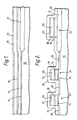
- FIGS. 1-6 represent a cross-section of a portion of an integrated circuit during fabrication. The figures are not drawn to scale, but instead are drawn so as to illustrate the important features of the invention.
- an integrated circuit is to be formed in a substrate 10 .
- Selected regions of the substrate 10 are oxidized to form a field oxide 12 as known in the art.
- Active devices are formed in those portions of the substrate 10 not covered by field oxide 12 .
- a gate oxide layer 14 is grown over the active regions.
- a layer of polycrystalline silicon 16 is then deposited over the entire surface of the chip. This layer 16 will be patterned to form device gates and interconnect lines.
- a silicide layer 18 such as tantalum disilicide (TaSi2) or titanium disilicide (TiSi2) is preferably formed over the polycrystalline silicon layer 18 in order to decrease resistivity
- a layer of oxide 20 is deposited using chemical vapor deposition (CVD), followed by formation of a nitride layer 22 (Si3N4), which is also preferably formed using a CVD process.
- CVD chemical vapor deposition
- Si3N4 nitride layer 22
- each transistor gate region 24 consists of a gate oxide-polysilicon/silicide-oxide-nitride stack.
- Interconnect regions 26 are similar, without the gate oxide layers 14 .
- lightly doped regions 28 are created by ion implant. These regions 28 are used to form lightly doped drain (LDD) structures as known in the art.
- LDD lightly doped drain
- LTO undoped low temperature ode
- the LTO layer 30 is etched back using an anisotropic plasma etch, resulting in sidewall spacers 32 alongside gates 24 and interconnect 26 as known in the art.
- Heavily doped source/drain regions 34 are then formed by ion implantation and anneal as known in the art.
- a layer 36 of phospho-silicate glass (PSG) or boro-phospho-silicate glass (BPSG) is formed over the integrated circuit.
- the BPSG layer 36 substantially conforms with the topography of underlying device.
- the BPSG layer 36 is heated to reflow, smoothing out the surface thereof.
- the BPSG layer 36 is etched back using an anisotropic plasma etch, resulting in the formation of filler regions 38 alongside steep sidewalls such as those formed by sidewall spacers 32 .
- the nitride layer 22 acts as an etch stop for the BPSG layer 36 in order to protect gates 24 and interconnect regions 26 .
- Reflow of the BPSG layer 36 prior to etch back causes the filler regions 38 to have a relatively gently sloped cross-section. If the BPSG layer 36 is etched back without reflow, the filler regions 38 tend to have a steeper cross-section similar to that of the sidewall spacers 32 .
- barrier metal 40 such as titanium-tungsten TiW
- a layer 42 of a metal such as aluminum.
- the metal layer 42 makes contact with the source/drain regions 34 through the barrier metal layer 40 .
- an interconnect contact region 44 can be defined prior to the deposition of metal layers 40 and 42 .
- Aluminum interconnect layer 42 is then patterned and passivated as known in the art, followed by deposition and patterning of additional metal layers if desired.
- the filler regions 38 smooth the profile of contacts to the source/drain regions 34 , and the steps over interconnect regions 26 .
- These fillers 38 change the cross-sectional profile of steps from nearly vertical to a more gently sloped profile. This allows the metal to be deposited with a greatly decreased chance of void formation or incomplete contact formation.
- the gate oxide layer 14 will be grown to a depth of approximately 400 to 800 angstroms.
- the polycrystalline silicon layer 16 will typically be approximately 1,500 angstroms thick, and the silicide layer 18 , if used, is typically from 1,000 to 1,500 angstroms thick.
- the oxide layer 20 is preferably from 2,000 to 6,000 angstroms thick, while the nitride layer 22 has a thickness of approximately 500 to 1,000 angstroms.
- the LTO ode layer 30 used to form the sidewall spacers 32 preferably has a depth of approximately 1,500 angstroms prior to etch back.
- the BPSG layer 36 is preferably deposited to a depth of approximately 5,000 angstroms prior to reflow. Of course, after reflow the thickness will vary somewhat according to the underlying topographical features.
- process steps described above can be used with nearly any conventional process flow.
- the described process steps are compatible with CMOS, NMOS, and bipolar/CMOS process flows.
Landscapes
- Internal Circuitry In Semiconductor Integrated Circuit Devices (AREA)
- Drying Of Semiconductors (AREA)
Applications Claiming Priority (2)
| Application Number | Priority Date | Filing Date | Title |
|---|---|---|---|
| US32458689A | 1989-03-16 | 1989-03-16 | |
| US324586 | 1989-03-16 |
Publications (3)
| Publication Number | Publication Date |
|---|---|
| EP0388075A2 true EP0388075A2 (de) | 1990-09-19 |
| EP0388075A3 EP0388075A3 (de) | 1991-01-02 |
| EP0388075B1 EP0388075B1 (de) | 1996-11-06 |
Family
ID=23264251
Family Applications (1)
| Application Number | Title | Priority Date | Filing Date |
|---|---|---|---|
| EP90302447A Expired - Lifetime EP0388075B1 (de) | 1989-03-16 | 1990-03-07 | Kontakte für Halbleiter-Vorrichtungen |
Country Status (5)
| Country | Link |
|---|---|
| US (1) | US5847465A (de) |
| EP (1) | EP0388075B1 (de) |
| JP (1) | JP2668089B2 (de) |
| KR (1) | KR0173458B1 (de) |
| DE (1) | DE69029046T2 (de) |
Cited By (6)
| Publication number | Priority date | Publication date | Assignee | Title |
|---|---|---|---|---|
| US5155057A (en) * | 1990-11-05 | 1992-10-13 | Micron Technology, Inc. | Stacked v-cell capacitor using a disposable composite dielectric on top of a digit line |
| DE4212494A1 (de) * | 1991-04-17 | 1992-10-22 | Mitsubishi Electric Corp | Verfahren zur bildung einer seitenwandisolierschicht und halbleitereinrichtung |
| US5219778A (en) * | 1990-10-16 | 1993-06-15 | Micron Technology, Inc. | Stacked V-cell capacitor |
| US5236855A (en) * | 1990-11-06 | 1993-08-17 | Micron Technology, Inc. | Stacked V-cell capacitor using a disposable outer digit line spacer |
| DE4232621C1 (de) * | 1992-09-29 | 1994-03-10 | Siemens Ag | Herstellverfahren für ein selbstjustiertes Kontaktloch und Halbleiterstruktur |
| US5301222A (en) * | 1990-01-24 | 1994-04-05 | Nec Corporation | Portable radio telephone set for generating pattern signals representative of alphanumeric letters indicative of a telephone number |
Families Citing this family (8)
| Publication number | Priority date | Publication date | Assignee | Title |
|---|---|---|---|---|
| TW421964B (en) * | 1996-08-28 | 2001-02-11 | Sanyo Electric Co | Image data encoding device |
| JP3114931B2 (ja) * | 1998-03-30 | 2000-12-04 | 日本電気株式会社 | 導電体プラグを備えた半導体装置およびその製造方法 |
| US6734564B1 (en) * | 1999-01-04 | 2004-05-11 | International Business Machines Corporation | Specially shaped contact via and integrated circuit therewith |
| KR100578120B1 (ko) * | 1999-09-13 | 2006-05-10 | 삼성전자주식회사 | 신뢰성 있는 비트라인 콘택 구조 및 이를 형성하는 방법 |
| KR100426811B1 (ko) * | 2001-07-12 | 2004-04-08 | 삼성전자주식회사 | 셀프얼라인 콘택을 갖는 반도체 소자 및 그의 제조방법 |
| US7306552B2 (en) * | 2004-12-03 | 2007-12-11 | Samsung Electronics Co., Ltd. | Semiconductor device having load resistor and method of fabricating the same |
| KR100771537B1 (ko) * | 2005-11-21 | 2007-10-31 | 주식회사 하이닉스반도체 | 금속실리사이드막을 갖는 반도체소자의 제조방법 |
| EP3570317A1 (de) * | 2018-05-17 | 2019-11-20 | IMEC vzw | Flächenselektive abscheidung eines maskenmaterials |
Family Cites Families (16)
| Publication number | Priority date | Publication date | Assignee | Title |
|---|---|---|---|---|
| DE2040180B2 (de) * | 1970-01-22 | 1977-08-25 | Intel Corp, Mountain View, Calif. (V.St.A.) | Verfahren zur verhinderung von mechanischen bruechen einer duennen, die oberflaeche eines halbleiterkoerpers ueberdeckende isolierschichten ueberziehenden elektrisch leitenden schicht |
| CA1174285A (en) * | 1980-04-28 | 1984-09-11 | Michelangelo Delfino | Laser induced flow of integrated circuit structure materials |
| US4284659A (en) * | 1980-05-12 | 1981-08-18 | Bell Telephone Laboratories | Insulation layer reflow |
| US4455325A (en) * | 1981-03-16 | 1984-06-19 | Fairchild Camera And Instrument Corporation | Method of inducing flow or densification of phosphosilicate glass for integrated circuits |
| US4489481A (en) * | 1982-09-20 | 1984-12-25 | Texas Instruments Incorporated | Insulator and metallization method for VLSI devices with anisotropically-etched contact holes |
| JPS5984442A (ja) * | 1982-11-04 | 1984-05-16 | Nec Corp | 半導体装置の製造方法 |
| AU563771B2 (en) * | 1983-12-08 | 1987-07-23 | Amalgamated Wireless (Australasia) Limited | Fabrication of integrated circuits |
| JPS6116571A (ja) * | 1984-07-03 | 1986-01-24 | Ricoh Co Ltd | 半導体装置の製造方法 |
| US4641420A (en) * | 1984-08-30 | 1987-02-10 | At&T Bell Laboratories | Metalization process for headless contact using deposited smoothing material |
| JPS61183952A (ja) * | 1985-02-09 | 1986-08-16 | Fujitsu Ltd | 半導体記憶装置及びその製造方法 |
| US4808548A (en) * | 1985-09-18 | 1989-02-28 | Advanced Micro Devices, Inc. | Method of making bipolar and MOS devices on same integrated circuit substrate |
| US4755479A (en) * | 1986-02-17 | 1988-07-05 | Fujitsu Limited | Manufacturing method of insulated gate field effect transistor using reflowable sidewall spacers |
| US4795718A (en) * | 1987-05-12 | 1989-01-03 | Harris Corporation | Self-aligned contact for MOS processing |
| US4786609A (en) * | 1987-10-05 | 1988-11-22 | North American Philips Corporation, Signetics Division | Method of fabricating field-effect transistor utilizing improved gate sidewall spacers |
| KR930020669A (ko) * | 1992-03-04 | 1993-10-20 | 김광호 | 고집적 반도체장치 및 그 제조방법 |
| JPH05315623A (ja) * | 1992-05-08 | 1993-11-26 | Nippon Steel Corp | 不揮発性半導体記憶装置 |
-
1990
- 1990-03-07 DE DE69029046T patent/DE69029046T2/de not_active Expired - Fee Related
- 1990-03-07 EP EP90302447A patent/EP0388075B1/de not_active Expired - Lifetime
- 1990-03-12 KR KR1019900003293A patent/KR0173458B1/ko not_active Expired - Fee Related
- 1990-03-15 JP JP2066720A patent/JP2668089B2/ja not_active Expired - Fee Related
-
1995
- 1995-05-08 US US08/436,165 patent/US5847465A/en not_active Expired - Lifetime
Cited By (10)
| Publication number | Priority date | Publication date | Assignee | Title |
|---|---|---|---|---|
| US5301222A (en) * | 1990-01-24 | 1994-04-05 | Nec Corporation | Portable radio telephone set for generating pattern signals representative of alphanumeric letters indicative of a telephone number |
| US5219778A (en) * | 1990-10-16 | 1993-06-15 | Micron Technology, Inc. | Stacked V-cell capacitor |
| US5155057A (en) * | 1990-11-05 | 1992-10-13 | Micron Technology, Inc. | Stacked v-cell capacitor using a disposable composite dielectric on top of a digit line |
| US5236855A (en) * | 1990-11-06 | 1993-08-17 | Micron Technology, Inc. | Stacked V-cell capacitor using a disposable outer digit line spacer |
| DE4212494A1 (de) * | 1991-04-17 | 1992-10-22 | Mitsubishi Electric Corp | Verfahren zur bildung einer seitenwandisolierschicht und halbleitereinrichtung |
| US5432367A (en) * | 1991-04-17 | 1995-07-11 | Mitsubishi Denki Kabushiki Kaisha | Semiconductor device having sidewall insulating film |
| US5541127A (en) * | 1991-04-17 | 1996-07-30 | Mitsubishi Denki Kabushiki Kaisha | Manufacturing method of sidewall insulating film |
| DE4232621C1 (de) * | 1992-09-29 | 1994-03-10 | Siemens Ag | Herstellverfahren für ein selbstjustiertes Kontaktloch und Halbleiterstruktur |
| US5432381A (en) * | 1992-09-29 | 1995-07-11 | Siemens Aktiengesellschaft | Manufacturing method for a self-aligned through hole and semiconductor structure |
| US5460690A (en) * | 1992-09-29 | 1995-10-24 | Siemens Aktiengesellschaft | Manufacturing method for a self-aligned through hole and semiconductor structure |
Also Published As
| Publication number | Publication date |
|---|---|
| DE69029046T2 (de) | 1997-03-06 |
| KR0173458B1 (ko) | 1999-02-01 |
| JP2668089B2 (ja) | 1997-10-27 |
| US5847465A (en) | 1998-12-08 |
| DE69029046D1 (de) | 1996-12-12 |
| EP0388075A3 (de) | 1991-01-02 |
| KR900015342A (ko) | 1990-10-26 |
| JPH02280327A (ja) | 1990-11-16 |
| EP0388075B1 (de) | 1996-11-06 |
Similar Documents
| Publication | Publication Date | Title |
|---|---|---|
| EP1532679B1 (de) | Selbstausrichtende kontakte für gates | |
| EP0542477B1 (de) | Verfahren zur Herstellung einer integrierten Schaltung mit selbstjustierten Kontakten zwischen eng beabstandeten Strukturen | |
| US4987099A (en) | Method for selectively filling contacts or vias or various depths with CVD tungsten | |
| EP0088922B1 (de) | Verfahren zum Herstellen von Elektroden und Verdrahtungsstreifen auf einer Halbleiteranordnung | |
| US6737310B2 (en) | Self-aligned process for a stacked gate RF MOSFET device | |
| EP0540446B1 (de) | Selbstjustierende Kontaktstützer für Halbleitervorrichtungen | |
| US6180475B1 (en) | Transistor formation with local interconnect overetch immunity | |
| US5981383A (en) | Method of fabricating a salicide layer of a device electrode | |
| JPH0797571B2 (ja) | 半導体構造体にコンタクトウインド−を形成する方法 | |
| EP0388075B1 (de) | Kontakte für Halbleiter-Vorrichtungen | |
| US5073510A (en) | Fabrication method of contact window in semiconductor device | |
| US4933297A (en) | Method for etching windows having different depths | |
| US4822754A (en) | Fabrication of FETs with source and drain contacts aligned with the gate electrode | |
| EP0404372B1 (de) | Verfahren zur Herstellung von polykristallinen Siliziumkontakten | |
| US5380671A (en) | Method of making non-trenched buried contact for VLSI devices | |
| US5747367A (en) | Multi-level transistor fabrication method with high performance source/drain connection | |
| EP0700081A2 (de) | Verfahren zur Herstellung einer Halbleiteranordnung mit integrierten Schaltungen unter Verwendung selbst-alignierter Silizid-Kontakte für die Zonen | |
| US6054385A (en) | Elevated local interconnect and contact structure | |
| EP0526244B1 (de) | Verfahren zur Herstellung eines vergrabenen Kontaktes aus Polysilizium | |
| JPH1187529A (ja) | 集積回路コンタクト | |
| US5589418A (en) | Method of forming a polysilicon buried contact | |
| US6211046B1 (en) | Method of manufacturing a semiconductor device | |
| US6812142B1 (en) | Method and interlevel dielectric structure for improved metal step coverage | |
| US6080647A (en) | Process to form a trench-free buried contact | |
| US5146309A (en) | Method for forming polycrystalline silicon contacts |
Legal Events
| Date | Code | Title | Description |
|---|---|---|---|
| PUAI | Public reference made under article 153(3) epc to a published international application that has entered the european phase |
Free format text: ORIGINAL CODE: 0009012 |
|
| AK | Designated contracting states |
Kind code of ref document: A2 Designated state(s): DE FR GB IT |
|
| PUAL | Search report despatched |
Free format text: ORIGINAL CODE: 0009013 |
|
| AK | Designated contracting states |
Kind code of ref document: A3 Designated state(s): DE FR GB IT |
|
| 17P | Request for examination filed |
Effective date: 19910316 |
|
| 17Q | First examination report despatched |
Effective date: 19930517 |
|
| GRAG | Despatch of communication of intention to grant |
Free format text: ORIGINAL CODE: EPIDOS AGRA |
|
| GRAH | Despatch of communication of intention to grant a patent |
Free format text: ORIGINAL CODE: EPIDOS IGRA |
|
| GRAH | Despatch of communication of intention to grant a patent |
Free format text: ORIGINAL CODE: EPIDOS IGRA |
|
| GRAH | Despatch of communication of intention to grant a patent |
Free format text: ORIGINAL CODE: EPIDOS IGRA |
|
| GRAA | (expected) grant |
Free format text: ORIGINAL CODE: 0009210 |
|
| AK | Designated contracting states |
Kind code of ref document: B1 Designated state(s): DE FR GB IT |
|
| ITF | It: translation for a ep patent filed | ||
| REF | Corresponds to: |
Ref document number: 69029046 Country of ref document: DE Date of ref document: 19961212 |
|
| ET | Fr: translation filed | ||
| PLBE | No opposition filed within time limit |
Free format text: ORIGINAL CODE: 0009261 |
|
| STAA | Information on the status of an ep patent application or granted ep patent |
Free format text: STATUS: NO OPPOSITION FILED WITHIN TIME LIMIT |
|
| 26N | No opposition filed | ||
| PGFP | Annual fee paid to national office [announced via postgrant information from national office to epo] |
Ref country code: DE Payment date: 19980313 Year of fee payment: 9 |
|
| PG25 | Lapsed in a contracting state [announced via postgrant information from national office to epo] |
Ref country code: DE Free format text: LAPSE BECAUSE OF NON-PAYMENT OF DUE FEES Effective date: 20000101 |
|
| REG | Reference to a national code |
Ref country code: GB Ref legal event code: IF02 |
|
| PGFP | Annual fee paid to national office [announced via postgrant information from national office to epo] |
Ref country code: GB Payment date: 20030305 Year of fee payment: 14 |
|
| PGFP | Annual fee paid to national office [announced via postgrant information from national office to epo] |
Ref country code: FR Payment date: 20030310 Year of fee payment: 14 |
|
| PG25 | Lapsed in a contracting state [announced via postgrant information from national office to epo] |
Ref country code: GB Free format text: LAPSE BECAUSE OF NON-PAYMENT OF DUE FEES Effective date: 20040307 |
|
| GBPC | Gb: european patent ceased through non-payment of renewal fee | ||
| PG25 | Lapsed in a contracting state [announced via postgrant information from national office to epo] |
Ref country code: FR Free format text: LAPSE BECAUSE OF NON-PAYMENT OF DUE FEES Effective date: 20041130 |
|
| REG | Reference to a national code |
Ref country code: FR Ref legal event code: ST |
|
| PG25 | Lapsed in a contracting state [announced via postgrant information from national office to epo] |
Ref country code: IT Free format text: LAPSE BECAUSE OF NON-PAYMENT OF DUE FEES Effective date: 20050307 |