EP0390507A2 - Circuit de décharge et de détection de ligne de bit - Google Patents
Circuit de décharge et de détection de ligne de bit Download PDFInfo
- Publication number
- EP0390507A2 EP0390507A2 EP90303266A EP90303266A EP0390507A2 EP 0390507 A2 EP0390507 A2 EP 0390507A2 EP 90303266 A EP90303266 A EP 90303266A EP 90303266 A EP90303266 A EP 90303266A EP 0390507 A2 EP0390507 A2 EP 0390507A2
- Authority
- EP
- European Patent Office
- Prior art keywords
- cell
- current source
- select lines
- transistors
- arrangement
- Prior art date
- Legal status (The legal status is an assumption and is not a legal conclusion. Google has not performed a legal analysis and makes no representation as to the accuracy of the status listed.)
- Granted
Links
Images

Classifications
-
- G—PHYSICS
- G11—INFORMATION STORAGE
- G11C—STATIC STORES
- G11C7/00—Arrangements for writing information into, or reading information out from, a digital store
- G11C7/12—Bit line control circuits, e.g. drivers, boosters, pull-up circuits, pull-down circuits, precharging circuits, equalising circuits, for bit lines
-
- G—PHYSICS
- G11—INFORMATION STORAGE
- G11C—STATIC STORES
- G11C11/00—Digital stores characterised by the use of particular electric or magnetic storage elements; Storage elements therefor
- G11C11/21—Digital stores characterised by the use of particular electric or magnetic storage elements; Storage elements therefor using electric elements
- G11C11/34—Digital stores characterised by the use of particular electric or magnetic storage elements; Storage elements therefor using electric elements using semiconductor devices
- G11C11/40—Digital stores characterised by the use of particular electric or magnetic storage elements; Storage elements therefor using electric elements using semiconductor devices using transistors
- G11C11/41—Digital stores characterised by the use of particular electric or magnetic storage elements; Storage elements therefor using electric elements using semiconductor devices using transistors forming static cells with positive feedback, i.e. cells not needing refreshing or charge regeneration, e.g. bistable multivibrator or Schmitt trigger
- G11C11/413—Auxiliary circuits, e.g. for addressing, decoding, driving, writing, sensing, timing or power reduction
- G11C11/414—Auxiliary circuits, e.g. for addressing, decoding, driving, writing, sensing, timing or power reduction for memory cells of the bipolar type
- G11C11/416—Read-write [R-W] circuits
Definitions
- This invention relates generally to a high-speed static memory array, and more particularly to a discharge and sensing circuit for a static memory array.
- the classic problem with sensing a bipolar random access memory is the high capacitance present along the bit lines.
- the total capacitance presented to the bit line is a function of the number of cells along the column to be read. Every cell along the column has at least one emitter tied to the bit line. So if 64 cells are tied to the column line, 64 emitters are tied to that column line. In most static memory cells, the emitter is heavily doped and the base is heavily doped, so that the emitter base capacitance is high. Assuming 64 cells on a column, 63 have reversed biased base-emitter junctions, resulting in very high bit line capacitance. All of this capacitance has to be charged and discharged to sense what is stored in a selected cell.
- a static memory cell includes two transistors which have opposite states. Reading the state of a given cell is a function of the sense circuit's ability to sense the voltage difference between bit lines tied to the emitters of the separate transistors which form a single cell. The only way to rapidly charge and discharge the capaci tance of the transistors tied to the bit line to sense the cell state is with current; the higher the current the faster rate of charge and discharge.
- the primary problem addressed by this invention is to provide a circuit arrangement and method for charging and discharging the capacitance tied to the bit lines very fast in order to maximize the speed with which a bipolar memory array can be read.
- two current sources are used, having a relatively small difference.
- the larger current source is used to discharge the capacitance on the bit line.
- only the difference between the two currents flows through the cell transistor being read.
- a high current flows in the bit line, but a much lower current in the cell.
- the voltages on the bases of the two transistors of the cell can be sensed directly, by diode followers connected to the emitters of the two transistors of the cell.
- diode followers connected to the emitters of the two transistors of the cell.
- a further problem with the prior art is the delay which results from the inability to sense the bit line directly; that is, in the prior art either a sense transistor or a differential amplifier is used on every column, and the system essentially senses the collector of the sense transistor or the differential amplifier and develops the differential signal at that point.
- This invention senses the nodes directly to get a direct reading of the voltage at the bit lines without the extra sense transistor or differential amplifier delay.
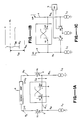
- FIGs 1A and 1B illustrate a typical bipolar static random access memory cell including a pair of cross coupled transistors Q1 and Q2.
- a pair of sense transistors Q3, Q4 are provided with their emitters 5, 6 connected to the emitters 7, 8 of the cross-coupled transistors Q1, Q2 in the cell.
- the voltage level of the base of one of the transistors is High (H) and the voltage level of the base of the other transistor is Low(L); the respective voltage levels are shown in FIG 1B having higher and lower values respectivelythan the sense level voltage (SL).
- the pair of transistors Q1 and Q3 form a differential amplifier, as do the pair of transistors Q2 and Q4.
- the transistor with the higher base voltage level takes all the current, whereas the transistor with the lower base voltage level takes no current.
- the current flow in this cell construction and with these relative voltage levels, is represented by the arrows I1 and I2.
- I1 On the left-hand side of the cell, I1 is equal to I0; on the right-hand side of the cell, I2 is equal to I0.
- this sense amplifier 9 can read the difference in the currents and determine the state of the cell.
- the voltage difference in such an arrangement can be sensed, since the voltage on the left-hand bit line 2 would be equal to B H , (i.e., the voltage level H) minus VBE; the voltage level on the right-hand bit line 4 would be equal to B SL , i.e., voltage level SL minus V BE .
- a differential amplifier, constructed of transistors Q5, Q6, and connected between the two bit lines would read these two voltages, and the output of the differential amplifier is the input to sense amplifier 9.
- I0 is strictly limited because this is the current that flows into the cell transistor which can easily be swamped by excessive current flow.
- the electrical signal has to pass through either sense transistors Q3, Q4 or the differential amplifier formed by Q5, Q6 which resulted in additional delay.
- the objective herein is to maximize I0 in order to rapidly charge and discharge the capacitance tied to the bit lines, and to eliminate extra delay through the critical delay path.
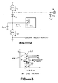
- this is achieved by the array shown schematically in FIG 2 which uses a pair of current sources I2, I1, connected to the sense amplifier with I2 being greater than I1.
- the difference between the two currents I2, I1, is the net current flow into the transistor Q1 of any selected cell.
- the full current I2 which can be significantly larger than the current I0 used in prior art bipolar memory arrays is available to discharge the bit line capacitance C BIT during bit line switching.
- a diode D12 is added in series with the smaller current source I1 between that current source and the node connected to the emitter 7 of the cell transistor.
- the diode D12 is necessary because current flow from current source I1 is desirable only on the column that is active.
- the diode D12 can be reverse biased by a COLUMN SELECT signal which reverse biases the diode of every column which is not selected during a given read operation.
- a diode D13 is added to limit the voltage swing of the sense nodes.
- the improvement achieved by this invention can be from 1 to 3 nanoseconds' reduction in switching time.
- the complete memory array of this invention is shown in FIG 4 and includes the bit lines B2, B4, a pair of which are connected to every cell in a column 22, and particularly the emitters 7, 8 of transistors Q1, Q2 of each column cell and the row select lines 24 one of which is connected to every cell in a row.
- One each of these row and bit lines are selectively activated to select a particular cell for reading at any given time.
- the capacitances C eb (the emitter base capacitance of the transistors) and C cs (the collector-substrate capacitance of the transistors) are also represented in this figure.
- the ability to use the large current I2 to charge and discharge these capacitances significantly speeds up the cell read times herein.
- the sense amplifier inputs 26 in this invention as can be clearly seen in FIG 4 are basically directly following the bit lines.
- the present system functions as a voltage follower to give an extremely rapid readout of the relative voltages on the two transistors in the cell. This provides extremely high speeds for reading the cells in the array.
- Other modifications of this invention may become apparent to a person of skill in the art who studies this invention disclosure. Therefore, the scope of this invention is to be limited only by the following claims.
Landscapes
- Engineering & Computer Science (AREA)
- Microelectronics & Electronic Packaging (AREA)
- Computer Hardware Design (AREA)
- Static Random-Access Memory (AREA)
- Semiconductor Memories (AREA)
Applications Claiming Priority (2)
| Application Number | Priority Date | Filing Date | Title |
|---|---|---|---|
| US33168489A | 1989-03-30 | 1989-03-30 | |
| US331684 | 1989-03-30 |
Publications (3)
| Publication Number | Publication Date |
|---|---|
| EP0390507A2 true EP0390507A2 (fr) | 1990-10-03 |
| EP0390507A3 EP0390507A3 (fr) | 1992-03-11 |
| EP0390507B1 EP0390507B1 (fr) | 1996-01-10 |
Family
ID=23294925
Family Applications (1)
| Application Number | Title | Priority Date | Filing Date |
|---|---|---|---|
| EP90303266A Expired - Lifetime EP0390507B1 (fr) | 1989-03-30 | 1990-03-27 | Circuit de décharge et de détection de ligne de bit |
Country Status (3)
| Country | Link |
|---|---|
| EP (1) | EP0390507B1 (fr) |
| JP (1) | JPH03116492A (fr) |
| DE (1) | DE69024689T2 (fr) |
Cited By (1)
| Publication number | Priority date | Publication date | Assignee | Title |
|---|---|---|---|---|
| CN113793815A (zh) * | 2021-09-26 | 2021-12-14 | 杭州广立微电子股份有限公司 | 一种宽电压范围高速多级放电电路、测试系统和放电方法 |
Families Citing this family (1)
| Publication number | Priority date | Publication date | Assignee | Title |
|---|---|---|---|---|
| CN101427320B (zh) * | 2006-04-24 | 2011-10-05 | Nxp股份有限公司 | 存储电路以及用于对存储元件进行读出的方法 |
Family Cites Families (2)
| Publication number | Priority date | Publication date | Assignee | Title |
|---|---|---|---|---|
| JPS5847792B2 (ja) * | 1979-07-26 | 1983-10-25 | 富士通株式会社 | ビット線制御回路 |
| EP0216264A1 (fr) * | 1985-09-19 | 1987-04-01 | Siemens Aktiengesellschaft | Dispositif de commande d'écriture et de lecture dans une mémoire ECL (à logique d'émetteur couplé) |
-
1990
- 1990-03-27 DE DE69024689T patent/DE69024689T2/de not_active Expired - Fee Related
- 1990-03-27 EP EP90303266A patent/EP0390507B1/fr not_active Expired - Lifetime
- 1990-03-30 JP JP2084774A patent/JPH03116492A/ja active Pending
Cited By (2)
| Publication number | Priority date | Publication date | Assignee | Title |
|---|---|---|---|---|
| CN113793815A (zh) * | 2021-09-26 | 2021-12-14 | 杭州广立微电子股份有限公司 | 一种宽电压范围高速多级放电电路、测试系统和放电方法 |
| CN113793815B (zh) * | 2021-09-26 | 2024-04-26 | 杭州广立测试设备有限公司 | 一种宽电压范围高速多级放电电路、测试系统和放电方法 |
Also Published As
| Publication number | Publication date |
|---|---|
| DE69024689T2 (de) | 1996-05-30 |
| EP0390507A3 (fr) | 1992-03-11 |
| DE69024689D1 (de) | 1996-02-22 |
| JPH03116492A (ja) | 1991-05-17 |
| EP0390507B1 (fr) | 1996-01-10 |
Similar Documents
| Publication | Publication Date | Title |
|---|---|---|
| US4924439A (en) | Semiconductor integrated circuit | |
| US4984207A (en) | Semiconductor memory device | |
| US4665505A (en) | Write circuit for use in semiconductor storage device | |
| EP0023792A2 (fr) | Mémoire à semi-conducteurs comprenant des cellules intégrées à injection logique | |
| EP0398048B1 (fr) | Dispositif de mémoire à semi-conducteur avec lecture de données à grande vitesse | |
| US4792923A (en) | Bipolar semiconductor memory device with double word lines structure | |
| US4369502A (en) | Semiconductor memory circuit | |
| US4459686A (en) | Semiconductor device | |
| EP0053504B1 (fr) | Mémoire statique semi-conductrice | |
| US5016214A (en) | Memory cell with separate read and write paths and clamping transistors | |
| US3688264A (en) | Operation of field-effect transistor circuits having substantial distributed capacitance | |
| US5200924A (en) | Bit line discharge and sense circuit | |
| US4651302A (en) | Read only memory including an isolation network connected between the array of memory cells and the output sense amplifier whereby reading speed is enhanced | |
| US4168539A (en) | Memory system with row clamping arrangement | |
| EP0503524B1 (fr) | Dispositif de mémoire à semi-conducteurs | |
| US4330853A (en) | Method of and circuit arrangement for reading and/or writing an integrated semiconductor storage with storage cells in MTL (I2 L) technology | |
| US4464735A (en) | Semiconductor memory | |
| EP0390507A2 (fr) | Circuit de décharge et de détection de ligne de bit | |
| US4520462A (en) | Semiconductor memory device | |
| JPS5948478B2 (ja) | 読出し専用メモリ | |
| US4070656A (en) | Read/write speed up circuit for integrated data memories | |
| US4456979A (en) | Static semiconductor memory device | |
| US4922411A (en) | Memory cell circuit with supplemental current | |
| EP0107912B1 (fr) | Dispositif de mémoire semi-conductrice | |
| US5117391A (en) | Bipolar memory cell array biasing technique with forward active PNP load cell |
Legal Events
| Date | Code | Title | Description |
|---|---|---|---|
| PUAI | Public reference made under article 153(3) epc to a published international application that has entered the european phase |
Free format text: ORIGINAL CODE: 0009012 |
|
| AK | Designated contracting states |
Kind code of ref document: A2 Designated state(s): DE FR GB NL |
|
| PUAL | Search report despatched |
Free format text: ORIGINAL CODE: 0009013 |
|
| AK | Designated contracting states |
Kind code of ref document: A3 Designated state(s): DE FR GB NL |
|
| 17P | Request for examination filed |
Effective date: 19920909 |
|
| 17Q | First examination report despatched |
Effective date: 19940202 |
|
| GRAA | (expected) grant |
Free format text: ORIGINAL CODE: 0009210 |
|
| AK | Designated contracting states |
Kind code of ref document: B1 Designated state(s): DE FR GB NL |
|
| PG25 | Lapsed in a contracting state [announced via postgrant information from national office to epo] |
Ref country code: NL Free format text: LAPSE BECAUSE OF FAILURE TO SUBMIT A TRANSLATION OF THE DESCRIPTION OR TO PAY THE FEE WITHIN THE PRESCRIBED TIME-LIMIT Effective date: 19960110 Ref country code: FR Effective date: 19960110 |
|
| REF | Corresponds to: |
Ref document number: 69024689 Country of ref document: DE Date of ref document: 19960222 |
|
| NLV1 | Nl: lapsed or annulled due to failure to fulfill the requirements of art. 29p and 29m of the patents act | ||
| EN | Fr: translation not filed | ||
| PLBE | No opposition filed within time limit |
Free format text: ORIGINAL CODE: 0009261 |
|
| STAA | Information on the status of an ep patent application or granted ep patent |
Free format text: STATUS: NO OPPOSITION FILED WITHIN TIME LIMIT |
|
| 26N | No opposition filed | ||
| REG | Reference to a national code |
Ref country code: GB Ref legal event code: IF02 |
|
| PGFP | Annual fee paid to national office [announced via postgrant information from national office to epo] |
Ref country code: DE Payment date: 20040819 Year of fee payment: 15 |
|
| PGFP | Annual fee paid to national office [announced via postgrant information from national office to epo] |
Ref country code: GB Payment date: 20050323 Year of fee payment: 16 |
|
| PG25 | Lapsed in a contracting state [announced via postgrant information from national office to epo] |
Ref country code: DE Free format text: LAPSE BECAUSE OF NON-PAYMENT OF DUE FEES Effective date: 20051001 |
|
| PG25 | Lapsed in a contracting state [announced via postgrant information from national office to epo] |
Ref country code: GB Free format text: LAPSE BECAUSE OF NON-PAYMENT OF DUE FEES Effective date: 20060327 |
|
| GBPC | Gb: european patent ceased through non-payment of renewal fee |
Effective date: 20060327 |