EP0390995A2 - Dispositif laser à semi-conducteur et méthode de sa production - Google Patents
Dispositif laser à semi-conducteur et méthode de sa production Download PDFInfo
- Publication number
- EP0390995A2 EP0390995A2 EP89307728A EP89307728A EP0390995A2 EP 0390995 A2 EP0390995 A2 EP 0390995A2 EP 89307728 A EP89307728 A EP 89307728A EP 89307728 A EP89307728 A EP 89307728A EP 0390995 A2 EP0390995 A2 EP 0390995A2
- Authority
- EP
- European Patent Office
- Prior art keywords
- current blocking
- blocking layer
- layer
- type
- conductivity
- Prior art date
- Legal status (The legal status is an assumption and is not a legal conclusion. Google has not performed a legal analysis and makes no representation as to the accuracy of the status listed.)
- Granted
Links
Images


Classifications
-
- H—ELECTRICITY
- H01—ELECTRIC ELEMENTS
- H01S—DEVICES USING THE PROCESS OF LIGHT AMPLIFICATION BY STIMULATED EMISSION OF RADIATION [LASER] TO AMPLIFY OR GENERATE LIGHT; DEVICES USING STIMULATED EMISSION OF ELECTROMAGNETIC RADIATION IN WAVE RANGES OTHER THAN OPTICAL
- H01S5/00—Semiconductor lasers
- H01S5/10—Construction or shape of the optical resonator, e.g. extended or external cavity, coupled cavities, bent-guide, varying width, thickness or composition of the active region
- H01S5/12—Construction or shape of the optical resonator, e.g. extended or external cavity, coupled cavities, bent-guide, varying width, thickness or composition of the active region the resonator having a periodic structure, e.g. in distributed feedback [DFB] lasers
-
- H—ELECTRICITY
- H01—ELECTRIC ELEMENTS
- H01S—DEVICES USING THE PROCESS OF LIGHT AMPLIFICATION BY STIMULATED EMISSION OF RADIATION [LASER] TO AMPLIFY OR GENERATE LIGHT; DEVICES USING STIMULATED EMISSION OF ELECTROMAGNETIC RADIATION IN WAVE RANGES OTHER THAN OPTICAL
- H01S5/00—Semiconductor lasers
- H01S5/20—Structure or shape of the semiconductor body to guide the optical wave ; Confining structures perpendicular to the optical axis, e.g. index or gain guiding, stripe geometry, broad area lasers, gain tailoring, transverse or lateral reflectors, special cladding structures, MQW barrier reflection layers
- H01S5/22—Structure or shape of the semiconductor body to guide the optical wave ; Confining structures perpendicular to the optical axis, e.g. index or gain guiding, stripe geometry, broad area lasers, gain tailoring, transverse or lateral reflectors, special cladding structures, MQW barrier reflection layers having a ridge or stripe structure
- H01S5/223—Buried stripe structure
- H01S5/2231—Buried stripe structure with inner confining structure only between the active layer and the upper electrode
-
- H—ELECTRICITY
- H01—ELECTRIC ELEMENTS
- H01S—DEVICES USING THE PROCESS OF LIGHT AMPLIFICATION BY STIMULATED EMISSION OF RADIATION [LASER] TO AMPLIFY OR GENERATE LIGHT; DEVICES USING STIMULATED EMISSION OF ELECTROMAGNETIC RADIATION IN WAVE RANGES OTHER THAN OPTICAL
- H01S5/00—Semiconductor lasers
- H01S5/10—Construction or shape of the optical resonator, e.g. extended or external cavity, coupled cavities, bent-guide, varying width, thickness or composition of the active region
- H01S5/12—Construction or shape of the optical resonator, e.g. extended or external cavity, coupled cavities, bent-guide, varying width, thickness or composition of the active region the resonator having a periodic structure, e.g. in distributed feedback [DFB] lasers
- H01S5/1231—Grating growth or overgrowth details
-
- H—ELECTRICITY
- H01—ELECTRIC ELEMENTS
- H01S—DEVICES USING THE PROCESS OF LIGHT AMPLIFICATION BY STIMULATED EMISSION OF RADIATION [LASER] TO AMPLIFY OR GENERATE LIGHT; DEVICES USING STIMULATED EMISSION OF ELECTROMAGNETIC RADIATION IN WAVE RANGES OTHER THAN OPTICAL
- H01S5/00—Semiconductor lasers
- H01S5/20—Structure or shape of the semiconductor body to guide the optical wave ; Confining structures perpendicular to the optical axis, e.g. index or gain guiding, stripe geometry, broad area lasers, gain tailoring, transverse or lateral reflectors, special cladding structures, MQW barrier reflection layers
- H01S5/22—Structure or shape of the semiconductor body to guide the optical wave ; Confining structures perpendicular to the optical axis, e.g. index or gain guiding, stripe geometry, broad area lasers, gain tailoring, transverse or lateral reflectors, special cladding structures, MQW barrier reflection layers having a ridge or stripe structure
- H01S5/2205—Structure or shape of the semiconductor body to guide the optical wave ; Confining structures perpendicular to the optical axis, e.g. index or gain guiding, stripe geometry, broad area lasers, gain tailoring, transverse or lateral reflectors, special cladding structures, MQW barrier reflection layers having a ridge or stripe structure comprising special burying or current confinement layers
- H01S5/2206—Structure or shape of the semiconductor body to guide the optical wave ; Confining structures perpendicular to the optical axis, e.g. index or gain guiding, stripe geometry, broad area lasers, gain tailoring, transverse or lateral reflectors, special cladding structures, MQW barrier reflection layers having a ridge or stripe structure comprising special burying or current confinement layers based on III-V materials
- H01S5/221—Structure or shape of the semiconductor body to guide the optical wave ; Confining structures perpendicular to the optical axis, e.g. index or gain guiding, stripe geometry, broad area lasers, gain tailoring, transverse or lateral reflectors, special cladding structures, MQW barrier reflection layers having a ridge or stripe structure comprising special burying or current confinement layers based on III-V materials containing aluminium
-
- H—ELECTRICITY
- H01—ELECTRIC ELEMENTS
- H01S—DEVICES USING THE PROCESS OF LIGHT AMPLIFICATION BY STIMULATED EMISSION OF RADIATION [LASER] TO AMPLIFY OR GENERATE LIGHT; DEVICES USING STIMULATED EMISSION OF ELECTROMAGNETIC RADIATION IN WAVE RANGES OTHER THAN OPTICAL
- H01S5/00—Semiconductor lasers
- H01S5/30—Structure or shape of the active region; Materials used for the active region
- H01S5/32—Structure or shape of the active region; Materials used for the active region comprising PN junctions, e.g. hetero- or double- heterostructures
- H01S5/323—Structure or shape of the active region; Materials used for the active region comprising PN junctions, e.g. hetero- or double- heterostructures in AIIIBV compounds, e.g. AlGaAs-laser, InP-based laser
- H01S5/32308—Structure or shape of the active region; Materials used for the active region comprising PN junctions, e.g. hetero- or double- heterostructures in AIIIBV compounds, e.g. AlGaAs-laser, InP-based laser emitting light at a wavelength less than 900 nm
-
- Y—GENERAL TAGGING OF NEW TECHNOLOGICAL DEVELOPMENTS; GENERAL TAGGING OF CROSS-SECTIONAL TECHNOLOGIES SPANNING OVER SEVERAL SECTIONS OF THE IPC; TECHNICAL SUBJECTS COVERED BY FORMER USPC CROSS-REFERENCE ART COLLECTIONS [XRACs] AND DIGESTS
- Y10—TECHNICAL SUBJECTS COVERED BY FORMER USPC
- Y10S—TECHNICAL SUBJECTS COVERED BY FORMER USPC CROSS-REFERENCE ART COLLECTIONS [XRACs] AND DIGESTS
- Y10S148/00—Metal treatment
- Y10S148/072—Heterojunctions
-
- Y—GENERAL TAGGING OF NEW TECHNOLOGICAL DEVELOPMENTS; GENERAL TAGGING OF CROSS-SECTIONAL TECHNOLOGIES SPANNING OVER SEVERAL SECTIONS OF THE IPC; TECHNICAL SUBJECTS COVERED BY FORMER USPC CROSS-REFERENCE ART COLLECTIONS [XRACs] AND DIGESTS
- Y10—TECHNICAL SUBJECTS COVERED BY FORMER USPC
- Y10S—TECHNICAL SUBJECTS COVERED BY FORMER USPC CROSS-REFERENCE ART COLLECTIONS [XRACs] AND DIGESTS
- Y10S148/00—Metal treatment
- Y10S148/095—Laser devices
Definitions
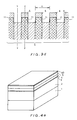
- the wafer having the groove 10 formed therein as shown in Figure 4d is placed in an apparatus for growing crystal by metalorganic thermal decomposition process.
- the wafer is heated, while hydrogen chloride is caused to flow over the wafer, so that the portion of the N-type GaAs first current blocking layer 5 exposed through the groove 10 is etched away and also portions of the first current blocking layer 5 are etched away with the strips of the grating-shaped second current blocking layer 6 acting as an etching mask, whereby the groove 10 in the first current blocking layer 5 changes in width between smaller and larger widths with the predetermined period ⁇ in the longitudinal direction of the groove 10.
Landscapes
- Physics & Mathematics (AREA)
- Condensed Matter Physics & Semiconductors (AREA)
- General Physics & Mathematics (AREA)
- Electromagnetism (AREA)
- Optics & Photonics (AREA)
- Geometry (AREA)
- Semiconductor Lasers (AREA)
- Physical Deposition Of Substances That Are Components Of Semiconductor Devices (AREA)
Applications Claiming Priority (2)
| Application Number | Priority Date | Filing Date | Title |
|---|---|---|---|
| JP88708/89 | 1989-04-06 | ||
| JP1088708A JPH0719931B2 (ja) | 1989-04-06 | 1989-04-06 | 半導体レーザ装置およびその製造方法 |
Publications (3)
| Publication Number | Publication Date |
|---|---|
| EP0390995A2 true EP0390995A2 (fr) | 1990-10-10 |
| EP0390995A3 EP0390995A3 (fr) | 1991-05-08 |
| EP0390995B1 EP0390995B1 (fr) | 1995-01-11 |
Family
ID=13950393
Family Applications (1)
| Application Number | Title | Priority Date | Filing Date |
|---|---|---|---|
| EP89307728A Expired - Lifetime EP0390995B1 (fr) | 1989-04-06 | 1989-07-28 | Dispositif laser à semi-conducteur et méthode de sa production |
Country Status (4)
| Country | Link |
|---|---|
| US (2) | US4984243A (fr) |
| EP (1) | EP0390995B1 (fr) |
| JP (1) | JPH0719931B2 (fr) |
| DE (1) | DE68920571T2 (fr) |
Cited By (2)
| Publication number | Priority date | Publication date | Assignee | Title |
|---|---|---|---|---|
| EP0905837A3 (fr) * | 1997-09-30 | 2000-09-27 | Mitsui Chemicals, Inc. | Dispositif laser à semiconducteur |
| EP1130723A3 (fr) * | 2000-03-01 | 2004-03-24 | Matsushita Electric Industrial Co., Ltd. | Dispositif laser à semiconducteur et méthode de fabrication |
Families Citing this family (20)
| Publication number | Priority date | Publication date | Assignee | Title |
|---|---|---|---|---|
| JPH088394B2 (ja) * | 1989-06-30 | 1996-01-29 | 三菱電機株式会社 | 半導体レーザおよびその製造方法 |
| JPH03293790A (ja) * | 1990-04-11 | 1991-12-25 | Eastman Kodak Japan Kk | 広ストライプ型レーザダイオード |
| US5268328A (en) * | 1990-09-07 | 1993-12-07 | Matsushita Electric Industrial Co., Ltd. | Method of fabricating a semiconductor laser |
| EP0475714B1 (fr) * | 1990-09-10 | 1995-12-27 | Sharp Kabushiki Kaisha | Dispositif laser à semi-conducteur à réaction distribuée et sa méthode de fabrication |
| JP2706369B2 (ja) * | 1990-11-26 | 1998-01-28 | シャープ株式会社 | 化合物半導体の成長方法及び半導体レーザの製造方法 |
| DE69220303T2 (de) * | 1991-07-24 | 1998-01-02 | Sharp Kk | Verfahren zur Herstellung eines Halbleiterlasers mit verteilter Rückkoppelung |
| US5346855A (en) * | 1993-01-19 | 1994-09-13 | At&T Bell Laboratories | Method of making an INP-based DFB laser |
| EP0627799B1 (fr) * | 1993-06-04 | 1997-10-08 | Sharp Kabushiki Kaisha | Dispositif semi-conducteur émettant de la lumière avec une troisième couche de gaine |
| US5398641A (en) * | 1993-07-27 | 1995-03-21 | Texas Instruments Incorporated | Method for p-type doping of semiconductor structures formed of group II and group VI elements |
| JPH07154024A (ja) * | 1993-11-30 | 1995-06-16 | Fuji Photo Film Co Ltd | 半導体レーザー |
| US6194240B1 (en) * | 1993-12-21 | 2001-02-27 | Lucent Technologies Inc. | Method for fabrication of wavelength selective electro-optic grating for DFB/DBR lasers |
| JPH07183618A (ja) * | 1993-12-22 | 1995-07-21 | Ricoh Co Ltd | 半導体レーザ装置、半導体レーザ装置製造方法並びに集積型半導体レーザ装置 |
| JPH0888439A (ja) * | 1994-09-16 | 1996-04-02 | Rohm Co Ltd | 半導体レーザおよびその製法 |
| JP4079393B2 (ja) * | 1998-03-10 | 2008-04-23 | シャープ株式会社 | 窒化物系化合物半導体レーザ素子及びその製造方法 |
| JP2000323789A (ja) * | 1999-05-11 | 2000-11-24 | Nec Corp | 窓型半導体レーザおよびその製造方法 |
| US6747259B1 (en) | 2000-10-03 | 2004-06-08 | Xerox Corporation | Assembly of imaging arrays for large format documents |
| JP2003133638A (ja) * | 2001-08-14 | 2003-05-09 | Furukawa Electric Co Ltd:The | 分布帰還型半導体レーザ素子及びレーザモジュール |
| US7369863B2 (en) * | 2001-11-30 | 2008-05-06 | Siemens Aktiengesellschaft | Positional data recording |
| JP2006190782A (ja) * | 2005-01-05 | 2006-07-20 | Fujitsu Ltd | 光半導体装置及びその製造方法 |
| JP2006202935A (ja) * | 2005-01-20 | 2006-08-03 | Nec Corp | 半導体レーザ及びその製造方法 |
Family Cites Families (12)
| Publication number | Priority date | Publication date | Assignee | Title |
|---|---|---|---|---|
| US4178604A (en) * | 1973-10-05 | 1979-12-11 | Hitachi, Ltd. | Semiconductor laser device |
| JPS59103393A (ja) * | 1982-12-06 | 1984-06-14 | Agency Of Ind Science & Technol | 半導体レ−ザの製造方法 |
| JPS59229889A (ja) * | 1983-06-13 | 1984-12-24 | Agency Of Ind Science & Technol | 半導体レ−ザ製造方法 |
| JPS6066484A (ja) * | 1983-09-22 | 1985-04-16 | Toshiba Corp | 半導体レ−ザ装置及びその製造方法 |
| JPS60192380A (ja) * | 1984-03-13 | 1985-09-30 | Mitsubishi Electric Corp | 半導体レ−ザ装置 |
| DE3437209A1 (de) * | 1984-10-10 | 1986-04-17 | Siemens AG, 1000 Berlin und 8000 München | Verbesserung zu einem monomoden-diodenlaser |
| US4837775A (en) * | 1985-10-21 | 1989-06-06 | General Electric Company | Electro-optic device having a laterally varying region |
| US4845014A (en) * | 1985-10-21 | 1989-07-04 | Rca Corporation | Method of forming a channel |
| JPS63140591A (ja) * | 1986-12-02 | 1988-06-13 | Mitsubishi Electric Corp | 半導体レ−ザ装置の製造方法 |
| JPS63166285A (ja) * | 1986-12-26 | 1988-07-09 | Toshiba Corp | 半導体発光装置の製造方法 |
| JP2768940B2 (ja) * | 1987-07-08 | 1998-06-25 | 三菱電機株式会社 | 単一波長発振半導体レーザ装置 |
| JPH073909B2 (ja) * | 1987-09-08 | 1995-01-18 | 三菱電機株式会社 | 半導体レーザの製造方法 |
-
1989
- 1989-04-06 JP JP1088708A patent/JPH0719931B2/ja not_active Expired - Lifetime
- 1989-07-28 DE DE68920571T patent/DE68920571T2/de not_active Expired - Fee Related
- 1989-07-28 EP EP89307728A patent/EP0390995B1/fr not_active Expired - Lifetime
- 1989-08-01 US US07/387,767 patent/US4984243A/en not_active Expired - Fee Related
-
1990
- 1990-10-10 US US07/597,782 patent/US5079185A/en not_active Expired - Fee Related
Cited By (4)
| Publication number | Priority date | Publication date | Assignee | Title |
|---|---|---|---|---|
| EP0905837A3 (fr) * | 1997-09-30 | 2000-09-27 | Mitsui Chemicals, Inc. | Dispositif laser à semiconducteur |
| US6285699B1 (en) | 1997-09-30 | 2001-09-04 | Mitsui Chemicals Inc. | Semiconductor laser device |
| EP1130723A3 (fr) * | 2000-03-01 | 2004-03-24 | Matsushita Electric Industrial Co., Ltd. | Dispositif laser à semiconducteur et méthode de fabrication |
| US7050472B2 (en) | 2000-03-01 | 2006-05-23 | Matsushita Electric Industrial Co., Ltd. | Semiconductor laser device and method for manufacturing the same |
Also Published As
| Publication number | Publication date |
|---|---|
| US4984243A (en) | 1991-01-08 |
| DE68920571D1 (de) | 1995-02-23 |
| JPH0719931B2 (ja) | 1995-03-06 |
| US5079185A (en) | 1992-01-07 |
| EP0390995B1 (fr) | 1995-01-11 |
| DE68920571T2 (de) | 1995-05-18 |
| EP0390995A3 (fr) | 1991-05-08 |
| JPH02266583A (ja) | 1990-10-31 |
Similar Documents
| Publication | Publication Date | Title |
|---|---|---|
| EP0390995B1 (fr) | Dispositif laser à semi-conducteur et méthode de sa production | |
| US5872022A (en) | Method for etching a semiconductor method for fabricating semiconductor device method for fabricating semiconductor laser and semiconductor laser | |
| JP2823476B2 (ja) | 半導体レーザおよびその製造方法 | |
| EP1437809B1 (fr) | Laser à semi-conducteur composé | |
| US5518955A (en) | Method of fabricating quantum wire | |
| US5966396A (en) | Gallium nitride-based compound semiconductor laser and method of manufacturing the same | |
| JPH0758823B2 (ja) | 幾何学的ドーピング法および同法により製造の電子デバイス | |
| JPH04216693A (ja) | 自己安定化半導体回折格子の製作方法 | |
| US4149175A (en) | Solidstate light-emitting device | |
| EP1265326A1 (fr) | Dispositif laser a semi-conducteur a retroaction repartie et a couplage de gain et son procede de production | |
| EP0264225B1 (fr) | Dispositif laser à semi-conducteur et sa méthode de fabrication | |
| US5546418A (en) | Semiconductor laser having a flat groove for selected crystal planes | |
| JPH06252510A (ja) | 利得結合分布帰還型半導体レーザとその作製方法 | |
| EP0602579A1 (fr) | Laser à semi-conducteur et méthode de fabrication | |
| EP0321294B1 (fr) | Dispositif laser à semi-conducteur | |
| US5588016A (en) | Semiconductor laser device | |
| KR0153585B1 (ko) | 메사 스트라이프 구조를 가진 반도체 레이저 및 그의 제조방법 | |
| JP2686306B2 (ja) | 半導体レーザ装置とその製造方法 | |
| EP0915542B1 (fr) | Laser à semiconducteur avec des couches de blocage du courant améliorées et méthode de fabrication | |
| US5157681A (en) | Wavelength-tunable distributed Bragg reflector semiconductor laser | |
| US5518954A (en) | Method for fabricating a semiconductor laser | |
| EP1233492B1 (fr) | Procédé de fabrication pour laser sémi-conducteur composé | |
| US4432092A (en) | Semiconductor laser | |
| JP3139886B2 (ja) | 半導体レーザ素子およびその製造方法 | |
| JPH0923039A (ja) | 半導体レーザの製造方法 |
Legal Events
| Date | Code | Title | Description |
|---|---|---|---|
| PUAI | Public reference made under article 153(3) epc to a published international application that has entered the european phase |
Free format text: ORIGINAL CODE: 0009012 |
|
| AK | Designated contracting states |
Kind code of ref document: A2 Designated state(s): DE FR GB NL |
|
| 17P | Request for examination filed |
Effective date: 19901207 |
|
| PUAL | Search report despatched |
Free format text: ORIGINAL CODE: 0009013 |
|
| AK | Designated contracting states |
Kind code of ref document: A3 Designated state(s): DE FR GB NL |
|
| 17Q | First examination report despatched |
Effective date: 19920924 |
|
| GRAA | (expected) grant |
Free format text: ORIGINAL CODE: 0009210 |
|
| AK | Designated contracting states |
Kind code of ref document: B1 Designated state(s): DE FR GB NL |
|
| REF | Corresponds to: |
Ref document number: 68920571 Country of ref document: DE Date of ref document: 19950223 |
|
| ET | Fr: translation filed | ||
| PLBE | No opposition filed within time limit |
Free format text: ORIGINAL CODE: 0009261 |
|
| STAA | Information on the status of an ep patent application or granted ep patent |
Free format text: STATUS: NO OPPOSITION FILED WITHIN TIME LIMIT |
|
| 26N | No opposition filed | ||
| REG | Reference to a national code |
Ref country code: GB Ref legal event code: 746 Effective date: 19960611 |
|
| REG | Reference to a national code |
Ref country code: FR Ref legal event code: D6 |
|
| PGFP | Annual fee paid to national office [announced via postgrant information from national office to epo] |
Ref country code: FR Payment date: 20000711 Year of fee payment: 12 |
|
| PGFP | Annual fee paid to national office [announced via postgrant information from national office to epo] |
Ref country code: DE Payment date: 20000724 Year of fee payment: 12 |
|
| PGFP | Annual fee paid to national office [announced via postgrant information from national office to epo] |
Ref country code: GB Payment date: 20000726 Year of fee payment: 12 |
|
| PGFP | Annual fee paid to national office [announced via postgrant information from national office to epo] |
Ref country code: NL Payment date: 20000728 Year of fee payment: 12 |
|
| PG25 | Lapsed in a contracting state [announced via postgrant information from national office to epo] |
Ref country code: GB Free format text: LAPSE BECAUSE OF NON-PAYMENT OF DUE FEES Effective date: 20010728 |
|
| PG25 | Lapsed in a contracting state [announced via postgrant information from national office to epo] |
Ref country code: NL Free format text: LAPSE BECAUSE OF NON-PAYMENT OF DUE FEES Effective date: 20020201 |
|
| GBPC | Gb: european patent ceased through non-payment of renewal fee |
Effective date: 20010728 |
|
| PG25 | Lapsed in a contracting state [announced via postgrant information from national office to epo] |
Ref country code: FR Free format text: LAPSE BECAUSE OF NON-PAYMENT OF DUE FEES Effective date: 20020329 |
|
| NLV4 | Nl: lapsed or anulled due to non-payment of the annual fee |
Effective date: 20020201 |
|
| PG25 | Lapsed in a contracting state [announced via postgrant information from national office to epo] |
Ref country code: DE Free format text: LAPSE BECAUSE OF NON-PAYMENT OF DUE FEES Effective date: 20020501 |
|
| REG | Reference to a national code |
Ref country code: FR Ref legal event code: ST |