EP0393602A2 - Driver pour imprimante à jet d'encre - Google Patents
Driver pour imprimante à jet d'encre Download PDFInfo
- Publication number
- EP0393602A2 EP0393602A2 EP90107288A EP90107288A EP0393602A2 EP 0393602 A2 EP0393602 A2 EP 0393602A2 EP 90107288 A EP90107288 A EP 90107288A EP 90107288 A EP90107288 A EP 90107288A EP 0393602 A2 EP0393602 A2 EP 0393602A2
- Authority
- EP
- European Patent Office
- Prior art keywords
- ink
- scanning voltage
- generating means
- driver
- time constant
- Prior art date
- Legal status (The legal status is an assumption and is not a legal conclusion. Google has not performed a legal analysis and makes no representation as to the accuracy of the status listed.)
- Granted
Links
Images


Classifications
-
- B—PERFORMING OPERATIONS; TRANSPORTING
- B41—PRINTING; LINING MACHINES; TYPEWRITERS; STAMPS
- B41J—TYPEWRITERS; SELECTIVE PRINTING MECHANISMS, i.e. MECHANISMS PRINTING OTHERWISE THAN FROM A FORME; CORRECTION OF TYPOGRAPHICAL ERRORS
- B41J2/00—Typewriters or selective printing mechanisms characterised by the printing or marking process for which they are designed
- B41J2/005—Typewriters or selective printing mechanisms characterised by the printing or marking process for which they are designed characterised by bringing liquid or particles selectively into contact with a printing material
- B41J2/01—Ink jet
- B41J2/015—Ink jet characterised by the jet generation process
- B41J2/04—Ink jet characterised by the jet generation process generating single droplets or particles on demand
- B41J2/045—Ink jet characterised by the jet generation process generating single droplets or particles on demand by pressure, e.g. electromechanical transducers
- B41J2/04501—Control methods or devices therefor, e.g. driver circuits, control circuits
- B41J2/0452—Control methods or devices therefor, e.g. driver circuits, control circuits reducing demand in current or voltage
-
- B—PERFORMING OPERATIONS; TRANSPORTING
- B41—PRINTING; LINING MACHINES; TYPEWRITERS; STAMPS
- B41J—TYPEWRITERS; SELECTIVE PRINTING MECHANISMS, i.e. MECHANISMS PRINTING OTHERWISE THAN FROM A FORME; CORRECTION OF TYPOGRAPHICAL ERRORS
- B41J2/00—Typewriters or selective printing mechanisms characterised by the printing or marking process for which they are designed
- B41J2/005—Typewriters or selective printing mechanisms characterised by the printing or marking process for which they are designed characterised by bringing liquid or particles selectively into contact with a printing material
- B41J2/01—Ink jet
- B41J2/015—Ink jet characterised by the jet generation process
- B41J2/04—Ink jet characterised by the jet generation process generating single droplets or particles on demand
- B41J2/045—Ink jet characterised by the jet generation process generating single droplets or particles on demand by pressure, e.g. electromechanical transducers
- B41J2/04501—Control methods or devices therefor, e.g. driver circuits, control circuits
- B41J2/04541—Specific driving circuit
-
- B—PERFORMING OPERATIONS; TRANSPORTING
- B41—PRINTING; LINING MACHINES; TYPEWRITERS; STAMPS
- B41J—TYPEWRITERS; SELECTIVE PRINTING MECHANISMS, i.e. MECHANISMS PRINTING OTHERWISE THAN FROM A FORME; CORRECTION OF TYPOGRAPHICAL ERRORS
- B41J2/00—Typewriters or selective printing mechanisms characterised by the printing or marking process for which they are designed
- B41J2/005—Typewriters or selective printing mechanisms characterised by the printing or marking process for which they are designed characterised by bringing liquid or particles selectively into contact with a printing material
- B41J2/01—Ink jet
- B41J2/015—Ink jet characterised by the jet generation process
- B41J2/04—Ink jet characterised by the jet generation process generating single droplets or particles on demand
- B41J2/045—Ink jet characterised by the jet generation process generating single droplets or particles on demand by pressure, e.g. electromechanical transducers
- B41J2/04501—Control methods or devices therefor, e.g. driver circuits, control circuits
- B41J2/04581—Control methods or devices therefor, e.g. driver circuits, control circuits controlling heads based on piezoelectric elements
-
- B—PERFORMING OPERATIONS; TRANSPORTING
- B41—PRINTING; LINING MACHINES; TYPEWRITERS; STAMPS
- B41J—TYPEWRITERS; SELECTIVE PRINTING MECHANISMS, i.e. MECHANISMS PRINTING OTHERWISE THAN FROM A FORME; CORRECTION OF TYPOGRAPHICAL ERRORS
- B41J2/00—Typewriters or selective printing mechanisms characterised by the printing or marking process for which they are designed
- B41J2/005—Typewriters or selective printing mechanisms characterised by the printing or marking process for which they are designed characterised by bringing liquid or particles selectively into contact with a printing material
- B41J2/01—Ink jet
- B41J2/015—Ink jet characterised by the jet generation process
- B41J2/04—Ink jet characterised by the jet generation process generating single droplets or particles on demand
- B41J2/045—Ink jet characterised by the jet generation process generating single droplets or particles on demand by pressure, e.g. electromechanical transducers
- B41J2/04501—Control methods or devices therefor, e.g. driver circuits, control circuits
- B41J2/04588—Control methods or devices therefor, e.g. driver circuits, control circuits using a specific waveform
Definitions
- the present invention relates to an ink-jet printer driver in which electrostriction elements are caused to press ink to jet ink out of nozzles so as to form characters/graphics with ink dot matrices.
- reference numeral 1 designates a nozzle plate having a nozzle 1a
- 2 designates an elastic plate
- 3 designates liquid ink
- 4 designates an electrostriction element which is distorted by an electric field. The electrostriction element is closely attached on the elastic plate 2.
- Fig. 11(a) shows a standby condition in which the elastic plate 2 is projected toward ink by the distortion of the electrostriction element 4.
- Figs. 11(b) through 11(d) show the steps in which the elastic plate 2 is recovered to its neutral point by gradually removing the electric field from the electrostriction element 4, respectively.
- Fig. 11(e) shows a condition in which an electric field is suddenly applied to the electrostriction element 4 to make the elastic plate 2 project toward the ink 3 to thereby jet the ink 3 outward. If the application of the electric field is continued as it is, the head returns to its standby condition, as shown in Fig. 11(a).
- the electrostriction element 4 is provided within ink.
- the present invention is applied to both the methods.
- a printer head is constituted by combining a plurality of aforementioned constructions.
- the number of the constructions is from 8 to 64.
- the number of the constructions is from 1400 to 4000.
- FIG. 12 A conventional art for driving the aforementioned printer head is shown in Figs. 12 and 13.
- reference numeral 5 designates a high-voltage electric source which, in general, has an output voltage V0 within a range of from 50 to 200V. The output voltage may vary in accordance with the characteristics of constituent parts due to the response frequency.
- Symbol TR S represents a P-type transistor for switching a voltage V0 so as to feed a signal V X to the printer head.
- Reference numeral 6 i designates one driving circuit.
- an electrostriction element 7 i is charged to a voltage V0 through a resistor R having a value of several M ⁇ , so that the situation is returned to the aforementioned standby state.
- a diode D i for isolating the driving circuit from other driving circuits and a resistor R li serve to charge the electrostriction element 7 i rapdily.
- an N-type transistor TR Di is turned on, the charge of the electrostriction element 7 i is absorbed through a resistor R21, having a larger resistance value than that of the resistor R 1i , so that the voltage drops as shown in the point A in Fig. (13(b).
- the symbol i attached to the driving circuit 6 i , the electrostriction element 7 i , and other parts in the driving circuit 6 i is used to show those parts or components representatively because a plurality of such driving circuits are provided respectively for a plurality of printer heads as described above.
- Reference numeral 8 designates a driving signal generating means which serves to give a switching signal to the transistor TR S periodically.
- a driving signal is given to the transistor TR Di in accordance with existence of a dot forming instruction.
- Fig. (13(a) shows a state of the transistor TR S for performing a switching operation periodically.
- the electrostriction element 7 i In the case where the charge of the electrostriction element 7 i has been absorbed, the electrostriction element 7 i is charged rapidly through the diode D i and the resistor R 1i during in the ON-state of the transistor TR S so that ink is jetted as shown in Fig. 11(e). On the contrary, in the case where the electrostriction element 7 i has been charged to a value of V0, the charged voltage of the electrostriction element 7 i does not change so that ink is not jetted.
- the resistance value of the resistor R 1i is selected to be several k ⁇ and the charging time constant is selected to be a value in a range of from 5 to 10 ⁇ s so as to prevent occurrence of wasteful ink jetting caused by overshooting of the elastic plate 2.
- the resistance value of the resistor R 2i is selected to be of the order of several tens of k ⁇ and the charging time constant is selected to be a value within a range of from 20 to 100 ⁇ s so as to prevent occurrence of both wasteful ink jetting caused by an undercoat and air suction from nozzles. If air is sucked into ink, it becomes impossible to perform ink jetting only by contraction of air.
- the equivalent capacitance of the electrostriction element 7 i is within a range of from 100 to 1000 PF.
- the foregoing is that related to a conventional ink-jet printer driver.
- the present invention is directed to solve the above problems in the prior art, and an object thereof is to provide an ink-jet printer driver in which charge absorbing/injecting characteristics of electrostriction elements used as main constituent parts of a printer can be set freely.
- the present invention has the following features:
- the ink-jet printer driver comprises: a scanning voltage generating means for generating a scanning voltage having a predetermined waveform; a plurality of gating means for respectively giving the scanning voltage to the electrostriction elements corresponding to the gating means; and a driving signal generating means for giving driving signals to the plurality of gating means respectively.
- a scanning voltage generating means for generating a scanning voltage having a predetermined waveform
- a plurality of gating means for respectively giving the scanning voltage to the electrostriction elements corresponding to the gating means
- a driving signal generating means for giving driving signals to the plurality of gating means respectively.
- the scanning voltage generating means is composed of first and second switching means for defining the rising and falling of the scanning voltage, and a feedback circuit including coil means.
- the scanning voltage generating means is composed of a time constant circuit constituted by a resistor and a capacitor, a switching means for actuating the time constant circuit to operate in a predetermined cycle, and an amplifier for putting out the voltage change caused in the time constant circuit as a low- impedance output signal.
- the voltage change is not affected by the load containing the electrostriction elements.
- the ink-jet printer is a serial printer having a carriage of the type designed to move a printer head constituted by the nozzles and the electrostriction elements
- the gating means and the driving signal generating means are mounted on the carriage to simplify a connection cable between the carriage and a fixed control portion of the printer.
- the number of electric source lines and the number of signal lines can be reduced and, accordingly, a connection cable between the carriage and a fixed control portion of the printer can be simplified to reduce cost.
- time constants are set respectively in the individual drive elements.
- the scanning voltage having a predetermined waveform is selected so that the driving elements can be simplified to facilitate integration of the circuits.
- the driving elements are prepared in the form of ICs, the driving elements can be mounted on the printer head easily, so that cost on the whole of the printer can be saved.
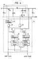
- Fig. 1 there is shown an embodiment of the present invention.
- the symbol C0 represents a smoothing capacitor included in a high-voltage electric source 5
- the symbol C1 represents a capacitor inclusive of capacitance of electrostriction elements and additive capacitance.
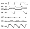
- the reference numeral 10 designated a scanning voltage generating means in which the output voltage changes within a range between V0 and GND as shown in the waveform Fig. 2(a).
- the refrence numeral 11 designates a driver portion composed of a plurality of gating means 12 and a plurality of electrostriction elements 13.
- Each gating means 12 selects a scanning voltage V S of the scanning voltage generating means 10 based on a driving signal to feed the scanning voltage to a corresponding electrostriction element 13.
- the reference numeral 15 designates a driving signal generating means for feeding a driving signal to a control terminal of each gating means 12.
- the driving signal generating means 15 has a shift register 19 for storing data while successively shifting the data based on a shift clock signal, a latch circuit 20 for simultaneously latching the data stored by the shift register 19 based on a latch pulse signal, an enable circuit 21 for releasing the data latched by the latch circuit 20 based on an enable signal, two- input OR gates 17 for receiving both the data put out from the enable circuit 21 and the latch pulse signal, and a level changer 16 for changing the levels of the output signals of the OR gates 17 to feed control signals to the gating means 12.
- the level changer 16 serves to change the respective levels of the output signals of the OR gages 17 into V0 to make the corresponding gating means operate. This is because the parts other than the driving signal generating means are operated at 5V and therefore it is impossible to make the gating operate if the level of the output signal of each OR gate 17 is converted into V0.
- the latch pulse signal is fed to the OR gate 17 so that the gating means 12 is opened to compensate leakage of the electrostriction element 13 while the scanning voltage V S takes the value of V0. In short, this serves for the resistor R Si in Fig. 12.
- Fig. 2(b) shows the latch pulse signal.
- Fig. 2(c) shows an example of the selection signal issued by the enable circuit 21 to jet ink.
- Fig. 2(c) shows an example of the waveform of the driving signal applied to the electrostriction element 13.
- ink is jetted out of nozzles corresponding to the electrostriction elements with their charged voltages lowered in the same manner as in Fig. 13(b).
- the reference numeral 14 designates a scanning control means for feeding an operation timing signal to the scanning voltage generating means 10 after changing the level thereof by a level changer 14a based on both the shift clock signal and the latch pulse signal.
- symbols TR1 represents a P-type transistor which is supplied with an ON-OFF switching signal as shown in Fig. 3(a) by the scanning control means 14.
- the scanning control means 14 When the transistor TR1 is turned on, the voltage V0 is switched by the transistor TR1 to charge the capacitor C1 through a coil L1.
- the scanning voltage V S is fed back to the scanning control means 14 through a line 25 to thereby control the ON-OFF switching signal in a manner as shown in Fig. 3(a).
- the transistor TR1 When the transistor TR1 is in the OFF state, a current flowing in the coil L1 is passed through a diode PD to charge the capacitor C1 further. When the charged voltage of the capacitor C1 approached V0 according to the predetermined rising characteristic thereof, the transistor TR1 is kept as it is in the OFF state.
- the coil L1 serves to charge the capacitor C1 through the diode PD in the form of electromagnetic energy after the turn off of the transistor TR1 to thereby prevent energy of the high- voltage electric source from being consumed by 50 % or more by the resistors in the system.
- the scanning control means 14 feeds an ON-OFF switching signal as shown in Fig. 3(b) to an N-type transistor TR2.
- the energy for charging the capacitor C1 is converted into electromagnetic energy of a coil L2 and then the electromagnetic energy is transferred to a capacitor C0 through a diode RD after turning off of the transistor TR2.
- the capacitance value of the capacitor C1 changes because it includes capacitance of selected electrostriction elements 13.
- the scanning control means 14 adjusts energy transfer speed by controlling the number of times of switching of the transistor TR2 while detecting the charged voltage of the capacitor C1 to thereby attain the predetermined rising characteristic of the scanning voltage V S .
- the scanning voltage generating means 10 in Fig. 4 serves to generate a predetermined scanning voltage V S and perform energy exchange between the high-voltage electric source 5 and the capacitor C1. Accordingly, wasteful power consumption can be saved.
- the reference numerals 26 and 27 designate first and second counters for counting the number of shift clock pulses.
- Each of the first and second counters 26 and 27 has a preset terminal for presetting both a start point of time and an operation time width in accordance with the latch pulse signal.
- the reference numerals 28 and 29 designate digital-to-analog converters (hereinafter referred to as "D/A converters") for converting the contents of the first and second counters in the form of digital signals into analog signals, respectively.
- D/A converters digital-to-analog converters
- the reference numerals 32 and 31 designate comparators with their one inputs supplied with the shift scanning voltage V S commonly to each other and their other inputs supplied with the output output signals of the D/A converters 28 and 29 respectively.
- the comparators 30 and 31 output their output signals when the level of the scanning voltage V S is low and when it is high, respectively.
- the reference numerals 32 and 33 designate AND gates with their one inputs supplied with the shift clock commonly to each other and their other inputs supplied with the output signals of the comparators 30 and 31 respectively.
- the frequency of the shift clock signal is set to a value in a range of from 100 kHz to several MHz.
- the output signals of the AND gates 32 and 33 are respectively connected to the control electrodes of the transistors TR1 and TR2 after level-converted through a level changer 34 and directly, respectively.
- the target scanning voltage and the result scanning voltage V S in the thus configured voltage generating means 10 and the scanning control means 14 have waveforms shown in the solid line and the broken line in Fig. 3(c), respectively.
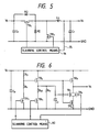
- the coils L1 and L2 of Fig. 4 are replaced by a single coil L3 in Fig. 5.
- the two coils L1 and L2 are used to facilitate control because the rising of the scanning voltage V S and the falling thereof are different from each other.
- the scanning voltage V S is generated by a time constant circuit composed of a capacitor and a resistor, without feedback control.
- a different reference numeral 40 is therefore given to the scanning control means.
- Resistors R3 and R4 and an N-type transistor TR3 serve as a level changer to generate a signal as shown in Fig. 7(a) to turn-on P-type transistors TR4 and TR6 simultaneously with each other.
- the turning-on of the transistor TR6 gives the rising characteristic of a scanning voltage V S as shown in Fig. 7(d).
- the turning-on of the transistor TR4 serves to charge a time-constant capacitor C T into the voltage V0 rapidly.
- an N-type transistor TR8 is turned on to activate a P-type transistor TR7 as a source follower to thereby change the charged voltage of the time-constant capacitor C T into low impedance, so that the scanning voltage V S having a falling characteristic as shown in Fig. 7(d) is put out.
- the time constant in the falling of the scanning voltage V S determined by the time-constant capacitor C T and the time-constant resistors R 1T and R 2T .
- the resistor R 2T When the N-type transistor TR5 is turned on in the timing as shown in Fig. 7(c), the resistor R 2T operates to shorten the time constant. The falling characteristic is shown in the solid line in Fig. 7(d). The broken line in Fig. 7(d) shows the case where the value of the resistor R 1T is reduced to a small resistance value.
- a desired rising characteristic can be attained by addition of the same combination as the combination of the transistor TR5 and the resistor R 2T .
- the N-type transistor TR9 is turned on as shown in Fig. 7(b) to change the level of the scanning voltage V S forcedly into the GND level.
- the transistor TR9 is provided for the purpose of facilitating the operation of the transistor TR7, because the transistor TR7 as a source follower cannot operate when the gate voltage reaches a cut-off voltage, and because a considerably large time is required for changing the charged voltage of the capacitor C T into the GND level.
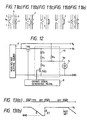
- Fig. 8 shows the case where not only the scanning voltage is generated based on a time constant formed by a capacitor and a resistor but the rising characteristic is determined based on the time constant. In Fig. 8, the scanning control means is not shown.
- the capacitor C T is charged through the resistor R 3T .
- the charged voltage of the capacitor C T is put out as the scanning voltage V S through low impedance of the N-type transistor TR11 in a source follower connection. This is the rising portion of the scanning voltage shown in Fig. 9(d).
- the P-type transistor TR12 serves to change the scanning voltage into a final voltage V0.
- the transistor TR8 is turned on to activate the transistor TR7 to thereby output the scanning voltage V S having rising characteristic formed in the same manner as in Fig. 6.
- the falling of the scanning voltage is carried out by discharging the capacitor C T through the resistor R 4T disposed between the capacitor C T and the transistor TR13.
- Figs. 9(b) and 9(c) show the timing of the turning-on of the transistor TR12 and the timing of the turning-on of the transistor TR9, respectively.
- a desired program can be attained by changing the time constant of the time-constant circuit or by addition of resistors and switching circuits.
- the reference numeral 50 designates a level changer constituted by a bistable or flip-flop circuit composed of P-type transistors TR14 and TR15 and N-type transistors TR16 and TR17.
- the flip-flop circuit has an advantage in that power is consumed only when the state thereof is changed.
- the reference numeral 53 designates a signal of a level of about 5V. The level of this signal is changed into the level of V0 by the level changer 50.
- An N-type transistor TR18 is turned on in the presence of the signal.
- an N-type transistor TR19 is turned off because the signal is inverted by an inverter 52.
- electric power is consumed by the resistors R3 and R4 when the transistor TR3 is in the ON state.
- transistor TR8 in Fig. 6 and the transistors TR6 and TR8 in Fig. 8 have a purpose of preventing damage of transistors caused by short-circuit of the electric source.
- the level changer in Fig. 10 is constituted by a bistable or flip-flop circuit composed of four transistors. Accordingly, at least one of the transistors is in the OFF state against the electric source. Accordingly, current flowing occurs only in a transition period, so that power consumption is extremely small.
- N-type transistors TR20 and a P-type transistor TR21 in the gating means 51 are made conductive simultaneously with each other.
- the gating means 51 carries out a two-way gating operation, so that the gating means 51 is used in common to two input/output devices IO1 and IO2 as shown by the two-head arrows.
- the gating means and the driving signal generating means can be constituted by transistors without using any other parts. Accordingly, the means can be prepared easily in the form of ICs.
- the printer can be simplified in construction so that cost can be saved.
- connection lines equal in number to the nozzles and two or four connection cables to the fixed portion are required.
- this invention only one connection cable is required and the number of connection lines can be reduced.
- the total number of lines is eight, namely, two lines for the scanning voltage V S , two electric source lines for the driving signal generating means, and four lines for the shift clock signal, the data signal, the latch pulse signal and the enable signal. Accordingly, cost can be saved.
- the space factor in the fixed portion of the printer is improved to attain reduction both in size as well as in cost.
- the scanning voltage is fed back to predetermined means and parts after conversion thereof into electromagnetic energy, heat genera tion and cost can be reduced when the scanning voltage is generated.
- the portion including the driving signal generating means and the grating means can be constituted by pairs of P-type and N-type transistors. In this case, not only power consumption can be saved but these means can be prepared in the form of ICs. Accordingly, the present invention can make a large contribution to reliability and cost saving.
Landscapes
- Particle Formation And Scattering Control In Inkjet Printers (AREA)
- Ink Jet (AREA)
Applications Claiming Priority (6)
| Application Number | Priority Date | Filing Date | Title |
|---|---|---|---|
| JP97162/89 | 1989-04-17 | ||
| JP9716289A JP2814539B2 (ja) | 1989-04-17 | 1989-04-17 | インク噴射プリンタの駆動装置 |
| JP17143089A JPH0336036A (ja) | 1989-07-03 | 1989-07-03 | インク噴射プリンタの制御装置 |
| JP171430/89 | 1989-07-03 | ||
| JP273051/89 | 1989-10-20 | ||
| JP27305189A JPH03133647A (ja) | 1989-10-20 | 1989-10-20 | インク噴射プリンタの駆動装置 |
Publications (3)
| Publication Number | Publication Date |
|---|---|
| EP0393602A2 true EP0393602A2 (fr) | 1990-10-24 |
| EP0393602A3 EP0393602A3 (fr) | 1991-11-21 |
| EP0393602B1 EP0393602B1 (fr) | 1995-03-22 |
Family
ID=27308340
Family Applications (1)
| Application Number | Title | Priority Date | Filing Date |
|---|---|---|---|
| EP90107288A Expired - Lifetime EP0393602B1 (fr) | 1989-04-17 | 1990-04-17 | Driver pour imprimante à jet d'encre |
Country Status (4)
| Country | Link |
|---|---|
| US (1) | US5347300A (fr) |
| EP (1) | EP0393602B1 (fr) |
| DE (1) | DE69017936T2 (fr) |
| HK (1) | HK94097A (fr) |
Cited By (7)
| Publication number | Priority date | Publication date | Assignee | Title |
|---|---|---|---|---|
| EP0548984A1 (fr) * | 1991-12-26 | 1993-06-30 | Seiko Epson Corporation | Circuit de commande pour tête d'impression à jet d'encre |
| EP0568902A3 (fr) * | 1992-05-02 | 1994-03-02 | Westonbridge Int Ltd | |
| EP0626266A3 (fr) * | 1993-05-27 | 1995-11-22 | Canon Kk | Appareil d'enregistrement commandé par les caractéristiques de la tête et méthode d'enregistrement. |
| EP0646461A3 (fr) * | 1993-10-05 | 1997-11-05 | Seiko Epson Corporation | Méthode et appareil pour commander une tête d'enregistrement à jet d'encre |
| EP1078748A3 (fr) * | 1999-08-20 | 2001-05-16 | Ngk Insulators, Ltd. | Circuit de commande d'un appareil à éjection de gouttes de liquide |
| US6243111B1 (en) | 1993-09-02 | 2001-06-05 | Canon Kabushiki Kaisha | Print head substrate, print head using the same, and printing apparatus |
| USRE44825E1 (en) | 1993-09-03 | 2014-04-08 | Canon Kabushiki Kaisha | Print head substrate, print head using the same, and printing apparatus |
Families Citing this family (4)
| Publication number | Priority date | Publication date | Assignee | Title |
|---|---|---|---|---|
| JPH1086450A (ja) * | 1996-07-23 | 1998-04-07 | Canon Inc | プリント装置およびプリント方法 |
| JP3731346B2 (ja) * | 1998-05-19 | 2006-01-05 | ブラザー工業株式会社 | アクチュエータの駆動回路 |
| US5936371A (en) * | 1999-02-16 | 1999-08-10 | Lexmark International, Inc. | Method and apparatus for controlling a servo motor using a stepper motor controller integrated circuit |
| CA2311104C (fr) * | 1999-06-04 | 2004-07-13 | Canon Kabushiki Kaisha | Tete d'ecriture a jet d'encre, et dispositif d'ecriture a jet d'encre |
Family Cites Families (10)
| Publication number | Priority date | Publication date | Assignee | Title |
|---|---|---|---|---|
| US4240081A (en) * | 1978-10-13 | 1980-12-16 | Dennison Manufacturing Company | Ink jet printing |
| JPS5660261A (en) * | 1979-10-23 | 1981-05-25 | Canon Inc | Ink-jet printer |
| CA1200716A (fr) * | 1981-12-28 | 1986-02-18 | Shigemitsu Tazaki | Imprimante par points serielle multicouleur |
| US4459599A (en) * | 1982-07-29 | 1984-07-10 | Xerox Corporation | Drive circuit for a drop-on-demand ink jet printer |
| DE3232441A1 (de) * | 1982-09-01 | 1984-03-01 | Olympia Werke Ag, 2940 Wilhelmshaven | Schaltungsanordnung zur regelung der tropfengeschwindigkeit in einem tintenschreibwerk |
| JPS59164158A (ja) * | 1983-03-08 | 1984-09-17 | Ricoh Co Ltd | サ−マルヘツド |
| JPS59181811A (ja) * | 1983-03-31 | 1984-10-16 | Toshiba Corp | 可変抵抗回路 |
| JPS604372A (ja) * | 1983-06-22 | 1985-01-10 | Canon Inc | 記録ヘツド制御方式 |
| JPS6080944U (ja) * | 1983-11-10 | 1985-06-05 | キヤノン株式会社 | 記録ヘツドのモニタ装置 |
| JPH0785937B2 (ja) * | 1986-09-12 | 1995-09-20 | 三菱電機株式会社 | ドライバic及び記録ヘッド |
-
1990
- 1990-04-17 EP EP90107288A patent/EP0393602B1/fr not_active Expired - Lifetime
- 1990-04-17 DE DE69017936T patent/DE69017936T2/de not_active Expired - Fee Related
-
1993
- 1993-03-23 US US08/035,886 patent/US5347300A/en not_active Expired - Lifetime
-
1997
- 1997-06-26 HK HK94097A patent/HK94097A/en not_active IP Right Cessation
Cited By (10)
| Publication number | Priority date | Publication date | Assignee | Title |
|---|---|---|---|---|
| EP0548984A1 (fr) * | 1991-12-26 | 1993-06-30 | Seiko Epson Corporation | Circuit de commande pour tête d'impression à jet d'encre |
| US5426454A (en) * | 1991-12-26 | 1995-06-20 | Seiko Epson Corporation | Ink jet type recording head driving circuit |
| EP0568902A3 (fr) * | 1992-05-02 | 1994-03-02 | Westonbridge Int Ltd | |
| EP0626266A3 (fr) * | 1993-05-27 | 1995-11-22 | Canon Kk | Appareil d'enregistrement commandé par les caractéristiques de la tête et méthode d'enregistrement. |
| US6224182B1 (en) | 1993-05-27 | 2001-05-01 | Canon Kabushiki Kaisha | Recording apparatus controlled with head characteristics and recording method |
| US6631969B2 (en) | 1993-05-27 | 2003-10-14 | Canon Kabushiki Kaisha | Recording apparatus controlled with head characteristics and recording method |
| US6243111B1 (en) | 1993-09-02 | 2001-06-05 | Canon Kabushiki Kaisha | Print head substrate, print head using the same, and printing apparatus |
| USRE44825E1 (en) | 1993-09-03 | 2014-04-08 | Canon Kabushiki Kaisha | Print head substrate, print head using the same, and printing apparatus |
| EP0646461A3 (fr) * | 1993-10-05 | 1997-11-05 | Seiko Epson Corporation | Méthode et appareil pour commander une tête d'enregistrement à jet d'encre |
| EP1078748A3 (fr) * | 1999-08-20 | 2001-05-16 | Ngk Insulators, Ltd. | Circuit de commande d'un appareil à éjection de gouttes de liquide |
Also Published As
| Publication number | Publication date |
|---|---|
| DE69017936D1 (de) | 1995-04-27 |
| EP0393602A3 (fr) | 1991-11-21 |
| US5347300A (en) | 1994-09-13 |
| DE69017936T2 (de) | 1995-08-31 |
| EP0393602B1 (fr) | 1995-03-22 |
| HK94097A (en) | 1997-08-01 |
Similar Documents
| Publication | Publication Date | Title |
|---|---|---|
| US4454558A (en) | Solenoid drive circuit | |
| EP0393602B1 (fr) | Driver pour imprimante à jet d'encre | |
| JP6221286B2 (ja) | 液体吐出装置および容量性負荷駆動回路 | |
| JP4356977B2 (ja) | 電源装置及び該電源装置を備える記録装置 | |
| CN105774240B (zh) | 对电容性负载进行驱动的电路 | |
| JP6384122B2 (ja) | 液体吐出装置 | |
| GB2496871A (en) | Drive circuit for repetitively energising a print head | |
| US6752482B2 (en) | Device and method for driving jetting head | |
| US8632150B2 (en) | Printhead substrate, printhead and printing apparatus | |
| US4550659A (en) | Hammer driving circuit for a dot system line printer | |
| US4544934A (en) | Driving circuit for an electrostatic recording head | |
| US20090212831A1 (en) | Image forming apparatus | |
| US8702188B2 (en) | Device and method for driving liquid-drop ejection head and image forming apparatus | |
| EP0341929A2 (fr) | Circuit multiplex | |
| EP0373870A2 (fr) | Dispositif de commande pour aiguille d'impression par points | |
| JP3721876B2 (ja) | インクジェット記録装置 | |
| CN100503247C (zh) | 喷墨印头控制器及喷墨打印机 | |
| JP3120812B2 (ja) | インクジェット式印字ヘッドの駆動回路 | |
| EP0472407A1 (fr) | Dispositif d'entraînement pour aiguilles d'impression | |
| JPH04369543A (ja) | 圧電素子駆動回路 | |
| JPH02164544A (ja) | インクジェットヘッドの駆動回路 | |
| JPH1158790A (ja) | インクジェットプリンタの階調制御回路 | |
| JPH0939231A (ja) | プリンタ | |
| JP2814539B2 (ja) | インク噴射プリンタの駆動装置 | |
| GB2564713A (en) | Driver Circuit |
Legal Events
| Date | Code | Title | Description |
|---|---|---|---|
| PUAI | Public reference made under article 153(3) epc to a published international application that has entered the european phase |
Free format text: ORIGINAL CODE: 0009012 |
|
| AK | Designated contracting states |
Kind code of ref document: A2 Designated state(s): DE FR GB |
|
| PUAL | Search report despatched |
Free format text: ORIGINAL CODE: 0009013 |
|
| AK | Designated contracting states |
Kind code of ref document: A3 Designated state(s): DE FR GB |
|
| 17P | Request for examination filed |
Effective date: 19920127 |
|
| 17Q | First examination report despatched |
Effective date: 19931004 |
|
| GRAA | (expected) grant |
Free format text: ORIGINAL CODE: 0009210 |
|
| AK | Designated contracting states |
Kind code of ref document: B1 Designated state(s): DE FR GB |
|
| REF | Corresponds to: |
Ref document number: 69017936 Country of ref document: DE Date of ref document: 19950427 |
|
| ET | Fr: translation filed | ||
| PLBE | No opposition filed within time limit |
Free format text: ORIGINAL CODE: 0009261 |
|
| STAA | Information on the status of an ep patent application or granted ep patent |
Free format text: STATUS: NO OPPOSITION FILED WITHIN TIME LIMIT |
|
| 26N | No opposition filed | ||
| REG | Reference to a national code |
Ref country code: GB Ref legal event code: IF02 |
|
| PGFP | Annual fee paid to national office [announced via postgrant information from national office to epo] |
Ref country code: FR Payment date: 20060410 Year of fee payment: 17 |
|
| PGFP | Annual fee paid to national office [announced via postgrant information from national office to epo] |
Ref country code: GB Payment date: 20060412 Year of fee payment: 17 |
|
| PGFP | Annual fee paid to national office [announced via postgrant information from national office to epo] |
Ref country code: DE Payment date: 20060413 Year of fee payment: 17 |
|
| GBPC | Gb: european patent ceased through non-payment of renewal fee |
Effective date: 20070417 |
|
| PG25 | Lapsed in a contracting state [announced via postgrant information from national office to epo] |
Ref country code: DE Free format text: LAPSE BECAUSE OF NON-PAYMENT OF DUE FEES Effective date: 20071101 |
|
| PG25 | Lapsed in a contracting state [announced via postgrant information from national office to epo] |
Ref country code: GB Free format text: LAPSE BECAUSE OF NON-PAYMENT OF DUE FEES Effective date: 20070417 |
|
| PG25 | Lapsed in a contracting state [announced via postgrant information from national office to epo] |
Ref country code: FR Free format text: LAPSE BECAUSE OF NON-PAYMENT OF DUE FEES Effective date: 20070430 |