EP0393821A2 - Prozess zur Datenspeicherung mit Fehlerprüfung mittels exclusiv-oder mit Zeitverschiebung - Google Patents
Prozess zur Datenspeicherung mit Fehlerprüfung mittels exclusiv-oder mit Zeitverschiebung Download PDFInfo
- Publication number
- EP0393821A2 EP0393821A2 EP90301980A EP90301980A EP0393821A2 EP 0393821 A2 EP0393821 A2 EP 0393821A2 EP 90301980 A EP90301980 A EP 90301980A EP 90301980 A EP90301980 A EP 90301980A EP 0393821 A2 EP0393821 A2 EP 0393821A2
- Authority
- EP
- European Patent Office
- Prior art keywords
- low speed
- xor
- speed data
- data
- data storage
- Prior art date
- Legal status (The legal status is an assumption and is not a legal conclusion. Google has not performed a legal analysis and makes no representation as to the accuracy of the status listed.)
- Withdrawn
Links
- 238000013500 data storage Methods 0.000 title claims abstract description 119
- 238000000034 method Methods 0.000 title claims abstract description 51
- 230000001360 synchronised effect Effects 0.000 claims description 12
- 238000011144 upstream manufacturing Methods 0.000 claims 7
- 238000013075 data extraction Methods 0.000 claims 5
- 230000002708 enhancing effect Effects 0.000 claims 1
- 238000003491 array Methods 0.000 description 1
- 230000003111 delayed effect Effects 0.000 description 1
- 230000001419 dependent effect Effects 0.000 description 1
- 238000001514 detection method Methods 0.000 description 1
- 238000004321 preservation Methods 0.000 description 1
Images

Classifications
-
- G—PHYSICS
- G11—INFORMATION STORAGE
- G11B—INFORMATION STORAGE BASED ON RELATIVE MOVEMENT BETWEEN RECORD CARRIER AND TRANSDUCER
- G11B20/00—Signal processing not specific to the method of recording or reproducing; Circuits therefor
- G11B20/10—Digital recording or reproducing
-
- G—PHYSICS
- G11—INFORMATION STORAGE
- G11B—INFORMATION STORAGE BASED ON RELATIVE MOVEMENT BETWEEN RECORD CARRIER AND TRANSDUCER
- G11B20/00—Signal processing not specific to the method of recording or reproducing; Circuits therefor
- G11B20/10—Digital recording or reproducing
- G11B20/18—Error detection or correction; Testing, e.g. of drop-outs
- G11B20/1833—Error detection or correction; Testing, e.g. of drop-outs by adding special lists or symbols to the coded information
Definitions
- the present invention relates to data preservation techniques, and more particularly to methods and apparatus for protecting against loss of data in multiple device dynamic storage arrays.
- the XOR data is written in synchronization with corresponding written storage data from which it is generated.
- the XOR data is generally produced from a plurality of storage bits. These storage bits are simultaneously stored on a plurality of different data storage channels. These data storage channels may comprise different tracks of a single storage medium, or may comprise a plurality of completely separate, but synchronized, recording media.
- the XOR data is generated by reading the stored data and then making bit-by-bit comparisons of the stored data. The resulting XOR data is then recorded on a separate data storage channel in synchronization with the corresponding data bits on the data storage channels from which the XOR data is computed.
- the XOR data cannot be synchronously written on the same write cycle of the data storage medium as the corresponding written data bits.
- the XOR data In the case of data storage discs, the XOR data must be written during a subsequent revolution of the disc in the same sector from which the stored data that was used to generate the XOR data is located. In this manner the XOR data is synchronized with the corresponding storage data from which it was generated. Consequently, the entire duration of the write process is the sum of the interval required for the written data, plus the "XOR latency", which is the interval required for XOR data computation and writing.
- the XOR latency in this case is the interval corresponding to a complete memory write cycle, such as a complete revolution on a successive pass of a data storage disc, so that the XOR data is properly synchronized on the disc.
- the disc sector write interval may be 238 microseconds, and the interval for a complete pass, or revolution, of the disc may be 16.6 milliseconds. If a four sector write operation is performed, the total duration of the write process is 952 microseconds. When a single disc drive is so used, data storage integrity is sufficiently high to dispense with the XOR data. Thus, the total duration of the write process remains 952 microseconds. Of course, the total duration of the read process for this same written data is also 952 microseconds.
- the four sector write operation is reduced to a single sector write operation.
- the decrease in reliability of data stored and retrieved with this multiple disc write operation mandates some form of data integrity enhancement, such as the XOR data generation described above.
- an additional disc drive synchronized with the other four, records the XOR data.
- the interval required to compute the XOR data prevents it from being recorded in synchronization with the corresponding data from which it is generated on the same pass of the synchronized discs. Instead, the XOR data is held until the next pass of the XOR data disc, and then the XOR data is written in synchronization with the corresponding data associated with the XOR data.
- the interval required for a complete revolution of the XOR disc in this case is 16.6 milliseconds. Therefore, the total write time for this scheme is 238 microseconds plus 16.6 milliseconds, or 16,838 microseconds. Of course, the total read time is considerably less, being 238 microseconds plus the XOR computational latency, which is a nominal value dependent upon the system hardware used.
- the present invention reduces the required duration of the write process to the range of that required for the read process, plus any XOR data computational latency.
- the reduction in the required duration of the write process is accomplished by "skewing" the XOR data which is written on the XOR data storage medium relative to the stored data from which the XOR data is generated.
- Skwing the XOR data means that the XOR data is written after a delay relative to the written data from which the XOR data is generated. This delay is equivalent to the interval required to generate the XOR data.
- the XOR data is permitted to be stored in this skewed condition, out of synchronization with the corresponding data from which it is generated, but the XOR data is resynchronized with its corresponding read data during the read process, using a selected resynchronization scheme.
- a resynchronization scheme is provided with digital delay lines for the read data or an offset read head used in connection with the XOR data storage medium.
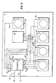
- Figure 1 shows a typical multiple channel data storage system 2 utilizing a different one of a plurality of low speed data storage units 4 for each data storage channel.
- Any number of the low speed data storage units 4 can be used, depending upon the desired data transfer speed requirements selected, and any recurrently cyclical storage medium can be utilized effectively, such as a magnetically or optically recorded disc or drum, or a semiconductive cyclomemory.
- the low speed data units 4 are shown to be of the magnetic disc type in Figure 1.
- the data retrieval rate will increase proportionally to the number of low speed data storage units 4 which are added to the system 2.
- the reason for this is that the data to be stored may be written over a smaller number of sectors on each disc, since the data is spread out among the low speed data units 4.
- an XOR data storage unit 6 is also included.
- the XOR data storage unit 6 is conveniently a unit which is substantially identical with the low speed data storage drive units 4.
- a data storage system multiplexer 8 divides incoming high speed data on a line 10 into four low speed data signals on respective multiplexer output lines 12, 14, 16 and 18.
- the data multiplexer 8 may be any well known configuration for converting a high speed data input to a plurality of low speed data outputs.
- the low speed data is recorded on the low speed data units 4 and is also read as it is written.
- the read data from each of the low speed data storage units 4 is transferred to an XOR circuit 20 via low speed data storage unit output lines 22, 24, 26 and 28 respectively.
- the XOR circuit 20 may use any well known configuration to provide a bit-by-bit XOR relationship for the read data transferred from each of the low speed data storage units 4 on the lines 22, 24, 26 and 28, respectively.
- the XOR circuit 20 provides an XOR output signal representing this bit-by-bit XOR comparison to the XOR data drive 6 via an XOR output line 30.
- a high speed data signal on the line 10 is converted by the multiplexer 8 into four low speed data signals, which low speed signals are transferred to each of the low speed data storage units 4 via the multiplexer output lines 12, 14, 16 and 18 respectively.
- the low speed data storage units 4 are synchronized with each other so that data transfers to and storage in the low speed data storage units 4 are retrievable with some degree of reliability.
- the four low speed data signals written on the low speed data storage units 4 are read from the low speed data storage units 4 as they are written, and the read signals are transferred to the XOR circuit 20 from each one of the low speed data storage units 4 via the XOR input lines 22, 24, 26 and 28 respectively.
- the XOR circuit 20 performs a bit-by-bit XOR comparison on the received low speed read signals and produces the XOR output signal, and transfers it to the XOR data storage unit 6 via the XOR output line 30.
- the known procedures for computing the XOR relationship in the XOR circuit 20 involve a significant delay period.
- the computational delay involved in producing the XOR output signal on the line 30 prevents the XOR output signal from being recorded in phase with the corresponding low speed data written on the low speed data storage units 4 from which the XOR data is generated.
- the XOR data read from the XOR data storage unit 6 be processed in synchronization with the low speed data read from the low speed data storage units 4 when data is to be retrieved from storage. Therefore, the XOR data may be written in a skewed relationship relative to its corresponding low speed data, as long as the read XOR data is properly synchronized with its corresponding low speed read data when retrieved from storage. The XOR data may then be written in the XOR data storage unit 6 as soon as the computation of the XOR data is complete. Consequently, the XOR latency interval is effectively reduced to the delay incurred with the XOR data computation alone. By shifting the synchronization process from the data writing stage to the data reading stage, the duration of the data write process is substantially reduced.
- the synchronization of the low speed read data from the low speed storage units 4 with the corresponding XOR read data from the XOR data storage unit 6 may be achieved with a variety of methods and circuit configurations.
- the low speed data read from the low speed data storage units 4 is transferred to a four channel digital delay circuit 32 via delay circuit input lines 34, 36, 38 and 40, which are respectively fed by the XOR input lines 22, 24, 26 and 28.
- the four channel delay circuit 32 includes a delay for each of its channels which is sufficient to synchronize the respective low speed read data passing through it with the corresponding XOR read data. The delay will approximate the computational delay required to generate the XOR data which has been written.
- the XOR circuit 20 computational delay will be somewhat less than one sector interval, or 238 microseconds.
- a digital delay circuit 32 which includes a 238 microsecond delay for each of its four channels will be sufficient to synchronize the respective low speed read data from the low speed data storage units 4 with the XOR read data from the XOR data storage unit 6.
- the digital delay circuit 32 may use any well known configuration for the selected delay, such as digital delay lines.
- Each of the four read data outputs from the four channel digital delay circuit 32 are transferred to a data storage system demultiplexer 42 via the demultiplexer input lines 44, 46, 48 and 50 respectively.
- the read data output from the XOR data storage unit 6 is also transferred to the demultiplexer 42 via an XOR data output line 52.
- the demultiplexer 42 processes the four delayed low speed read data signals received on the lines 44, 46, 48 and 50 to convert them to a single high speed data output signal, which high speed data output signal appears on a demultiplexer output line 54.
- the demultiplexer 42 also includes error detection and correction circuitry which senses any errors in the incoming low speed read data on the lines 44, 46, 48 and 50, and corrects the error-containing low speed read data with the XOR read data on the line 52.
- the write process duration for this low speed data on the low speed drives 4 is 238 microseconds.
- the XOR circuit 20 immediately retrieves the written low speed data on each of the low speed data storage units 4 via the lines 22, 24, 26 and 28, respectively, and computes the corresponding XOR data as described above.
- the XOR computational latency for the XOR circuit 20 is a variable which depends upon the specific configuration of the XOR circuit 20 which is adapted, this XOR computational latency is easily reduced to a fraction of the duration of the corresponding data from which it is computed, or less than 238 microseconds, in this instance.
- the XOR data is then transferred to the XOR data storage unit 6 via the line 30 for writing onto its corresponding medium with a skew corresponding to the duration of the XOR computational process, which is less than 238 microseconds, as explained above. Therefore, the complete write process can be completed in less than 476 microseconds.
- the total duration of the read process for the above described written low speed data and corresponding XOR data is only the interval between the beginning of the low speed data and the end of the corresponding skewed XOR data.
- the total read process time is the same as described above, less than 476 microseconds.
- the digital delay circuit 32 may be deleted if the XOR read data signal from the line 52 is otherwise advanced relative to the low speed read data signals on the lines 34, 36, 38 and 40.
- the multiple channel digital storage system 2 may be arranged as described above in connection with Figure 1, but the XOR data storage unit 6 is modified to provide an XOR read data signal which is advanced by the desired delay relative to the low speed read data signals from the low speed data storage units 4 on the lines 44, 46, 48 and 50, such as by relatively advancing the position of the read transducer in the XOR data storage unit 6 compared to the respective read transducers in the low speed data storage units 4.
- the lines 44, 46, 48 and 50 feed the low speed read data signals directly into the demultiplexer 42 from the low speed data storage units 4, since the synchronization of the low speed read data signals with the XOR read data signal is accomplished with repositioning of the read head in the XOR data storage unit 6.
- This embodiment of the invention allows the XOR data to be read simultaneously with the corresponding low speed data, so that the total read process duration, for the example described above in connection with the preferred embodiment of the invention, is only 238 microseconds.
- this embodiment requires that a special offset read head configuration be used in the XOR data storage medium 6.
- the storage medium in the XOR data storage unit 6 may be allowed to advance the corresponding positions of the storage media in each of the low speed data storage units 4 during the read process by an amount corresponding to the desired delay. So too, the storage media in the low speed data storage units 4 may each be retarded relative to the position of the storage medium in the XOR data storage unit 6 during the read process by an amount corresponding to the desired delay.
- the above described procedures allow the XOR data to be written as soon as possible after the corresponding low speed multiplexed data is written, and yet retrieved in synchronization during the read process.
- the writing speed of the entire multiple channel data storage system 2 is enhanced.
- the write process may be completed within the interval of less than one storage medium revolution, for a disc or drum drive, and typically within an interval of less than two data field sectors of one revolution.
- the total required duration of the write process is the actual data write interval of 238 microseconds plus the XOR latency, which is an integer fraction of the sector period equal to, or higher than, the computational interval required for the XOR data corresponding to the multiple channel low speed data.
- This XOR computational interval is a factor which is variable, and depends upon specific implementation, as explained above, but it is easily implemented as less than one sector period.
- the XOR data will be written with a skew of one sector period or less, rather than one complete revolution later, or 16.6 milliseconds later for the example described above, according to procedures of the prior art.
Landscapes
- Engineering & Computer Science (AREA)
- Signal Processing (AREA)
- Signal Processing For Digital Recording And Reproducing (AREA)
- Time-Division Multiplex Systems (AREA)
Applications Claiming Priority (2)
| Application Number | Priority Date | Filing Date | Title |
|---|---|---|---|
| US325281 | 1989-03-17 | ||
| US07/325,281 US5022030A (en) | 1989-03-17 | 1989-03-17 | Skewed XOR data storage process |
Publications (2)
| Publication Number | Publication Date |
|---|---|
| EP0393821A2 true EP0393821A2 (de) | 1990-10-24 |
| EP0393821A3 EP0393821A3 (de) | 1992-10-07 |
Family
ID=23267210
Family Applications (1)
| Application Number | Title | Priority Date | Filing Date |
|---|---|---|---|
| EP19900301980 Withdrawn EP0393821A3 (de) | 1989-03-17 | 1990-02-23 | Prozess zur Datenspeicherung mit Fehlerprüfung mittels exclusiv-oder mit Zeitverschiebung |
Country Status (4)
| Country | Link |
|---|---|
| US (1) | US5022030A (de) |
| EP (1) | EP0393821A3 (de) |
| JP (1) | JPH0322268A (de) |
| CA (1) | CA2010936A1 (de) |
Families Citing this family (2)
| Publication number | Priority date | Publication date | Assignee | Title |
|---|---|---|---|---|
| US5271012A (en) * | 1991-02-11 | 1993-12-14 | International Business Machines Corporation | Method and means for encoding and rebuilding data contents of up to two unavailable DASDs in an array of DASDs |
| US6732201B2 (en) * | 2001-12-17 | 2004-05-04 | Lsi Logic Corporation | Hardware speed selection behind a disk array controller |
Family Cites Families (7)
| Publication number | Priority date | Publication date | Assignee | Title |
|---|---|---|---|---|
| US3303482A (en) * | 1963-02-25 | 1967-02-07 | Rca Corp | Redundant recording system with parity checking |
| US4528666A (en) * | 1983-01-03 | 1985-07-09 | Texas Instruments Incorporated | Memory system with built in parity |
| FR2561428B1 (fr) * | 1984-03-16 | 1986-09-12 | Bull Sa | Procede d'enregistrement dans une memoire a disques et systeme de memoire a disques |
| CA1263194A (en) * | 1985-05-08 | 1989-11-21 | W. Daniel Hillis | Storage system using multiple mechanically-driven storage units |
| US4833655A (en) * | 1985-06-28 | 1989-05-23 | Wang Laboratories, Inc. | FIFO memory with decreased fall-through delay |
| DE3866902D1 (de) * | 1987-03-10 | 1992-01-30 | Siemens Ag | Verfahren und einrichtung zur steuerung der fehlerkorrektur innerhalb einer datenuebertragungssteuerung bei von bewegten peripheren speichern, insbesondere plattenspeichern, eines datenverarbeitungssystems gelesenen daten. |
| CA1296103C (en) * | 1987-06-02 | 1992-02-18 | Theodore Jay Goodlander | High-speed, high capacity, fault-tolerant, error-correcting storage system |
-
1989
- 1989-03-17 US US07/325,281 patent/US5022030A/en not_active Expired - Lifetime
-
1990
- 1990-02-23 EP EP19900301980 patent/EP0393821A3/de not_active Withdrawn
- 1990-02-26 CA CA002010936A patent/CA2010936A1/en not_active Abandoned
- 1990-03-16 JP JP2066754A patent/JPH0322268A/ja active Pending
Also Published As
| Publication number | Publication date |
|---|---|
| EP0393821A3 (de) | 1992-10-07 |
| JPH0322268A (ja) | 1991-01-30 |
| US5022030A (en) | 1991-06-04 |
| CA2010936A1 (en) | 1990-09-17 |
Similar Documents
| Publication | Publication Date | Title |
|---|---|---|
| US4275457A (en) | Apparatus and method for receiving digital data at a first rate and outputting the data at a different rate | |
| CN1021092C (zh) | 信息信号的记录、重放方法及装置 | |
| US4353130A (en) | Device for processing serial information which includes synchronization words | |
| US3641534A (en) | Intrarecord resynchronization in digital-recording systems | |
| US3708783A (en) | Interchannel time displacement correction method and apparatus | |
| US5022030A (en) | Skewed XOR data storage process | |
| US3710358A (en) | Data storage system having skew compensation | |
| JPS60145566A (ja) | デ−タ記録再生方式 | |
| KR100283144B1 (ko) | 디지털 기록/재생장치 | |
| JP2581121B2 (ja) | スキュー補正回路 | |
| JPS59121608A (ja) | 同期方式 | |
| US3747079A (en) | Reducing dead-tracking in recording systems | |
| JPS61134969A (ja) | デ−タ記録方式 | |
| JPS62208465A (ja) | デ−タ記録再生方式 | |
| JPS6386160A (ja) | 磁気記録方法 | |
| JP3271073B2 (ja) | 磁気再生装置 | |
| RU2029383C1 (ru) | Способ магнитной записи цифровой информации | |
| JPS628369A (ja) | デ−タ読取方式 | |
| JPH0419875A (ja) | 情報記録再生装置 | |
| JPS6253097B2 (de) | ||
| JP4247651B2 (ja) | 情報処理装置、情報記録媒体及び情報の伝送方法 | |
| JPH03173975A (ja) | 信号抽出方法および信号抽出装置 | |
| JPS5819768A (ja) | 回転形外部記憶装置 | |
| JPS5830651B2 (ja) | デ−タ検出方式 | |
| JPS6353629B2 (de) |
Legal Events
| Date | Code | Title | Description |
|---|---|---|---|
| PUAI | Public reference made under article 153(3) epc to a published international application that has entered the european phase |
Free format text: ORIGINAL CODE: 0009012 |
|
| 17P | Request for examination filed |
Effective date: 19900302 |
|
| AK | Designated contracting states |
Kind code of ref document: A2 Designated state(s): AT BE CH DE DK ES FR GB GR IT LI LU NL SE |
|
| PUAL | Search report despatched |
Free format text: ORIGINAL CODE: 0009013 |
|
| AK | Designated contracting states |
Kind code of ref document: A3 Designated state(s): AT BE CH DE DK ES FR GB GR IT LI LU NL SE |
|
| 17Q | First examination report despatched |
Effective date: 19940317 |
|
| STAA | Information on the status of an ep patent application or granted ep patent |
Free format text: STATUS: THE APPLICATION IS DEEMED TO BE WITHDRAWN |
|
| 18D | Application deemed to be withdrawn |
Effective date: 19940728 |