EP0394590A2 - Transistor à effet de champ et méthode de fabrication d'un transistor à effet de champ - Google Patents
Transistor à effet de champ et méthode de fabrication d'un transistor à effet de champ Download PDFInfo
- Publication number
- EP0394590A2 EP0394590A2 EP89312165A EP89312165A EP0394590A2 EP 0394590 A2 EP0394590 A2 EP 0394590A2 EP 89312165 A EP89312165 A EP 89312165A EP 89312165 A EP89312165 A EP 89312165A EP 0394590 A2 EP0394590 A2 EP 0394590A2
- Authority
- EP
- European Patent Office
- Prior art keywords
- insulating film
- semiconductor device
- etching
- source
- metal
- Prior art date
- Legal status (The legal status is an assumption and is not a legal conclusion. Google has not performed a legal analysis and makes no representation as to the accuracy of the status listed.)
- Granted
Links
Images

Classifications
-
- H—ELECTRICITY
- H10—SEMICONDUCTOR DEVICES; ELECTRIC SOLID-STATE DEVICES NOT OTHERWISE PROVIDED FOR
- H10D—INORGANIC ELECTRIC SEMICONDUCTOR DEVICES
- H10D30/00—Field-effect transistors [FET]
- H10D30/01—Manufacture or treatment
- H10D30/015—Manufacture or treatment of FETs having heterojunction interface channels or heterojunction gate electrodes, e.g. HEMT
-
- H—ELECTRICITY
- H10—SEMICONDUCTOR DEVICES; ELECTRIC SOLID-STATE DEVICES NOT OTHERWISE PROVIDED FOR
- H10D—INORGANIC ELECTRIC SEMICONDUCTOR DEVICES
- H10D30/00—Field-effect transistors [FET]
- H10D30/40—FETs having zero-dimensional [0D], one-dimensional [1D] or two-dimensional [2D] charge carrier gas channels
- H10D30/47—FETs having zero-dimensional [0D], one-dimensional [1D] or two-dimensional [2D] charge carrier gas channels having two-dimensional [2D] charge carrier gas channels, e.g. nanoribbon FETs or high electron mobility transistors [HEMT]
- H10D30/471—High electron mobility transistors [HEMT] or high hole mobility transistors [HHMT]
- H10D30/475—High electron mobility transistors [HEMT] or high hole mobility transistors [HHMT] having wider bandgap layer formed on top of lower bandgap active layer, e.g. undoped barrier HEMTs such as i-AlGaN/GaN HEMTs
- H10D30/4755—High electron mobility transistors [HEMT] or high hole mobility transistors [HHMT] having wider bandgap layer formed on top of lower bandgap active layer, e.g. undoped barrier HEMTs such as i-AlGaN/GaN HEMTs having wide bandgap charge-carrier supplying layers, e.g. modulation doped HEMTs such as n-AlGaAs/GaAs HEMTs
-
- H—ELECTRICITY
- H10—SEMICONDUCTOR DEVICES; ELECTRIC SOLID-STATE DEVICES NOT OTHERWISE PROVIDED FOR
- H10D—INORGANIC ELECTRIC SEMICONDUCTOR DEVICES
- H10D30/00—Field-effect transistors [FET]
- H10D30/60—Insulated-gate field-effect transistors [IGFET]
- H10D30/67—Thin-film transistors [TFT]
- H10D30/6729—Thin-film transistors [TFT] characterised by the electrodes
- H10D30/6737—Thin-film transistors [TFT] characterised by the electrodes characterised by the electrode materials
- H10D30/6738—Schottky barrier electrodes
-
- H—ELECTRICITY
- H10—SEMICONDUCTOR DEVICES; ELECTRIC SOLID-STATE DEVICES NOT OTHERWISE PROVIDED FOR
- H10D—INORGANIC ELECTRIC SEMICONDUCTOR DEVICES
- H10D30/00—Field-effect transistors [FET]
- H10D30/60—Insulated-gate field-effect transistors [IGFET]
- H10D30/67—Thin-film transistors [TFT]
- H10D30/674—Thin-film transistors [TFT] characterised by the active materials
- H10D30/675—Group III-V materials, Group II-VI materials, Group IV-VI materials, selenium or tellurium
-
- H—ELECTRICITY
- H10—SEMICONDUCTOR DEVICES; ELECTRIC SOLID-STATE DEVICES NOT OTHERWISE PROVIDED FOR
- H10D—INORGANIC ELECTRIC SEMICONDUCTOR DEVICES
- H10D30/00—Field-effect transistors [FET]
- H10D30/80—FETs having rectifying junction gate electrodes
- H10D30/87—FETs having Schottky gate electrodes, e.g. metal-semiconductor FETs [MESFET]
- H10D30/877—FETs having Schottky gate electrodes, e.g. metal-semiconductor FETs [MESFET] having recessed gate electrodes
-
- H—ELECTRICITY
- H10—SEMICONDUCTOR DEVICES; ELECTRIC SOLID-STATE DEVICES NOT OTHERWISE PROVIDED FOR
- H10D—INORGANIC ELECTRIC SEMICONDUCTOR DEVICES
- H10D64/00—Electrodes of devices having potential barriers
- H10D64/01—Manufacture or treatment
- H10D64/012—Manufacture or treatment of electrodes comprising a Schottky barrier to a semiconductor
- H10D64/0124—Manufacture or treatment of electrodes comprising a Schottky barrier to a semiconductor to Group III-V semiconductors
- H10D64/0125—Manufacture or treatment of electrodes comprising a Schottky barrier to a semiconductor to Group III-V semiconductors characterised by the sectional shape, e.g. T or inverted T
-
- H—ELECTRICITY
- H10—SEMICONDUCTOR DEVICES; ELECTRIC SOLID-STATE DEVICES NOT OTHERWISE PROVIDED FOR
- H10D—INORGANIC ELECTRIC SEMICONDUCTOR DEVICES
- H10D64/00—Electrodes of devices having potential barriers
- H10D64/20—Electrodes characterised by their shapes, relative sizes or dispositions
- H10D64/27—Electrodes not carrying the current to be rectified, amplified, oscillated or switched, e.g. gates
- H10D64/311—Gate electrodes for field-effect devices
- H10D64/411—Gate electrodes for field-effect devices for FETs
-
- H—ELECTRICITY
- H10—SEMICONDUCTOR DEVICES; ELECTRIC SOLID-STATE DEVICES NOT OTHERWISE PROVIDED FOR
- H10D—INORGANIC ELECTRIC SEMICONDUCTOR DEVICES
- H10D64/00—Electrodes of devices having potential barriers
- H10D64/60—Electrodes characterised by their materials
- H10D64/62—Electrodes ohmically coupled to a semiconductor
-
- H—ELECTRICITY
- H10—SEMICONDUCTOR DEVICES; ELECTRIC SOLID-STATE DEVICES NOT OTHERWISE PROVIDED FOR
- H10D—INORGANIC ELECTRIC SEMICONDUCTOR DEVICES
- H10D64/00—Electrodes of devices having potential barriers
- H10D64/60—Electrodes characterised by their materials
- H10D64/64—Electrodes comprising a Schottky barrier to a semiconductor
-
- H—ELECTRICITY
- H10—SEMICONDUCTOR DEVICES; ELECTRIC SOLID-STATE DEVICES NOT OTHERWISE PROVIDED FOR
- H10D—INORGANIC ELECTRIC SEMICONDUCTOR DEVICES
- H10D62/00—Semiconductor bodies, or regions thereof, of devices having potential barriers
- H10D62/80—Semiconductor bodies, or regions thereof, of devices having potential barriers characterised by the materials
- H10D62/85—Semiconductor bodies, or regions thereof, of devices having potential barriers characterised by the materials being Group III-V materials, e.g. GaAs
Definitions
- the present invention relates to a semiconductor device and a production method thereof, and more particularly to those of high electron mobility transistors (HEMT) and metal semiconductor field effect transistors (MESFET).
- HEMT high electron mobility transistors
- MESFET metal semiconductor field effect transistors
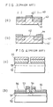
- Figures 2(a) to 2(d) are cross-sectional views showing process steps for producing a prior art semiconductor device.
- reference numeral 1 designates a semi-insulating GaAs substrate.
- An undoped GaAs layer 2 of about 5000 angstroms thickness is produced on the substrate 1.
- Two dimensional electron gas 3 are produced at an upper portion of the undoped GaAs layer 2.
- An n type AlGaAs layer 4 having a film thickness of about 1000 angstroms and impurity concentration of about 3 ⁇ 1017 cm ⁇ 3 is disposed on the undoped GaAs layer 2.
- n type GaAs layer 5 of about 2000 angstroms thickness and impurity concentration of about 3 ⁇ 1018 cm ⁇ 3 is disposed on the n type AlGaAs layer 4.
- a source electrode 6 and a drain electrode 7 are disposed on the n type GaAs layer 5.
- Reference numeral 8 designates a drain electrode production photoresist pattern and reference numeral 9 designates a gate electrode.
- the device will operate as follows.
- Electrons are supplied from the n type AlGaAs layer 4 to the undoped GaAs layer 2 and two dimensional electron gas 3 are generated at the undoped GaAs layer 2.
- the movement of these two-dimensional electron gas 3 are controlled by the gate electrode 9, and the current flowing between the drain electrode 6 and the source electrode 7 are thus controlled. Since the two-dimensional electron gas 3 move in the undoped GaAs layer 2, they are not scattered by impurities. Therefore, an FET of quite low noise characteristics is obtained.
- an epitaxy growth structure shown in figure 2(a) is produced by such as molecular beam epitaxy (MBE) or metal organic chemical vapor deposition (MOCVD).
- MBE molecular beam epitaxy
- MOCVD metal organic chemical vapor deposition
- a source and a drain electrode 6 and 7 are produced thereon by vapor deposition and lift-off.
- a gate electrode production photoresist pattern 8 is produced, and a recess is produced at the n type GaAs substrate 5 by a wet etching using such as sulfuric acid or tartaric acid etchant with using this photoresist pattern 8 as a mask.
- a gate electrode 9 is produced at the recess by vapor deposition and lift-off, thereby completing a device.
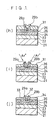
- FIG 3 shows another prior art GaAs MESFET disclosed in Japanese Patent Laid-open Publication No. Sho. 63-36577.
- indiums ions 40 are ion implanted into a GaAs semi-insulating substrate 41 on which an active layer 42 is produced and an annealing is executed thereto thereby to produce an In x Ga 1-x As layer 43 whose energy band gap is gradually lower as is closer to the surface.
- a metal layer is produced thereon, thereby producing source/drain electrodes 44 capable of providing non-alloying ohmic contact on the n+ type InGaAs layers 43 without conducting alloying.
- FIG 4 shows still another prior art GaAs MESFET disclosed in Japanese Patent Laid-open Publication No. Sho. 60-50967.
- an n+ type Ge thin layer 51 having the same function as the above-described n+ type InGaAs layer, that is, that capable of providing non-alloying ohmic contact source/drain electrodes, is laminated on an active layer 52, the Ge layer 51 is selectively etched (over-etched in the transverse direction) from the gate aperture portion of the insulating film for spacer 53 which is produced on the Ge layer 51, and a gate 54 is produced on the exposed surface of the etched portion.
- the insulating film for spacer 53 is photolithographied at the both external side portions of the gate aperture portion, and source and drain electrodes 55 and 56 are produced thereon.
- the effective interval between the source and gate can be controlled, and further, the source, gate, and drain electrodes can be produced from the same material at the same time, thereby simplifying the production process.
- the fine patterning of the gate cannot be conducted without the increase of the gate resistance. Furthermore, since the production of the source/drain electrodes is independently conducted by photolithography after the production of the gate aperture portion, the production of the source/drain electrodes is not conducted self-aligningly with the gate electrode, and there arises difficulty in sufficient reduction of the source series resistance.
- Another object of the present invention is to provide a semiconductor device superior in the uniformity and the reproducibility.
- Still another object of the present invention is to provide a method of producing such a semiconductor device.
- a T-shaped fine pattern gate is produced with utilizing an L-shaped insulating film and a reversely L-shaped insulating film.
- the increase in the gate resistance is suppressed and the gate is fine patterned.
- the gate electrode and the source/drain electrodes are position determined with providing a short distance therebetween, thereby enabling reduction in the source series resistance.
- An n+ type InGaAs layer is provided at an upper surface of the device, thereby enabling to produce source and drain electrodes of non-alloying ohmic contact and enabling to produce a gate electrode comprising the same metal material as that of the source and drain electrodes, thereby enhancing the reliability of a device.
- the source series resistance can be lowered without conducting selective etching of n type GaAs, thereby enabling to obtain a HEMT or MESFET device superior in the uniformity and the reproducibility of the current value and the pinch-off voltage.
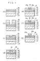
- Figures 1(a) to (j) are cross-sectional views showing a production method of a HEMT according to an embodiment of the present invention.
- reference numeral 21 designates a semi-insulating GaAs substrate.
- An undoped GaAs layer 22 having a film thickness of about 5000 angstroms is produced on the substrate 21.
- Two dimensional electron gas 23 are generated at an upper portion of the undoped GaAs layer 22.
- An n type AlGaAS layer 24 having a film thickness of about 1000 angstroms and impurity concentration of about 3 ⁇ 1017 cm ⁇ 3 is produced on the undoped GaAs layer 22.
- n type GaAs layer 25 having a film thickness of about 0 to 500 angstroms and impurity concentration of about 3 ⁇ 1018 cm ⁇ 3 is produced on the n type AlGaAs layer 24.
- Reference numeral 27 designates a first kind of insulating film comprising SiO having a film thickness of about 2000 angstroms.
- Reference numeral 28 designates a photoresist pattern for processing the first kind of insulating film 27.
- Reference numeral 29 designates a second kind of insulating film comprising SiN having a film thickness of 1500 angstroms.
- Reference numeral 30 designates a side wall produced of the first insulating film comprising SiO.
- Reference numeral 31 designates laminated metal of Ti/Mo/Au from below.
- Reference numeral 32 designates a gate electrode
- reference numeral 33 designates a drain electrode
- reference numeral 34 designates a source electrode.
- an epitaxy growth structure shown in figure 1(a) is produced by such as molecular beam epitaxy or metal organic chemical vapor deposition method.
- the first kind of insulating film 27 comprising SiO is produced on the entire surface of wafer to a thickness of about 2000 angstroms, and a photoresist pattern 28 is produced thereon, and thereafter, the first kind of insulating film 27 is processed by such as reactive ion etching (generally referred to as "RIE") using gas such as C2F6 + CHF3 + O2 + He with using the photoresist pattern 28 as a mask, thereby producing a groove of width below about 1 micron.
- RIE reactive ion etching
- a second kind of insulating film 29 comprising SiN is produced on the entire surface to a thickness of about 1500 angstroms.
- a first kind of insulating film comprising SiO is produced on the entire surface, and a portion thereof is etched by an etching such as RIE using C2F6 + CHF3 + O2 + He gas, and a side wall 30 comprising the first kind of insulating film is produced at the side surface of the second kind of insulating film 29.
- the second kind of insulating film 29 on the first kind of insulating film 27 is removed by an etching such as RIE.
- RIE that using CHF3 + O2 gas is used.
- the etching conditions including such as substrate temperature and mixing ratio of gas that would etch only the second kind of insulating film 29 and not etch the first kind of insulating films 27 and 30 are selected.
- the n+ type InGaAs layer 26 is selectively etched against the n type GaAs layer 25 by an etching solution such as boiled conc HCl.
- metal 31 comprising such as Ti/Mo/Au, Ti/Au, or Ti/Pt/Au from below is plated on the entire surface, and thereafter, as shown in figure 1(i), the excess metal is removed by diagonal direction ion milling using Ar gas, with utilizing the L-shaped and reversely L-shaped second kind of insulating films 29a and 29b.
- the source and drain electrodes 33, 34 and the gate electrode 32 are separated from each other, thereby completing a HEMT as shown in figure 1(j).
- a gate of fine pattern below about 0.5 micron width can be produced with suppressing an increase in the gate resistance, and further, the gate electrode and the source and drain electrodes can be self-aligningly position determined at short distance by the L-shaped and reversely L-shaped insulating films, thereby enabling to reduce the source series resistance.
- the n+ type InGaAs layer is provided at the most upper layer of the device and the source and drain electrodes are capable of being in non-alloying ohmiccontact with the n+ type InGaAs layer, the common use of the metal material through the source/drain electrode and the gate electrode is realized, thereby simplifying the production process and enhancing the reliability of a device.
- the source series resistance can be reduced without conducting recess etching of n type GaAs, thereby enabling to obtain a device superior in the uniformity and reproducibility of current value and pinch-off voltage.
- GaAs series HEMT While in the above-illustrated embodiment a GaAs series HEMT is described, the present invention may be also applied to GaAs series MESFET. Furthermore, the present invention may be also applied to InP series HEMT or MESFET.
- a T-shaped gate is produced by utilizing an L-shaped and reversely L-shaped insulating film and a side wall of the insulating film, the gate can be fine patterned with suppressing the increase in the gate resistance.
- the gate electrode and the source and drain electrodes can be self-aligningly position determined with providing a short distance therebetween via the L-shaped and reversely L-shaped insulating film. Therefore, the source series resistance can be reduced.
- n+ type InGaAs layer is provided at the most upper surface of the device and the source and drain electrodes are capable of being in non-alloying ohmic contact, common use of the metal material through the source/drain electrodes and the gate electrode is realized, thereby simplifying the fabrication process and enhancing the device reliability.
- the source series resistance can be reduced without conducting a recess etching of the n type GaAs, thereby obtaining a device superior in the uniformity and the reproducibility of the current value and the pinch-off voltage.
Landscapes
- Junction Field-Effect Transistors (AREA)
- Electrodes Of Semiconductors (AREA)
Applications Claiming Priority (2)
| Application Number | Priority Date | Filing Date | Title |
|---|---|---|---|
| JP1108232A JPH02285644A (ja) | 1989-04-27 | 1989-04-27 | 半導体装置およびその製造方法 |
| JP108232/89 | 1989-04-27 |
Publications (3)
| Publication Number | Publication Date |
|---|---|
| EP0394590A2 true EP0394590A2 (fr) | 1990-10-31 |
| EP0394590A3 EP0394590A3 (fr) | 1992-03-18 |
| EP0394590B1 EP0394590B1 (fr) | 1993-11-03 |
Family
ID=14479413
Family Applications (1)
| Application Number | Title | Priority Date | Filing Date |
|---|---|---|---|
| EP89312165A Expired - Lifetime EP0394590B1 (fr) | 1989-04-27 | 1989-11-23 | Transistor à effet de champ et méthode de fabrication d'un transistor à effet de champ |
Country Status (3)
| Country | Link |
|---|---|
| EP (1) | EP0394590B1 (fr) |
| JP (1) | JPH02285644A (fr) |
| DE (1) | DE68910509T2 (fr) |
Cited By (4)
| Publication number | Priority date | Publication date | Assignee | Title |
|---|---|---|---|---|
| EP0539688A3 (fr) * | 1991-10-29 | 1995-03-08 | Mitsubishi Electric Corp | |
| US5453627A (en) * | 1992-05-14 | 1995-09-26 | Nippon Telegraph And Telephone Corporation | Quantum interference device and complementary logic circuit utilizing thereof |
| EP3823036A1 (fr) * | 2019-11-18 | 2021-05-19 | Imec VZW | Procédé de mise à l'échelle d'une longueur de grille |
| CN115207109A (zh) * | 2021-04-07 | 2022-10-18 | 全新光电科技股份有限公司 | 半导体磊晶晶圆 |
Family Cites Families (1)
| Publication number | Priority date | Publication date | Assignee | Title |
|---|---|---|---|---|
| EP0283278B1 (fr) * | 1987-03-18 | 1993-06-23 | Fujitsu Limited | Composé semi-conducteur à contacts ohmiques sans alliage |
-
1989
- 1989-04-27 JP JP1108232A patent/JPH02285644A/ja active Pending
- 1989-11-23 DE DE89312165T patent/DE68910509T2/de not_active Expired - Fee Related
- 1989-11-23 EP EP89312165A patent/EP0394590B1/fr not_active Expired - Lifetime
Cited By (4)
| Publication number | Priority date | Publication date | Assignee | Title |
|---|---|---|---|---|
| EP0539688A3 (fr) * | 1991-10-29 | 1995-03-08 | Mitsubishi Electric Corp | |
| US5453627A (en) * | 1992-05-14 | 1995-09-26 | Nippon Telegraph And Telephone Corporation | Quantum interference device and complementary logic circuit utilizing thereof |
| EP3823036A1 (fr) * | 2019-11-18 | 2021-05-19 | Imec VZW | Procédé de mise à l'échelle d'une longueur de grille |
| CN115207109A (zh) * | 2021-04-07 | 2022-10-18 | 全新光电科技股份有限公司 | 半导体磊晶晶圆 |
Also Published As
| Publication number | Publication date |
|---|---|
| EP0394590A3 (fr) | 1992-03-18 |
| DE68910509D1 (de) | 1993-12-09 |
| JPH02285644A (ja) | 1990-11-22 |
| DE68910509T2 (de) | 1994-03-24 |
| EP0394590B1 (fr) | 1993-11-03 |
Similar Documents
| Publication | Publication Date | Title |
|---|---|---|
| US6627473B1 (en) | Compound semiconductor device with delta doped layer under etching stopper layer for decreasing resistance between active layer and ohmic electrode and process of fabrication thereof | |
| US4679311A (en) | Method of fabricating self-aligned field-effect transistor having t-shaped gate electrode, sub-micron gate length and variable drain to gate spacing | |
| US5538910A (en) | Method of making a narrow gate electrode for a field effect transistor | |
| WO2002031886A1 (fr) | Tgme integre monolithique a enrichissement/appauvrissement et procede de fabrication associe | |
| US6194747B1 (en) | Field effect transistor | |
| US6087207A (en) | Method of making pseudomorphic high electron mobility transistors | |
| KR100293010B1 (ko) | 전계효과트랜지스터및그의제조방법 | |
| JP2735718B2 (ja) | 化合物半導体装置及びその製造方法 | |
| US5231040A (en) | Method of making a field effect transistor | |
| US5939737A (en) | High-speed compound semiconductor device having a minimized parasitic capacitance and resistance | |
| JP3119248B2 (ja) | 電界効果トランジスタおよびその製造方法 | |
| JP3483716B2 (ja) | 半導体装置 | |
| EP0394590B1 (fr) | Transistor à effet de champ et méthode de fabrication d'un transistor à effet de champ | |
| JPH06260507A (ja) | 半導体装置及びその製造方法 | |
| US5837570A (en) | Heterostructure semiconductor device and method of fabricating same | |
| JP2000223504A (ja) | 電界効果型半導体装置およびその製造方法 | |
| EP0552763A2 (fr) | Dispositif formé d'un semi-conducteur composé avec une grille auto-alignée et la méthode de fabrication de ce dispositif | |
| KR100261461B1 (ko) | 비대칭 리쎄스 구조를 갖는 화합물반도체 소자의 제조 방법 | |
| JPH04291732A (ja) | 電界効果トランジスタの製造方法 | |
| JPH0817241B2 (ja) | 細線電界効果トランジスタ及びその製造方法 | |
| JPH06232168A (ja) | 電界効果トランジスタおよびその製造方法 | |
| JP3141931B2 (ja) | 電界効果トランジスタ | |
| JPH05275464A (ja) | 化合物半導体集積回路装置の製造方法 | |
| JPH0521473A (ja) | 電界効果トランジスタの製造方法 | |
| KR100554967B1 (ko) | 음성미분저항 억제용 부정합 고전자이동도 트랜지스터 및제조 방법 |
Legal Events
| Date | Code | Title | Description |
|---|---|---|---|
| PUAI | Public reference made under article 153(3) epc to a published international application that has entered the european phase |
Free format text: ORIGINAL CODE: 0009012 |
|
| AK | Designated contracting states |
Kind code of ref document: A2 Designated state(s): DE FR GB |
|
| 17P | Request for examination filed |
Effective date: 19901228 |
|
| PUAL | Search report despatched |
Free format text: ORIGINAL CODE: 0009013 |
|
| AK | Designated contracting states |
Kind code of ref document: A3 Designated state(s): DE FR GB |
|
| 17Q | First examination report despatched |
Effective date: 19930318 |
|
| GRAA | (expected) grant |
Free format text: ORIGINAL CODE: 0009210 |
|
| AK | Designated contracting states |
Kind code of ref document: B1 Designated state(s): DE FR GB |
|
| REF | Corresponds to: |
Ref document number: 68910509 Country of ref document: DE Date of ref document: 19931209 |
|
| ET | Fr: translation filed | ||
| PLBE | No opposition filed within time limit |
Free format text: ORIGINAL CODE: 0009261 |
|
| STAA | Information on the status of an ep patent application or granted ep patent |
Free format text: STATUS: NO OPPOSITION FILED WITHIN TIME LIMIT |
|
| 26N | No opposition filed | ||
| REG | Reference to a national code |
Ref country code: GB Ref legal event code: 746 Effective date: 19951026 |
|
| REG | Reference to a national code |
Ref country code: FR Ref legal event code: D6 |
|
| PGFP | Annual fee paid to national office [announced via postgrant information from national office to epo] |
Ref country code: FR Payment date: 19991109 Year of fee payment: 11 |
|
| PGFP | Annual fee paid to national office [announced via postgrant information from national office to epo] |
Ref country code: GB Payment date: 19991117 Year of fee payment: 11 |
|
| PGFP | Annual fee paid to national office [announced via postgrant information from national office to epo] |
Ref country code: DE Payment date: 19991129 Year of fee payment: 11 |
|
| PG25 | Lapsed in a contracting state [announced via postgrant information from national office to epo] |
Ref country code: GB Free format text: LAPSE BECAUSE OF NON-PAYMENT OF DUE FEES Effective date: 20001123 |
|
| GBPC | Gb: european patent ceased through non-payment of renewal fee |
Effective date: 20001123 |
|
| PG25 | Lapsed in a contracting state [announced via postgrant information from national office to epo] |
Ref country code: FR Free format text: LAPSE BECAUSE OF NON-PAYMENT OF DUE FEES Effective date: 20010731 |
|
| PG25 | Lapsed in a contracting state [announced via postgrant information from national office to epo] |
Ref country code: DE Free format text: LAPSE BECAUSE OF NON-PAYMENT OF DUE FEES Effective date: 20010801 |
|
| REG | Reference to a national code |
Ref country code: FR Ref legal event code: ST |