EP0394865A2 - Flache reflektierende optische Geräte - Google Patents
Flache reflektierende optische Geräte Download PDFInfo
- Publication number
- EP0394865A2 EP0394865A2 EP90107521A EP90107521A EP0394865A2 EP 0394865 A2 EP0394865 A2 EP 0394865A2 EP 90107521 A EP90107521 A EP 90107521A EP 90107521 A EP90107521 A EP 90107521A EP 0394865 A2 EP0394865 A2 EP 0394865A2
- Authority
- EP
- European Patent Office
- Prior art keywords
- substrate
- optical
- planar
- light
- fabricated
- Prior art date
- Legal status (The legal status is an assumption and is not a legal conclusion. Google has not performed a legal analysis and makes no representation as to the accuracy of the status listed.)
- Ceased
Links
- 230000003287 optical effect Effects 0.000 title claims abstract description 159
- 239000000758 substrate Substances 0.000 claims abstract description 137
- 239000000463 material Substances 0.000 claims description 10
- 238000005530 etching Methods 0.000 claims description 7
- 238000000151 deposition Methods 0.000 claims 4
- 238000000034 method Methods 0.000 abstract description 22
- 238000004519 manufacturing process Methods 0.000 abstract description 17
- 238000013459 approach Methods 0.000 description 13
- 239000011521 glass Substances 0.000 description 10
- 238000003384 imaging method Methods 0.000 description 9
- 230000008901 benefit Effects 0.000 description 8
- 239000004065 semiconductor Substances 0.000 description 7
- 238000003491 array Methods 0.000 description 6
- 239000011248 coating agent Substances 0.000 description 6
- 238000000576 coating method Methods 0.000 description 6
- 238000013461 design Methods 0.000 description 6
- 229910052782 aluminium Inorganic materials 0.000 description 4
- XAGFODPZIPBFFR-UHFFFAOYSA-N aluminium Chemical compound [Al] XAGFODPZIPBFFR-UHFFFAOYSA-N 0.000 description 4
- 230000006870 function Effects 0.000 description 4
- 230000013011 mating Effects 0.000 description 4
- JBRZTFJDHDCESZ-UHFFFAOYSA-N AsGa Chemical compound [As]#[Ga] JBRZTFJDHDCESZ-UHFFFAOYSA-N 0.000 description 3
- 229910001218 Gallium arsenide Inorganic materials 0.000 description 3
- XUIMIQQOPSSXEZ-UHFFFAOYSA-N Silicon Chemical compound [Si] XUIMIQQOPSSXEZ-UHFFFAOYSA-N 0.000 description 3
- 230000000694 effects Effects 0.000 description 3
- 238000010894 electron beam technology Methods 0.000 description 3
- 229920002120 photoresistant polymer Polymers 0.000 description 3
- 229910052710 silicon Inorganic materials 0.000 description 3
- 239000010703 silicon Substances 0.000 description 3
- 239000012780 transparent material Substances 0.000 description 3
- 241001156002 Anthonomus pomorum Species 0.000 description 2
- VYPSYNLAJGMNEJ-UHFFFAOYSA-N Silicium dioxide Chemical compound O=[Si]=O VYPSYNLAJGMNEJ-UHFFFAOYSA-N 0.000 description 2
- 229910021417 amorphous silicon Inorganic materials 0.000 description 2
- 201000009310 astigmatism Diseases 0.000 description 2
- 238000004891 communication Methods 0.000 description 2
- 238000007796 conventional method Methods 0.000 description 2
- 238000009792 diffusion process Methods 0.000 description 2
- 239000000428 dust Substances 0.000 description 2
- 238000005286 illumination Methods 0.000 description 2
- 238000007373 indentation Methods 0.000 description 2
- 239000013307 optical fiber Substances 0.000 description 2
- 230000008569 process Effects 0.000 description 2
- 238000012545 processing Methods 0.000 description 2
- 238000004544 sputter deposition Methods 0.000 description 2
- MZQZQKZKTGRQCG-UHFFFAOYSA-J thorium tetrafluoride Chemical compound F[Th](F)(F)F MZQZQKZKTGRQCG-UHFFFAOYSA-J 0.000 description 2
- 230000009471 action Effects 0.000 description 1
- 238000004026 adhesive bonding Methods 0.000 description 1
- 230000003679 aging effect Effects 0.000 description 1
- 230000004075 alteration Effects 0.000 description 1
- 230000001668 ameliorated effect Effects 0.000 description 1
- 239000006117 anti-reflective coating Substances 0.000 description 1
- 230000015572 biosynthetic process Effects 0.000 description 1
- 230000001447 compensatory effect Effects 0.000 description 1
- 230000008878 coupling Effects 0.000 description 1
- 238000010168 coupling process Methods 0.000 description 1
- 238000005859 coupling reaction Methods 0.000 description 1
- 230000007812 deficiency Effects 0.000 description 1
- 230000001419 dependent effect Effects 0.000 description 1
- 238000000609 electron-beam lithography Methods 0.000 description 1
- 239000004744 fabric Substances 0.000 description 1
- 239000000835 fiber Substances 0.000 description 1
- 239000012530 fluid Substances 0.000 description 1
- 230000003760 hair shine Effects 0.000 description 1
- 230000010354 integration Effects 0.000 description 1
- 230000003993 interaction Effects 0.000 description 1
- 230000007246 mechanism Effects 0.000 description 1
- 230000004048 modification Effects 0.000 description 1
- 238000012986 modification Methods 0.000 description 1
- 238000013139 quantization Methods 0.000 description 1
- 230000004044 response Effects 0.000 description 1
- 230000035882 stress Effects 0.000 description 1
- 230000009466 transformation Effects 0.000 description 1
- 238000000844 transformation Methods 0.000 description 1
- 238000007738 vacuum evaporation Methods 0.000 description 1
Images



Classifications
-
- G—PHYSICS
- G02—OPTICS
- G02B—OPTICAL ELEMENTS, SYSTEMS OR APPARATUS
- G02B6/00—Light guides; Structural details of arrangements comprising light guides and other optical elements, e.g. couplings
- G02B6/10—Light guides; Structural details of arrangements comprising light guides and other optical elements, e.g. couplings of the optical waveguide type
- G02B6/12—Light guides; Structural details of arrangements comprising light guides and other optical elements, e.g. couplings of the optical waveguide type of the integrated circuit kind
- G02B6/122—Basic optical elements, e.g. light-guiding paths
- G02B6/124—Geodesic lenses or integrated gratings
Definitions
- This relates to integrated optics for free space computing environments. More particularly, this relates to techniques for developing interacting arrays of optical elements that need not be aligned with cumbersome mechanical arrangements in order to realize free space computing.
- optical systems employ a variety of optical components, such as lenses and beam splitters, which are mounted and aligned by mechanical means.
- optical components such as lenses and beam splitters
- the alignment and the stability of these components become critical issues.
- the alignment problem becomes particularly severe when the required precision approaches the limits of conventional fine mechanics.
- the required precision is related to the size of the optical logic gates which are used to perform logic operations, such as AND and OR functions.
- the sizes of the optical logic devices that are currently investigated are in the range of a few microns or less. This means that the alignment tolerances for the optical components have to be in the submicron range.
- Conventional mechanical alignment of optical components is possible with a precision in the range of 10 microns. Below that range, conventional techniques become increasingly expensive. This means that for the purpose of building complex optical systems which require very precise mounting, alternative technique must be devised. The issue, then, is "How do we put all the components together with a submicron precision such that the resulting arrangement will stay stable despite influences such as temperature changes, mechanical stress, aging effects, etc.”.
- interconnections also present a challenge.
- the challenge in the semiconductor art results from the fact that electronic elements (e.g. transistors, resistors, paths, etc.) are basically planar devices and the interconnections between the electronic elements are restricted to planar paths. This is particularly troublesome for connections to and from the integrated circuits.
- the reason for that relates to the need to reach an edge of the integrated circuit and the need to provide sufficient current carrying capabilities to drive the signals on the input/output leads to the desired voltage levels in the presence of circuit capacitances.
- the Brenner et al. arrangement is similar to that of Goodman et al. in that both the light source and the detector are on the same exposed integrated circuit surface.
- the light is directed upwards toward a substrate that is held above the integrated circuit's exposed surface and which contains holograms at designated locations of the substrate.
- the holograms are at the surface of the substrate that faces the integrated circuit (the near-end surface).
- a mirrored surface is placed at the opposite surface of the substrate (the far-end surface).
- the light from an integrated circuit light source passes through the hologram of the substrate, reflects off the mirrored surface, and returns to the surface of the integrated circuit where an optical detector is situated (if the arrangement is aligned properly).
- the light that is reflected off the far-end surface is reflected off a mirrored portion on the near-end surface, and is reflected again off the far-end surface before it reaches the integrated circuit. This allows a lengthening of the optical path and offers certain flexibility in the positioning of the light detector vis-a-vis the light source.
- the above arrangements perhaps solve the problem of relaying signals to and from integrated circuits. They do not, however, solve the needs of an optical computing system. First, they do not obviate the need for alignment. The holograms and the mirrors in the above-described arrangements must be aligned precisely. Second, they address only the relatively simple process of sending an optical signal from one point and receiving it at another. They do not solve the problem of creating a circuit having optical elements that more generally interact with one another. Third, the above-described systems basically deal with one-to-one or one-to-many communications, whereas optical computing applications need to relay images (a collection of spots). The importance of this difference lies in the fact that a lens inverts the image. In the case of spot to spot communication that inversion is irrelevant to the detector and thus not considered. In the case of image manipulations, in contradistinction, one may not invert portions of the image with greatity.
- an optical circuit is any arrangement of optical elements such as mirrors, lenses, etc. that perform predefined transformations on optical signals.
- the substrate has one or two major surfaces and the elements are grown or fabricated on those surfaces using conventional integrated circuit manufacturing techniques. In such a circuit the relative positions of the optical elements are set by the fabricating mask.
- the fabricating masks may be generated by an electron beam writer which offers a position accuracy on the order of 0.1 micron.
- the mask can be as large as several inches in diameter.
- this invention provides reflective planar optical devices. These devices are created, in accordance with our invention, by including a reflective layer in direct contact with the optical planar devices that are fabricated on the substrates.
- the kernel of the reported advance in the art lies in our realization that different planar optical devices can be fabricated on a substrate, with a relative positioning of the devices being such that the devices interact optically with one another to form an optical circuit.
- the substrate is made of a transparent material, such as glass, and planar optical elements are fabricated on two surfaces of the substrate.
- the elements are arranged for light that enters the substrate to interact with the elements by "bouncing" within the substrate between the various lenses, beam splitters, mirrors, etc.
- To contain the light within the substrate, of the planar optical devices are covered with a reflective coating.
- the substrate upon which planar optical elements are fabricated can be opaque, and a transparent substrate is placed on top of the optical elements.
- the transparent substrate contains at least a mirrored surface, but it can also contain other and more complex planar optical elements in accordance with the aforementioned first embodiment of our invention.
- the advantage of the second embodiment lies in the fact that the first, opaque, substrate can be made of material that has desirable properties which are not found in transparent materials. For example, various devices such as optical detectors, lasers, etc. cannot presently be manufactured from transparent materials but can be manufactured from a semiconductor substrate.
- FIG. 1 depicts a typical 4-f imaging setup comprising an image 10 at a first plane, a lens 20 situated one focal distance away from image 10 and a phase grating plate 30 situated one focal distance away from lens 20 and two focal distances away from image 10.
- One more focal distance away from image 10 (coaxially with lens 20 and phase grating 30) there is lens 40 and still one more focal distance away from image 10, there is imaging plane 50.
- the optical setup of FIG. 1 is quite general since it can be used for simple imaging, but also for other applications in analog or digital data processing.
- this setup can be used to implement one stage of the perfect shuffle interconnection network following the teachings of Brenner and Huang in U.S. Patent Application Serial No. 296,284 filed January 11, 1989.
- Phase grating plate 30 can be designed to realize a simple beam splitter which results in the desired spatial shifting of one image at surface 50 with respect to the other. The shifting can be arranged (as described in the aforementioned application) to form the perfect shuffle arrangement.
- FIG. 1 arrangement can be realized with the arrangement depicted in FIGS. 2, and 7.
- FIG. 2 depicts, in a cross-sectional view, our basic idea of employing the VLSI techniques for fabricating planar optical components to form optical circuits that avoid the difficulties of optical component alignments.
- the substrate in FIG. 2 (60) is transparent.
- Incoming light, following path 61, is applied to planar lens 62 that is fabricated on the bottom surface of substrate 60.
- the outer surface of lens 62 (the surface away from the glass substrate) is coated with a reflective layer to make lens 62 a reflective lens.
- the light passing through planar lens 62 is reflected, therefore, and reaches the top surface of substrate 60 where a planar beam splitter 63 is fabricated.
- the outer surface of planar beam splitter 63 (the surface away from the glass substrate) is also coated with a reflective layer.
- the light passing through planar beam splitter 63 is reflected, therefore, and reaches the bottom surface of substrate 60 where a planar lens 64 is fabricated.
- Lens 64 is identical to lens 62. Light reflected off lens
- planar lens 62 as well as other planar optical devices can be fabricated using well known techniques. Still, one should clearly separate the concepts that relate to manufacturing of devices, and the concepts that teach the design of what should be manufactured. With respect to the former, conventional techniques are available for mass fabrication of semiconductor devices and, as indicated above, many of these techniques have been adopted for the manufacture of optical devices. As for the design of what to manufacture, interesting approaches are also available. Known approaches employ a bi-level realization of the needed optical response. One approach that I have employed is a multi-level fabrication technique which is, in effect, a digital embodiment of an analog design of a planar optical device. Growth, etching and diffusion are some of the different manufacturing techniques that are available.
- FIG. 4 depicts the cross-sectional view of our "planar multi-level optical lens" realization of the FIG. 3 optical device. This design can be used in the optical system of FIG. 2.
- the FIG. 4 realization grows the planar optical device on the substrate with a number of masks that is equal to log2 of the number of levels desired.
- the last step in the creation of the devices used in FIG. 2 is a reflective coating.
- the optical elements in the arrangement of FIG. 2 operate on signals traveling within the substrate. Accordingly, the reflective coating is on top of the grown structure. In applications where the our planar optical elements operate on signals that reach the optical element from outside the substrate, the reflective coating may be applied as the first layer of the substrate. These variations are shown in FIG. 5 where the reflective surfaces are marked by 66 and 67.
- FIG. 6 presents a lens realization that employs etching techniques rather than growth techniques.
- the reflective layer is the step that follows the formation of the lens. It may be noted in passing that the reflective surface on the FIG. 6 realization results a lens action for light reaching planar lens from outside the substrate as well as from inside the substrate.
- the path between lens 62 and beam splitter 63 is fairly short. This path can be lengthened as much as necessary by simply allowing the light beams to "bounce" a number of times off the top and bottom surfaces of the substrate.
- An example of this arrangement is depicted in FIG. 7.
- One attribute of the FIG. 7 embodiment, which is not directly related to the issue of path length, is that all of the complex planar optical devices whose structure and position relative to each other are critical are on the same surface of substrate 60.
- the other surface of substrate 60 can be a simple reflective surface or a blazed grating.
- FIG. 8 illustrates the principles of our invention when two or more substrates are used.
- substrate 70 is transparent whereas substrate 80 is opaque.
- incoming light arrives along path 61 from outside the arrangement. It passes through planar optical devices 71 through 79 before it exits along path 65.
- Optical devices 73, 76 and 78 are reflective planar optical devices of the type described above in connection with FIGS. 2 and 7. They are manufactured on the top side of substrate 70.
- Planar device 77 is a reflective planar optical device that is manufactured on the bottom side of substrate 70, which is the side that is mated with the top side of substrate 80.
- Devices 71 and 74 are also manufactured on the bottom side of substrate 70, but they are transmissive planar optical devices.
- devices 71 and 74 allow the light that is altered by the devices to reach substrate 80.
- substantial advantages can be derived by manufacturing most, if not all, of the position-sensitive optical devices on the sides of substrates 70 and 80 that are mated to each other.
- a reflective planar optical device is a device having some means for reflecting, such as a reflective coating, that is an integral part of the created optical device. It does not include, for example, a transmissive optical device manufactured on a transparent substrate, with a mirror on the opposite side of the substrate.
- a transmissive optical device manufactured on a transparent substrate, with a mirror on the opposite side of the substrate.
- a mirror is also an optical device. To differentiate between mirrors and more complex optical devices such as lenses, prisms, beam splitters, etc., the phrase "level A optical devices” will designate mirrors, "level B planar optical devices” will designate devices other than mirrors.
- Substrate 80 includes optical elements 72, 75, and 79. They are all either reflective planar optical devices, light detectors, or light emitters.
- the mating of substrates 80 and 70 presents two problems.
- the first problem is associated with the changes in refractive indices between substrate 70 and the air between substrates 70 and 80.
- the index of refraction of substrate 80 must also be taken into account.
- the problems associated with the index of refraction can be ameliorated by the use of index-matching fluid between substrates 70 and 80 or anti-reflective coatings on the surfaces.
- the second mating problem for substrates 70 and 80 is simply the alignment problem between the devices on substrate 70 and the devices on substrate 80. Note, for example, that the reflective device 72 on substrate 80 must be aligned properly with the transmissive device 71 on substrate 70.
- substrates 70 and 80 are mated through use of aligning elements that are fabricated into the substrates together with the fabrication of the optical devices. More specifically, the optical devices on substrate 70 are manufactured, as indicated above, through either etching, diffusion or growing techniques, or a combination of the above, to create protrusion and indentation structures in the surface of the substrates.
- substrates 70 and 80 can be mated with the accuracy that is available for manufacturing the planar optical devices in the first instance. This mating is depicted in FIG. 9, which is an enlarged view of the segment in the FIG. 7 arrangement that includes a portion of optical device 79 as well as the alignment structures 66.
- substrate 80 may be a silicon semiconductor substrate, a gallium arsenide substrate or, even, a silicon substrate upon which gallium arsenide is grown.
- phototransistors, LEDs, optical modulator devices and lasers can be manufactured. This allows light to be detected at the substrate, manipulated optically or even electronically, and regenerated with the same or another element on the substrate.
- FIG. 10 depicts one embodiment where optical device 81 in substrate 80 generates light, optical devices 82, 83 and 84 in substrate 70 interact with that light, and optical device 85 in substrate 80 detects light.
- substrate 80 it is possible for substrate 80 to have devices 81 and 85 physically mounted on the substrate, although some of the advantages described in connection with the mating of substrates 70 and 80 may be more difficult to realize.
- FIG. 11 illustrates an arrangement for an even larger optical system than the system of FIGS. 7, 8 and 10. It comprises substrates 91, 92, 93 and 94 that are mated in an arrangement that is akin to the placing of dominoes. In this arrangement, light travels through the substrates as illustrated by path 95. In the course of its travel, the light meanders through substrate 91, then passes through to substrate 92, then 93 and finally passes to substrate 94. The substrates are mated with the aid of alignment elements 95. The same effect can be obtained in an even more compact arrangement. That arrangement, depicted in FIG. 12, represents a folding of the FIG. 11 arrangement.
- FIG. 11 embodiment would include the position-sensitive optical devices only on the surfaces that mate different substrates.
- lens 20 and 40 would have to each be replaced with an array of lenslets.
- Each spot of image 10 would have to be relayed via a lenslet at position 20 to a lenslet at position 40 and then projected onto the corresponding point on output plane 50. This would complicate fabrication, create optical constraints and introduce spatial quantization noise such as crosstalk between adjacent spots.
- the optical arrangement consists of three layers.
- the top layer and the bottom layer are blazed gratings.
- the top layer redirects a light beam traveling under an oblique angle so that it is reflected under 90 degrees.
- the bottom layer redirects a light beam that travels under 90 degrees so that it is reflected under a corresponding oblique angle. In this manner, a light beam applied at a 90 degree angle to the bottom layer would reflect at an angle to the top layer, reflect again at 90 degrees to the the bottom layer, and so forth.
- the central layer in FIG. 22 contains optical devices such as lenses, beam splitters, etc. They are spaced far enough apart so that the light traveling at the oblique angle can pass between the optical devices, and close enough so that the light traveling at 90 degrees can pass through the devices.
- the top layer and the bottom layer contain windows which allows the light to enter and leave the arrangement.
- FIG. 22 can be fabricated in a number of ways. Employing the principles of this invention, however, the arrangement of FIG. 22 can be fabricated from two substrates 150 and 160. Both substrates contain one surface on which the blazed grating is fabricated. The other surface of one or both of the substrates can contain the optical elements necessary for implementing the optical function desired and, optionally, include the aligning means described in connection with FIGS. 8 and 9.
- a facsimile includes optical head that has the task of imaging one line of the original text or drawing onto a one-dimensional detector array.
- the detector array is typically a CCD line-scan camera.
- the de facto standard of the resolution for FAX applications is 300 dots per inch, which corresponds to a pixel diameter of approximately 85 microns, and 2400 pixels for an eight inch image line.
- the entire optical head of a FAX system can be created in a single unit.
- Two different optical approaches are possible for developing such an optical head arrangement: one, where the original image is subdivided into small but extended areas in the range 0.5-1 mm; and the other, where the original image is subdivided into areas equal to the pixel size so that each and every pixel has its own optical channel.
- lens 8 is a transmissive lens while lens 99 is a reflective lens.
- Device 101 is a mirror. Both lenses, as shown in FIG. 11, are fabricated on the bottom side of substrate 100. It should be realized, of course, those lenses can also be fabricated on the top surface of substrate 100, or on both the top and the bottom surfaces.
- the paper containing the image, by the way, is moving in the direction marked by the arrow x, from left to right.
- the diameter of lenses 98 and 99 is typically 1 mm.
- the working distance, w, between the moving papers and the lenses is typically 10 mm. This results in a relatively small angle ⁇ of approximately 5°, under the assumption that lenses 98 and 99 are of equal size without a space between them.
- the field of view of a lens is smaller than its diameter. Because of this, the lenses must be staggered spatially, as shown by line 130 in FIG. 15, if one wants to cover the entire line image. Of course, the staggering does not affect the performance of the system. It only requires a slight modification in the detector timing, in accordance with well established techniques.
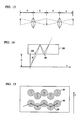
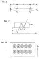
- FIG. 16 depicts the optical arrangement when an optical channel is devoted to each pixel.
- the folded version of the FIG. 16 arrangement is shown in FIG. 17.
- This arrangement is similar to one that uses a linear array of optical fibers where every fiber transmits the intensity of light coming from a single pixel.
- w a working distance
- the working distance must be as close to 0 as practicable, and that leads to problems, such as wear, dust, etc.
- the working distance can be between 1-10 mm.
- FIG. 17 approach One interesting aspect of the FIG. 17 approach is that double imaging is not necessary. This simplifies the optics, although in order to avoid crosstalk a collimated system as shown in FIG. 16 is suggested.
- the planar arrangement of the lenses in FIG. 17 is shown in FIG 18.
- the distance, t, between the two lenses in FIG. 16 is not critical and, therefore, the distance d between the lenses in FIGS. 17 and 18 is also not critical (other than being dependent on the angle ⁇ and the Thickness of the glass substrate).
- the complex planar optical devices can be fabricated on the surface of the substrate that is removed from the paper, to improve reliability.
- FIG. 19 presents the entire FAX optical head embodiment that includes the imaging light sources, the light focusing paths, and the detectors. More specifically, substrate 120 includes transmissive lenses 121 and 122, a reflective lens 123, a mirror 124, a light source 125 and a light detector 126. Each one of the depicted optical elements represents, of course, an entire row of elements as shown in FIG. 18. The only difficulty in realizing the arrangement of FIG. 7 lies in the creation of light sources 125 and detectors 126 on the glass substrate. The detectors can be manufactured by sputtering amorphous silicon directly on the glass substrate. The light sources, on the other hand, are more difficult to realize.
- LEDs and laser diodes are made of gallium arsenide and, currently, there are no known methods for integrating this material on quartz glass or on any other transparent substrate.
- both the light sources and the detectors can be either physically mounted on substrate 120 or, in the alternative, the FAX optical head can be constructed with two mated substrates as depicted in FIG. 20.
- the bottom substrate, 120 is transparent and it includes the lenses.
- the top substrate, 130 is the one that contains the light sources and detectors.
- FIG. 21 Still another embodiment is presented in FIG. 21.
- the optical FAX head in that it contains only a single glass substrate, only two arrays of reflective planar lenses, one mirrored surface, a light emitting array that is constructed separately and applied (e.g., glued) to the substrate's surface, and an array of light detectors constructed by sputtering amorphous silicon on the substrate and appropriately working the silicon to form photo-transistors.
- light emitting array 131 shines on the paper that moves in direction x along a surface whose cross section is marked by the arrow x.
- the lenses in the linear array marked by 132 focus on a line at the surface of the paper and receive therefrom the light reflected off the paper. That light received by each of the lenses is collimated and reflected towards mirrored surface 133.
- the light reflected off surface 133 reaches the lenses in the linear array of lenses marked by 134 and is reflected therefrom.
- the light reflected off each lens in array 134 is reflected again off mirrored surface 133 and focuses on a detector in a linear array of detectors marked by 135.
- FIG. 21 shows a a light emitting array 139, a lens array 137 and a mirrored 138.
- Array 131 in such an embodiment is not a light emitting array but a lens array. Light emanating from light emitters 139 is collimated by lens 137 and is then focused by lens array 131 to a concentrated area of the paper.
- the number of LEDs in array 139 and the number of lenses (and their positioning) is a function of whether the first design approach is used (where the optics deals with image segments) or the second design approach is used (where the optics deals with individual pixels).
- the light detecting array is as wide as the image that is sensed off the moving paper. That, of course, need not be the case.
- the reflective lens arrays can be made to work with light that moves at an angle with respect to the x direction (see FIGS. 17-20)
- the array can also be made to work with light moving at an angle with respect to the direction that is perpendicular to the x direction (into the drawing).
- CCD detector strips can easily be made with a resolution of 2400 pixels per inch, it makes sense to reduce the detector array to 1 inch even though the line detected off the moving paper may be 8 inches long. Using such a CCD in the optical arrangement of FIG. 21 would merely require the placing (e.g. gluing) of a conventional CCD strip on the substrate.
Landscapes
- Physics & Mathematics (AREA)
- Engineering & Computer Science (AREA)
- Microelectronics & Electronic Packaging (AREA)
- General Physics & Mathematics (AREA)
- Optics & Photonics (AREA)
- Optical Couplings Of Light Guides (AREA)
- Optical Integrated Circuits (AREA)
- Photo Coupler, Interrupter, Optical-To-Optical Conversion Devices (AREA)
Applications Claiming Priority (2)
| Application Number | Priority Date | Filing Date | Title |
|---|---|---|---|
| US345759 | 1989-04-28 | ||
| US07/345,759 US5074646A (en) | 1989-04-28 | 1989-04-28 | Planar reflective optical devices |
Publications (2)
| Publication Number | Publication Date |
|---|---|
| EP0394865A2 true EP0394865A2 (de) | 1990-10-31 |
| EP0394865A3 EP0394865A3 (de) | 1991-11-13 |
Family
ID=23356368
Family Applications (1)
| Application Number | Title | Priority Date | Filing Date |
|---|---|---|---|
| EP19900107521 Ceased EP0394865A3 (de) | 1989-04-28 | 1990-04-20 | Flache reflektierende optische Geräte |
Country Status (3)
| Country | Link |
|---|---|
| US (1) | US5074646A (de) |
| EP (1) | EP0394865A3 (de) |
| JP (1) | JPH02301702A (de) |
Cited By (4)
| Publication number | Priority date | Publication date | Assignee | Title |
|---|---|---|---|---|
| US5317551A (en) * | 1990-07-16 | 1994-05-31 | Matsushita Electric Industrial Co., Ltd. | Optical disk head including a light path having a thickness and width greater than the light beam wavelength by a predetermined amount |
| US6684010B1 (en) | 2000-03-03 | 2004-01-27 | Digital Optics Corp. | Wavelength compensated optical wavelength division coupler and associated methods |
| US7466502B2 (en) | 2005-12-07 | 2008-12-16 | Tessera North America, Inc. | Optical wavelength division coupler and associated methods |
| US7817883B2 (en) | 2005-07-22 | 2010-10-19 | Tessera North America, Inc. | Optical assembly and method of making same |
Families Citing this family (11)
| Publication number | Priority date | Publication date | Assignee | Title |
|---|---|---|---|---|
| US5223957A (en) * | 1989-09-14 | 1993-06-29 | Matsushita Electric Industrial Co., Ltd. | Optical scanning device |
| DE4213910A1 (de) * | 1991-05-03 | 1992-11-05 | Minnesota Mining & Mfg | Holographiespiegel mit superzonen |
| US5646928A (en) * | 1995-06-22 | 1997-07-08 | The Regents Of The University Of California | Free-space integrated micro-pickup head for optical data storage and a micro-optical bench |
| US6420202B1 (en) | 2000-05-16 | 2002-07-16 | Agere Systems Guardian Corp. | Method for shaping thin film resonators to shape acoustic modes therein |
| WO2002033657A2 (en) * | 2000-10-20 | 2002-04-25 | Robert Batchko | Combinatorial optical processor |
| US6490393B1 (en) | 2000-11-27 | 2002-12-03 | Advanced Interfaces, Llc | Integrated optical multiplexer and demultiplexer for wavelength division transmission of information |
| US7050675B2 (en) * | 2000-11-27 | 2006-05-23 | Advanced Interfaces, Llc | Integrated optical multiplexer and demultiplexer for wavelength division transmission of information |
| JP4210425B2 (ja) * | 2000-12-08 | 2009-01-21 | 富士フイルム株式会社 | 光学素子 |
| US6869754B2 (en) * | 2001-10-23 | 2005-03-22 | Digital Optics Corp. | Transfer of optical element patterns on a same side of a substrate already having a feature thereon |
| KR100601647B1 (ko) * | 2003-12-05 | 2006-07-14 | 삼성전자주식회사 | 광주사장치 |
| US7522337B2 (en) * | 2004-06-10 | 2009-04-21 | Raytheon Company | Compact multi-entrance-pupil imaging optical system |
Family Cites Families (16)
| Publication number | Priority date | Publication date | Assignee | Title |
|---|---|---|---|---|
| US2510344A (en) * | 1945-03-17 | 1950-06-06 | Rca Corp | Viewing screen |
| US2867151A (en) * | 1956-03-22 | 1959-01-06 | Ernst Leitz Canada Ltd | Telescopic sight |
| US3649837A (en) * | 1967-07-13 | 1972-03-14 | Kurt Lehovec | Diffractive image-forming means integrated into semiconducting devices |
| GB1300540A (en) * | 1970-06-02 | 1972-12-20 | Combined Optical Ind Ltd | Vehicle rear-view mirrors |
| US3668404A (en) * | 1970-09-29 | 1972-06-06 | Kurt Lehovec | Electro-optical microtransducer comprising diffractive element monolithically integrated with photoelectric device |
| US3705308A (en) * | 1970-11-16 | 1972-12-05 | Kurt Lehovec | Pulse coded sound reproduction using optical read-out of the microphone membrane |
| US3993401A (en) * | 1975-02-10 | 1976-11-23 | Minnesota Mining And Manufacturing Company | Retroreflective material including geometric fresnel zone plates |
| US4034211A (en) * | 1975-06-20 | 1977-07-05 | Ncr Corporation | System and method for providing a security check on a credit card |
| US4185895A (en) * | 1978-03-31 | 1980-01-29 | Hughes Aircraft Company | Reflective mode, dynamic scattering liquid crystal display system having a Fresnel reflector for lighting |
| GB2042204A (en) * | 1979-02-17 | 1980-09-17 | Connor J | Magnifying mirror comprising Fresnel lens |
| JPS56162702A (en) * | 1980-05-19 | 1981-12-14 | Ricoh Co Ltd | Manufacture of reflecting mirror |
| US4530736A (en) * | 1983-11-03 | 1985-07-23 | International Business Machines Corporation | Method for manufacturing Fresnel phase reversal plate lenses |
| US4674823A (en) * | 1984-06-21 | 1987-06-23 | Michael Epstein | Solar radiation filter and reflector device and method of filtering and reflecting solar radiation |
| FR2590995B1 (fr) * | 1985-02-26 | 1988-08-19 | Thomson Csf | Dispositif d'interconnexion optique de cartes de composants electroniques dans un coffret et procede de fabrication |
| US4708436A (en) * | 1985-07-12 | 1987-11-24 | Rca Corporation | Optical imager with diffractive lenticular array |
| US4681324A (en) * | 1986-01-09 | 1987-07-21 | Razmik Karabed | Holographic game cards |
-
1989
- 1989-04-28 US US07/345,759 patent/US5074646A/en not_active Expired - Lifetime
-
1990
- 1990-04-20 EP EP19900107521 patent/EP0394865A3/de not_active Ceased
- 1990-04-27 JP JP2110696A patent/JPH02301702A/ja active Pending
Non-Patent Citations (4)
| Title |
|---|
| APPLIED OPTICS. vol. 26, no. 3, February 1, 1987, NEW YORK US pages 587 - 591; T. SHIONO ET AL.: 'Rectangular-apertured micro-Fresnel lens arrays fabricated by electron-beam lithography ' * |
| APPLIED OPTICS. vol. 27, no. 20, October 15, 1988, NEW YORK US pages 4251 - 4254; K. BRENNER ET AL.: 'Diffractive-reflective optical interconnects ' * |
| APPLIED PHYSICS LETTERS. vol. 52, no. 22, May 30, 1988, NEW YORK US pages 1859 - 1861; Z. L. LIAU ET AL.: 'Large-numerical-aperture InP lenslets by mass transport ' * |
| PROCEEDINGS OF THE IEEE. vol. 72, no. 7, July 1984, NEW YORK US pages 850 - 866; J. W. GOODMAN ET AL.: 'Optical interconnections for VLSI systems ' * |
Cited By (6)
| Publication number | Priority date | Publication date | Assignee | Title |
|---|---|---|---|---|
| US5317551A (en) * | 1990-07-16 | 1994-05-31 | Matsushita Electric Industrial Co., Ltd. | Optical disk head including a light path having a thickness and width greater than the light beam wavelength by a predetermined amount |
| US6684010B1 (en) | 2000-03-03 | 2004-01-27 | Digital Optics Corp. | Wavelength compensated optical wavelength division coupler and associated methods |
| EP1210631B1 (de) * | 2000-03-03 | 2005-10-19 | Digital Optics Corporation | Wellenlängenkompensierter optischer wellenlängenmultiplex-koppler und zugehörige verfahren |
| US7817883B2 (en) | 2005-07-22 | 2010-10-19 | Tessera North America, Inc. | Optical assembly and method of making same |
| US8532445B2 (en) | 2005-07-22 | 2013-09-10 | Digitaloptics Corporation East | Optical assembly |
| US7466502B2 (en) | 2005-12-07 | 2008-12-16 | Tessera North America, Inc. | Optical wavelength division coupler and associated methods |
Also Published As
| Publication number | Publication date |
|---|---|
| US5074646A (en) | 1991-12-24 |
| EP0394865A3 (de) | 1991-11-13 |
| JPH02301702A (ja) | 1990-12-13 |
Similar Documents
| Publication | Publication Date | Title |
|---|---|---|
| EP0394866B1 (de) | Maskenkontrollierte Kopplung zwischen optischen Komponenten auf einem Substrat | |
| EP0394883B1 (de) | Integration von planaren, optischen Freiraum-Komponenten | |
| US5074646A (en) | Planar reflective optical devices | |
| EP0394867B1 (de) | Faksimilegerät mit integrierter Optik | |
| JP3184653B2 (ja) | オプティカルファイバスイッチ | |
| US5105299A (en) | Unfolded optics for multiple row deformable mirror device | |
| KR100514156B1 (ko) | 컴퓨터 시스템의 사용자 입력 장치 | |
| US5311349A (en) | Unfolded optics for multiple row spatial light modulators | |
| US6483961B1 (en) | Dual refraction index collimator for an optical switch | |
| JPS61273519A (ja) | 原稿読取装置 | |
| KR100382834B1 (ko) | 기판의폭에이르는상시야에따라임의의폭을갖는렌즈어레이 | |
| WO1996025681A9 (en) | Arbitrarily wide lens array with an image field to span the width of a substrate | |
| JPS6224984B2 (de) | ||
| CN114391246B (zh) | 图像读取装置 | |
| JP2757239B2 (ja) | 光スイッチ | |
| JPS5844777A (ja) | フオトインタラブタ− | |
| JP3034757B2 (ja) | ルーフミラーレンズアレイ | |
| JP3105913B2 (ja) | 導波路型光検出装置及びその製造方法 | |
| JPS63118146A (ja) | 等倍結像光学装置 | |
| JP2000075165A (ja) | 広いビ―ム幅を得るために設けたレンズを有するバ―チャリ・イメ―ジド・フェ―ズド・アレイ(vipa) | |
| JP2001350042A (ja) | 光モジュール及び光源装置 | |
| JPS5845515A (ja) | 面位置検出制御装置 | |
| JPH10190979A (ja) | 反射光学ユニット及びスキャナー光学系 | |
| JP2000121936A (ja) | 結像素子及び読取装置 | |
| JPS6051299B2 (ja) | ファクシミリ装置の光学読取装置 |
Legal Events
| Date | Code | Title | Description |
|---|---|---|---|
| PUAI | Public reference made under article 153(3) epc to a published international application that has entered the european phase |
Free format text: ORIGINAL CODE: 0009012 |
|
| AK | Designated contracting states |
Kind code of ref document: A2 Designated state(s): DE |
|
| PUAL | Search report despatched |
Free format text: ORIGINAL CODE: 0009013 |
|
| AK | Designated contracting states |
Kind code of ref document: A3 Designated state(s): DE |
|
| 17P | Request for examination filed |
Effective date: 19920508 |
|
| 17Q | First examination report despatched |
Effective date: 19931215 |
|
| RAP3 | Party data changed (applicant data changed or rights of an application transferred) |
Owner name: AT&T CORP. |
|
| STAA | Information on the status of an ep patent application or granted ep patent |
Free format text: STATUS: THE APPLICATION HAS BEEN REFUSED |
|
| 18R | Application refused |
Effective date: 19970310 |