EP0396010A2 - Méthode et dispositif pour surveiller la vitesse de croissance et de décapage des matériaux - Google Patents
Méthode et dispositif pour surveiller la vitesse de croissance et de décapage des matériaux Download PDFInfo
- Publication number
- EP0396010A2 EP0396010A2 EP90107839A EP90107839A EP0396010A2 EP 0396010 A2 EP0396010 A2 EP 0396010A2 EP 90107839 A EP90107839 A EP 90107839A EP 90107839 A EP90107839 A EP 90107839A EP 0396010 A2 EP0396010 A2 EP 0396010A2
- Authority
- EP
- European Patent Office
- Prior art keywords
- layer
- aperture
- monitoring
- light beam
- wavelength
- Prior art date
- Legal status (The legal status is an assumption and is not a legal conclusion. Google has not performed a legal analysis and makes no representation as to the accuracy of the status listed.)
- Withdrawn
Links
Images

Classifications
-
- G—PHYSICS
- G01—MEASURING; TESTING
- G01B—MEASURING LENGTH, THICKNESS OR SIMILAR LINEAR DIMENSIONS; MEASURING ANGLES; MEASURING AREAS; MEASURING IRREGULARITIES OF SURFACES OR CONTOURS
- G01B11/00—Measuring arrangements characterised by the use of optical techniques
- G01B11/02—Measuring arrangements characterised by the use of optical techniques for measuring length, width or thickness
- G01B11/06—Measuring arrangements characterised by the use of optical techniques for measuring length, width or thickness for measuring thickness ; e.g. of sheet material
- G01B11/0616—Measuring arrangements characterised by the use of optical techniques for measuring length, width or thickness for measuring thickness ; e.g. of sheet material of coating
- G01B11/0683—Measuring arrangements characterised by the use of optical techniques for measuring length, width or thickness for measuring thickness ; e.g. of sheet material of coating measurement during deposition or removal of the layer
-
- G—PHYSICS
- G01—MEASURING; TESTING
- G01B—MEASURING LENGTH, THICKNESS OR SIMILAR LINEAR DIMENSIONS; MEASURING ANGLES; MEASURING AREAS; MEASURING IRREGULARITIES OF SURFACES OR CONTOURS
- G01B11/00—Measuring arrangements characterised by the use of optical techniques
- G01B11/02—Measuring arrangements characterised by the use of optical techniques for measuring length, width or thickness
- G01B11/06—Measuring arrangements characterised by the use of optical techniques for measuring length, width or thickness for measuring thickness ; e.g. of sheet material
- G01B11/0616—Measuring arrangements characterised by the use of optical techniques for measuring length, width or thickness for measuring thickness ; e.g. of sheet material of coating
-
- H—ELECTRICITY
- H10—SEMICONDUCTOR DEVICES; ELECTRIC SOLID-STATE DEVICES NOT OTHERWISE PROVIDED FOR
- H10P—GENERIC PROCESSES OR APPARATUS FOR THE MANUFACTURE OR TREATMENT OF DEVICES COVERED BY CLASS H10
- H10P74/00—Testing or measuring during manufacture or treatment of wafers, substrates or devices
- H10P74/20—Testing or measuring during manufacture or treatment of wafers, substrates or devices characterised by the properties tested or measured, e.g. structural or electrical properties
- H10P74/203—Structural properties, e.g. testing or measuring thicknesses, line widths, warpage, bond strengths or physical defects
-
- H—ELECTRICITY
- H10—SEMICONDUCTOR DEVICES; ELECTRIC SOLID-STATE DEVICES NOT OTHERWISE PROVIDED FOR
- H10P—GENERIC PROCESSES OR APPARATUS FOR THE MANUFACTURE OR TREATMENT OF DEVICES COVERED BY CLASS H10
- H10P74/00—Testing or measuring during manufacture or treatment of wafers, substrates or devices
- H10P74/23—Testing or measuring during manufacture or treatment of wafers, substrates or devices characterised by multiple measurements, corrections, marking or sorting processes
-
- G—PHYSICS
- G01—MEASURING; TESTING
- G01N—INVESTIGATING OR ANALYSING MATERIALS BY DETERMINING THEIR CHEMICAL OR PHYSICAL PROPERTIES
- G01N21/00—Investigating or analysing materials by the use of optical means, i.e. using sub-millimetre waves, infrared, visible or ultraviolet light
- G01N21/84—Systems specially adapted for particular applications
- G01N21/88—Investigating the presence of flaws or contamination
- G01N21/8806—Specially adapted optical and illumination features
Definitions
- This invention relates to optical method and apparatus for monitoring a change of thickness of a layer especially during the fabrication of multi-layer semiconductor structures.
- Fabrication of semiconductor integrated circuits involves, among other things, repeated application of four basic fabrication steps: masking, etching, layer formation through deposition or growth, and doping.
- etching to remove part or all of a layer of semiconductor material is performed by wet etching, using chemicals, and by dry etching using ions, a plasma or reactive dry chemistry. Dry etching has developed most recently and is especially favored where sharply defined, anisotropic profiles are reguired.
- One approach to end point detection of an etching process reguires monitoring the composition of gas adjacent to the etched layer for the absence of, or substantially reduced concentration of, the etched material or its known compounds, through laser-induced fluorescence or a similar process The end point of this process occurs when the layer is completely etched through.
- etching end point detection requires monitoring the visible light emitted by a plasma at a predetermined wavelength, such as a characteristic emission line for the etched material or its compounds Etching is terminated when the intensity of the characteristic emission line is reduced, indicating the absence or reduced concentration of the etched material, or increased abundance of reactants, or presence of new reactants whose source is the layer beneath the layer of material being monitored.
- a predetermined wavelength such as a characteristic emission line for the etched material or its compounds
- a third technique for end point detection uses a laser interferometer and attempts to directly monitor the present depth of the layer being etched or grown. This method has some associated ambiguities in determination of the depth, because several different depths of the material of interest may produce the same interferometric signal, as noted by M. Born and E. Wolf in “Principles of Optics", Pergamon Press, 5th Edition, 1975, p 62.
- Maydan et al. in U.S. Pat. No. 4,618,262, discloses the use of a laser interferometer system to detect the end point of an etch process and to monitor the present depth of a layer undergoing etching or growth. This process requires that the laser beam first be scanned across scribe lines on a wafer that is undergoing fabrication, locating an appropriate region adjacent to or within a scribe line, and monitoring the interferometric signal produced when the laser is directed at and allowed to reflect from that area on the wafer surface.
- An interferometric system for measuring both etch rate and etch depth of a semiconductor body is disclosed by Muething in U.S. Pat. No. 4,660,979, issued on "Method and Apparatus for Automatically Measuring Semiconductor Process Parameters.”
- the interferometer directs light toward the semiconductor body and detects the intensity of reflected light; this intensity will vary periodically during the etching process.
- a counter circuit responds to the periodically varying intensity of the reflected light and determines the number of cycles and the present frequency of variation thereof to compute present etch rate and etch depth in the semiconductor body.
- the "Interferometric Methods and Apparatus for Device Fabrication" disclosed by Heimann et al. in U.S. Pat. No. 4,680,084 monitors etch depth by monitoring the intensity of monochromatic light reflected from the active surface of the body being etched.
- the wavelength of light used for reflection is chosen so that a first, exposed overlying portion of the semiconductor body is substantially transparent at that wavelength and an underlying portion of the semiconductor body which is not to be etched, is substantially opaque at that wavelength.
- What is needed is an optical monitoring system that determines changes in thickness of a layer of semiconductor or other material that is being etched or grown, as a function of time, which is not subject to ambiguities in the optical parameters thereby determined and that does not require scanning of the light beam across scribe lines or other features of the material surface.
- the invention provides an optical measurement method that operates through an aperture in masking material overlying a layer of material, before etching or growth of the layer.
- the method identifies repeated maxima, minima or other criteria in an optical signal as the thickness of underlying material changes relative to a reflective surface. This method allows an unambiguous determination of changes in thickness of the monitored layer at a sequence of times during etching or growth of the layer.
- the present invention provides a method of monitoring changes in the thickness of a thick or thin layer of semiconductor or other material that is undergoing etching or growth. Changes in thickness of the changing layer, rather than an absolute depth determination, are determined reflectively. The method is straightforward and mechanically simple. No surface scanning is required.
- the monitoring is preferrably achieved by interferometrically monitoring the rate of growth or removal or layers during the fabrication ot multi-layer integrated circuit structures.
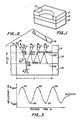
- a semiconductor structure that comprises a layer 11 of photoresist or other masking material that overlies and is contiguous to a second layer 13 of material that is to be etched wherever this second layer 13 is exposed and not covered by the masking material.
- the second layer 13 is assumed to overlie and be contiguous to a third layer 15, such as a semiconductor substrate, which differs from the material of the second layer 13 and is not to be etched. It is preferable that the particular region of the semiconductor structure illustrated in Fig. 1 is spaced apart from any portions of a circuit or other operating device that is part of the semiconductor structure, although it may also be provided proximate active devices of the semiconductor wafer.
- the aperture 17 may be formed by directing a laser beam of optical fluence typically > 0.1 Watts/cm2 of appropriate wavelength on the region of masking material laying within the area of the planned aperture 17, so that this cylinder of masking material is ablated (i.e. burned away), photochemically etched or otherwise removed from the first layer 11 in order to expose the upper surface of the second layer 13.
- the laser beam 22 spot activates an etchant gas to remove the material of layer 11 at aperture 17, while the surrounding layer 11 is substantially unaffected by the etchant gas.
- the laser wavelength ⁇ 2 may be chosen so that radiation of this wavelength is largely reflected by the second layer 13 of semiconductor material so that little or no material from this second layer 13 is removed in this aperture formation process.
- the laser wavelength ⁇ 2 may be chosen for high chemical selectivity so that radiation of wavelength ⁇ 2 induces or promotes ablation, chemical etching or other removal of the first layer 11 of material but does not do so for the second layer 13 of material. Other means of providing the aperture may also be used.
- An interrogating laser 29 (not shown in Fig. 1) or other source of highly monochromatic light 21 of wavelength ⁇ 1 of optical fluence ⁇ 0.2 Watt/cm2 is now directed through the aperture 17 at the exposed upper surface of the second layer 13 at a predetermined incidence angle ⁇ 1, as illustrated in Fig 2, and the reflected interferometric signal is monitored by a monitoring module 19 that is positioned to receive light beam rays that leave the upper surface of the layer 13 with a reflected angle of ⁇ 1. Formation of the aperture 17 should be done before the etching process begins, but monitoring of the reflected interferometric signal may begin before, at the time of, or after the etching process for the second layer 13 begins.
- the interrogating laser may also be used to monitor the remaining thickness of the masking material in the first layer 11 that is removed to form the aperture 17 therein. It is assumed here that the portion of the second layer 13 exposed by the aperture 17 will undergo etching at approximately the same rate at which etching of the exposed second layer 13 proceeds elsewhere.
- the diameter D of the aperture 17 is preferably sufficiently large that, at the chosen incidence angle ⁇ 1 for the light beam, the portion of the light beam that enters the second layer 13 of material undergoes several reflections at each of the interfaces between first and second layers and between second and third layers, and portions of these reflections emerge as refracted beams that leave the exposed surface of the second layer 13 within the aperture 17 at the angle of reflection ⁇ 1
- the upper surface of the layer 13 that is exposed by the aperture 17 is substantially planar, that the interface between the second layer 13 and the third layer 15 shown in Fig. 2 is substantially planar, and that these two planes are approximately parallel to one another.
- the wavelength ⁇ 1 of the interrogating laser is preferably chosen so that the material comprising the second layer 13 is at least partially transparent to light at the wavelength ⁇ 1.
- this approach may also be used where the second layer 13 is composed of a metal and other opaque material, such as aluminum.
- a light beam 21 of wavelength ⁇ 1 is incident on the exposed surface 13S of the second layer 13 within the aperture 17 at an incidence angle of ⁇ 1.
- a portion of this light beam 21 is reflected in a first component 21r at a reflection angle ⁇ 1, and a second component 21t of the light beam 21 is transmitted into the second layer 13 of material at a refracted angle ⁇ 2 in a well-known manner.
- a portion of the transmitted component 21t is transmitted into the third layer 15 of material and produces a component 21tt as shown; another portion is reflected as a reflected component 21tr, and a portion of this latter reflected component is transmitted at the first layer-second layer interface 13S to produce a component 21trt that moves away from this interface in a direction parallel to the original reflected component 21r.
- additional reflected components 21trrrt, 21trrrrrt, etc. are produced and move away from the interface 135 parallel to the original reflected component 21r.
- the angles ⁇ 1, ⁇ 2 and ⁇ 3 shown in Fig. 2 are related by Snell's law in a well-known manner.
- the set ⁇ h 2i,M ⁇ i of local maxima of layer thickness form a set of local extrema; and the set ⁇ h 2j,m ⁇ j of local minima of layer thickness for a separate set of local extrema.
- Two consecutive values of the thicknesses h 2i,M are spaced apart approximately by the distance where sec[x] denotes the secant of the angle x, and n1 and n2 are the refractive indices wavelength ⁇ 1 of the ambient medium, such as air or a very low pressure gas, and the second layer 13 of material, respectively.
- Two consecutive values of the thicknesses h 2j,m are spaced apart approximately by the same distance
- ⁇ h0 is the thickness of the second layer 13 that is removed or grown to reach the first thickness h 21,M or h 21,m in the maximum or minimum set of thicknesses, respectively.
- the end point of the growth process is determined by the desired thickness h2 of the layer to be grown.
- the etch process can be terminated or modified at any desired etch length H or at the end point, as desired.
- the average etch rate V k may be changed at a predetermined depth of the layer 13 in order to provide higher selectivity to the material in the layer 15 when the layer 15 is exposed.
- the reflectivity parameter R can be graphically displayed on the screen of a display module as a function of time so that the sequence of times at which R attains a local extremum value, a maximum or minimum, is easily identified from the display.
- the display module could also compute the average rate of change v of thickness of the second layer and display the numerical value of v and H, determined from Equations (3) and (4).
- an aperture 17 is first provided in the masking material as indicated in Fig. 1.
- a laser beam or other monochromatic light beam 21 of predetermined wavelength is then directed at a small portion of the upper surface of the first layer 13 of material that is exposed by the aperture 17, and a series of reflected images of the light beam are generated as indicated in Fig. 2.
- An interferometric monitoring module 19 is then positioned to receive these reflected images and to provide a graphical or numerical output indicating the present value of the reflectivity parameter R as a function of time.
- the increments ⁇ h2 of thickness of the first layer 13 that relate to two consecutive members of a maximum or minimum of thicknesses set, as illustrated in Fig. 3, is determined by the Equations (1) or (2).
- the average etch rate within a time interval defined by t i ⁇ t ⁇ t i+1 is given by Equation (3), and the total thickness of the second layer 13 consumed thus far is given by the Equation (4).
- the values of the reflectivity parameter R may be displayed graphically or numerically by the module 19.
- the laser fluence should be sufficiently high to allow easy ablation of the overlying masking material; fluences of at least 0.1 Watts/cm2 are typically used for general ablation.
- This laser beam may be produced by an excimer laser such as Ar, Xe or Kr; or the laser beam may be produced by a rare gas halide laser that utilizes a gas such as ArCl, XeCl, ArF, KrF or other similar compounds.
- Each of these lasers produces laser radiation in the ultraviolet or low visible region (wavelength ⁇ ⁇ 4000 ⁇ ).
- a laser that produces visible or near-infrared wavelengths, such as HeNe or a diode laser, may also be used here.
- the laser beam 21 used to form the aperture 17 could be delivered to the target spot on the masking material by a fiber optics cable or other means, as illustrated in Fig. 4.
- An excimer laser radiation source 23 produces an excimar laser beam of wavelength ⁇ 2 that is transported by one or more optical fibers 25 to a region adjacent to the intended aperture 17 in the first layer 13 of material; and focusing optics 27 focus and direct this laser beam to produce the aperture 17 in the first layer 13.
- a Q switch including material such as lithium niobate, may be provided adjacent to or within the excimer laser radiation source 23 to controllably release laser radiation onto the fiber 25.
- a laser radiation source 29 produces an interrogation radiation beam 21 of wavelength ⁇ 1, and this beam is directed into the aperture 17 produced by the excimer laser beam through a window 31 in a chamber 33 that contains the wafer being monitored.
- the chamber 33 may be provided with a gas outlet 35 to remove gas and produce a vacuum of selected level and with a gas inlet 37 to introduce a selected gas into the chamber 33.
- Additional optical fibers 26a, 26b, 26c may be used to transport the excimer laser radiation produced by the source 23 to other chambers.
- the laser beam of wavelength ⁇ 2 could be delivered to and focused on the target spot on the masking material by conventional mirrors and other optical components, In order to form the aperture 17 shown in Fig. 1, this laser beam or other light beam 21 may be pulsed at an appropriate rate such as 100-10,000 Hz.
- Masking materials for which an aperture can be formed therein include positive and negative photoresist, oxides of silicon, polysilicon, and layers of metal such as Al, Ag, Au, W and Ti and of silicides.
- This interferometry technique may also be used for measuring the rate of growth of or deposition on an exposed layer of semiconductor material. Further, the technique may be used to measure the changing thickness of any material, not restricted to semiconductor material, which is substantially transparent to light at some wavelength.
- the wavelength of the laser beam 22 can often be chosen so that the ablation or other aperture formation process is chemically selective and occurs only in the masking material, not in the underlying semiconductor material.
- Many masking materials are highly absorbent to electromagnetic radiation at ultraviolet wavelengths. If the underlying material has a "window" or limited range of ultraviolet wavelengths at which light absorption by the material is relatively small, use of a laser beam 22 with a wavelength in that limited range will promote selectivity. In this circumstance, the thickness detection apparatus would be turned off during aperture formation.
- a single light source might be used to provide the aperture 17 in the first layer 11 of material and to provide the monitoring beam for interferometrically measuring thickness change in the second layer 13. This may be accomplished by choosing a single wavelength ⁇ 3 that can serve both for aperture formation and for thickness monitoring. This may also be accomplished by providing a single light source whose radiative output can be switched between two different wavelengths ⁇ 1 and ⁇ 2.
- An example of a light source that is capable of alternatingly producing light 21, 22, of two different wavelengths is the dual frequency optical cavity disclosed by George et al. in U.S. Pat. No. 4,510,605, which is incorporated by reference herein.
- Other examples of apparatus that produces radiation of two or more wavelengths in an alternating manner are disclosed in U.S. Pat. No.
- a second layer 13 of material that is opaque or approximately 100 percent reflecting to the radiation of wavelength ⁇ 1 may also be used here.
- No substantial variation in interferometric signal R would be detected because all incident radiation either would be fully reflected at the first layer-second layer interface 135 or would be fully absorbed in the second layer 13.
- the reflectivity signal R from the interface 13S will change markedly at the end of an etch process, as the second layer 13 is fully consumed and the third layer 15 is exposed; and this change in reflected signal may be used to determine the end point of the etch process in the second layer.
- the radiation of wavelength ⁇ 2 may also be used to promote etching action or growth action at the exposed interface 13S of the second layer 13 by providing additional thermal energy, in the form of radiation photons delivered, sufficient to activate or maintain the etch or growth process.
- additional thermal energy in the form of radiation photons delivered, sufficient to activate or maintain the etch or growth process.
- Excimar lasers and rare gas halide lasers are available to produce and deliver photon energies up to at least 7.2 eV so that etching of most semiconductor and semiconductor oxide materials can be promoted using such lasers.
- the thickness detection apparatus may be used to monitor the thickness of the masking material as this material is ablated or otherwise by the laser beam 21, using another laser or light source with a visible or infrared wavelength to sense the changes in thickness in the remaining layer 11 of the ablating masking material by the technique disclosed above.
- the chemical composition of the ablated material can be analyzed spectroscopically or otherwise in real time as the ablation process proceeds; and when the ablation products that are characteristic of the masking material abruptly decrease in quantity, the ablation process is terminated and etching of the semiconductor layer or growth of a new layer may begin.
- Table 1 lists various masking materials and underlying layer materials for which the invention may be used to monitor the change in thickness of the underlying layer. Listing of particular materials in the Table is not intended to foreclose use of other materials. Table 1 Suitable Mask and Etch Layer Material Combinations.
- Masking Material Etch Layer Materials photoresist silicon, polysilicon, silicides, nitrides, oxynitrides, oxides, Al, Ti, Cu, W, Cr, TiN, TiW, GaAs, InP, PSG, BPSG oxide polysilicon, silicdes, nitrides, Al, Ti, Cu, W, Cr, TiN, TiW, GaAs, photoresist polysilicon oxides, PSG, BPSG Al oxides, PSG, BPSG, photoresist
Landscapes
- Physics & Mathematics (AREA)
- General Physics & Mathematics (AREA)
- Drying Of Semiconductors (AREA)
- Length Measuring Devices By Optical Means (AREA)
- ing And Chemical Polishing (AREA)
- Weting (AREA)
Applications Claiming Priority (2)
| Application Number | Priority Date | Filing Date | Title |
|---|---|---|---|
| US34819189A | 1989-05-05 | 1989-05-05 | |
| US348191 | 1989-05-05 |
Publications (2)
| Publication Number | Publication Date |
|---|---|
| EP0396010A2 true EP0396010A2 (fr) | 1990-11-07 |
| EP0396010A3 EP0396010A3 (fr) | 1991-03-27 |
Family
ID=23366971
Family Applications (1)
| Application Number | Title | Priority Date | Filing Date |
|---|---|---|---|
| EP19900107839 Withdrawn EP0396010A3 (fr) | 1989-05-05 | 1990-04-25 | Méthode et dispositif pour surveiller la vitesse de croissance et de décapage des matériaux |
Country Status (4)
| Country | Link |
|---|---|
| US (1) | US5465154A (fr) |
| EP (1) | EP0396010A3 (fr) |
| JP (1) | JP2516270B2 (fr) |
| KR (1) | KR900019187A (fr) |
Cited By (2)
| Publication number | Priority date | Publication date | Assignee | Title |
|---|---|---|---|---|
| EP0454604A3 (en) * | 1990-03-30 | 1992-10-21 | International Business Machines Corporation | Laser ablation for plasma etching endpoint detection |
| WO1993006480A1 (fr) * | 1991-09-17 | 1993-04-01 | Exxon Research And Engineering Company | Detecteur de fluorure d'hydrogene |
Families Citing this family (49)
| Publication number | Priority date | Publication date | Assignee | Title |
|---|---|---|---|---|
| JP2612089B2 (ja) * | 1990-08-10 | 1997-05-21 | 富士通株式会社 | 被エッチング膜の膜厚検出方法、膜厚検出装置及びエッチング装置 |
| JP2653017B2 (ja) * | 1993-08-10 | 1997-09-10 | 日本電気株式会社 | ドライエッチング深さ測定方法および装置 |
| JP3491337B2 (ja) * | 1994-05-13 | 2004-01-26 | 株式会社デンソー | 半導体厚非接触測定装置 |
| DE69510032T2 (de) * | 1995-03-31 | 2000-01-27 | International Business Machines Corp., Armonk | Verfahren und Gerät zur Überwachung des Trockenätzens eines dielektrischen Films bis zu einer gegebenen Dicke |
| US5591300A (en) * | 1995-06-07 | 1997-01-07 | Vtc Inc. | Single crystal silicon dry-etch endpoint based on dopant-dependent and thermally-assisted etch rates |
| US5960107A (en) * | 1995-12-28 | 1999-09-28 | Vlsi Technology, Inc. | Method for verifying an average topography height function of a photostepper |
| US5777739A (en) * | 1996-02-16 | 1998-07-07 | Micron Technology, Inc. | Endpoint detector and method for measuring a change in wafer thickness in chemical-mechanical polishing of semiconductor wafers |
| US6075606A (en) | 1996-02-16 | 2000-06-13 | Doan; Trung T. | Endpoint detector and method for measuring a change in wafer thickness in chemical-mechanical polishing of semiconductor wafers and other microelectronic substrates |
| US5998305A (en) * | 1996-03-29 | 1999-12-07 | Praxair Technology, Inc. | Removal of carbon from substrate surfaces |
| US5739906A (en) * | 1996-06-07 | 1998-04-14 | The United States Of America As Represented By The Secretary Of Commerce | Interferometric thickness variation test method for windows and silicon wafers using a diverging wavefront |
| US5940175A (en) * | 1996-11-01 | 1999-08-17 | Msp Corporation | Method and apparatus for surface inspection in a chamber |
| US5712702A (en) * | 1996-12-06 | 1998-01-27 | International Business Machines Corporation | Method and apparatus for determining chamber cleaning end point |
| US5694207A (en) * | 1996-12-09 | 1997-12-02 | Taiwan Semiconductor Manufacturing Company, Ltd. | Etch rate monitoring by optical emission spectroscopy |
| US6025916A (en) * | 1997-02-27 | 2000-02-15 | Wisconsin Alumni Research Foundation | Wall deposition thickness sensor for plasma processing chamber |
| US6090102A (en) * | 1997-05-12 | 2000-07-18 | Irvision, Inc. | Short pulse mid-infrared laser source for surgery |
| US6007408A (en) * | 1997-08-21 | 1999-12-28 | Micron Technology, Inc. | Method and apparatus for endpointing mechanical and chemical-mechanical polishing of substrates |
| US6632321B2 (en) | 1998-01-06 | 2003-10-14 | Applied Materials, Inc | Method and apparatus for monitoring and controlling wafer fabrication process |
| US6020957A (en) * | 1998-04-30 | 2000-02-01 | Kla-Tencor Corporation | System and method for inspecting semiconductor wafers |
| US6075909A (en) * | 1998-06-26 | 2000-06-13 | Lucent Technologies, Inc. | Optical monitoring system for III-V wafer processing |
| US6046111A (en) * | 1998-09-02 | 2000-04-04 | Micron Technology, Inc. | Method and apparatus for endpointing mechanical and chemical-mechanical planarization of microelectronic substrates |
| US6228277B1 (en) * | 1998-10-14 | 2001-05-08 | Lucent Technologies Inc. | Etch endpoint detection |
| US6124927A (en) * | 1999-05-19 | 2000-09-26 | Chartered Semiconductor Manufacturing Ltd. | Method to protect chamber wall from etching by endpoint plasma clean |
| US6160621A (en) * | 1999-09-30 | 2000-12-12 | Lam Research Corporation | Method and apparatus for in-situ monitoring of plasma etch and deposition processes using a pulsed broadband light source |
| US6642150B1 (en) | 1999-12-28 | 2003-11-04 | Taiwan Semiconductor Manufacturing Company | Method for testing for blind hole formed in wafer layer |
| US6785011B1 (en) | 2000-03-16 | 2004-08-31 | Lexmark International, Inc | Optical sensor arrangement for start of scan detection and improved vertical beam alignment range |
| US6290572B1 (en) | 2000-03-23 | 2001-09-18 | Micron Technology, Inc. | Devices and methods for in-situ control of mechanical or chemical-mechanical planarization of microelectronic-device substrate assemblies |
| US6612901B1 (en) | 2000-06-07 | 2003-09-02 | Micron Technology, Inc. | Apparatus for in-situ optical endpointing of web-format planarizing machines in mechanical or chemical-mechanical planarization of microelectronic-device substrate assemblies |
| US6428386B1 (en) | 2000-06-16 | 2002-08-06 | Micron Technology, Inc. | Planarizing pads, planarizing machines, and methods for mechanical and/or chemical-mechanical planarization of microelectronic-device substrate assemblies |
| US6609947B1 (en) | 2000-08-30 | 2003-08-26 | Micron Technology, Inc. | Planarizing machines and control systems for mechanical and/or chemical-mechanical planarization of micro electronic substrates |
| US6447369B1 (en) | 2000-08-30 | 2002-09-10 | Micron Technology, Inc. | Planarizing machines and alignment systems for mechanical and/or chemical-mechanical planarization of microelectronic substrates |
| JP2002246430A (ja) * | 2001-02-21 | 2002-08-30 | Hitachi Ltd | 半導体装置の製造方法 |
| JP2002278473A (ja) * | 2001-03-21 | 2002-09-27 | Sony Corp | 表示パネルの製造方法 |
| KR20020086760A (ko) * | 2001-05-10 | 2002-11-20 | 동부전자 주식회사 | 측정 조사용 기준 웨이퍼와 이를 이용한 장비의 측정 조사방법 |
| US6697094B2 (en) | 2001-05-14 | 2004-02-24 | Lexmark International, Inc. | Method and apparatus for locating the process postion of a scan line in an electrophotographic machine |
| US7196800B1 (en) * | 2001-07-26 | 2007-03-27 | Advanced Micro Devices, Inc. | Semiconductor die analysis as a function of optical reflections from the die |
| US7253901B2 (en) | 2002-01-23 | 2007-08-07 | Kla-Tencor Technologies Corporation | Laser-based cleaning device for film analysis tool |
| US7341502B2 (en) | 2002-07-18 | 2008-03-11 | Micron Technology, Inc. | Methods and systems for planarizing workpieces, e.g., microelectronic workpieces |
| KR100699859B1 (ko) | 2005-08-11 | 2007-03-27 | 삼성전자주식회사 | 반도체 설비의 캘리브레이션용 기준 웨이퍼 |
| JP2008218956A (ja) * | 2007-03-08 | 2008-09-18 | Sharp Corp | 半導体レーザ素子の製造方法および半導体レーザ素子 |
| JP5396703B2 (ja) * | 2007-10-09 | 2014-01-22 | 富士通セミコンダクター株式会社 | 熱処理装置及び方法、並びに半導体装置の製造方法 |
| US10189100B2 (en) * | 2008-07-29 | 2019-01-29 | Pratt & Whitney Canada Corp. | Method for wire electro-discharge machining a part |
| US8925201B2 (en) * | 2009-06-29 | 2015-01-06 | Pratt & Whitney Canada Corp. | Method and apparatus for providing rotor discs |
| US10340128B2 (en) * | 2015-07-16 | 2019-07-02 | Toshiba Memory Corporation | Apparatus, method and nontransitory computer readable medium for manufacturing integrated circuit device |
| US10340170B2 (en) * | 2016-02-12 | 2019-07-02 | Asm Technology Singapore Pte Ltd | Method and device for grooving wafers |
| DE102017204861A1 (de) * | 2017-03-23 | 2018-09-27 | Carl Zeiss Smt Gmbh | Verfahren zum Bestimmen eines Materialabtrags und Vorrichtung zur Strahlbearbeitung eines Werkstücks |
| US10852125B2 (en) | 2017-11-28 | 2020-12-01 | Koh Young Technology Inc. | Apparatus for inspecting film on substrate by using optical interference and method thereof |
| KR102195240B1 (ko) * | 2017-11-28 | 2020-12-24 | 주식회사 고영테크놀러지 | 기판 검사 장치 및 기판 검사 방법 |
| US10859371B2 (en) | 2017-11-28 | 2020-12-08 | Koh Young Technology Inc. | Apparatus for inspecting substrate and method thereof |
| CN111063627A (zh) * | 2019-12-30 | 2020-04-24 | 中电国基南方集团有限公司 | Bcb厚度的在片监测与控制方法及装置 |
Family Cites Families (17)
| Publication number | Priority date | Publication date | Assignee | Title |
|---|---|---|---|---|
| DE1097148B (de) * | 1955-06-23 | 1961-01-12 | Philco Corp | Verfahren und Vorrichtung zur Dickenkontrolle von Halbleiterkoerpern bei der Bearbeitung |
| US3299275A (en) * | 1963-08-14 | 1967-01-17 | Boeing Co | Measuring surface temperatures of ablating materials with thermocouple and photocell |
| US3518133A (en) * | 1967-06-01 | 1970-06-30 | Us Army | Method for measuring the thickness of a diffused surface layer |
| US4367044A (en) * | 1980-12-31 | 1983-01-04 | International Business Machines Corp. | Situ rate and depth monitor for silicon etching |
| JPS5886787A (ja) * | 1981-11-19 | 1983-05-24 | Nippon Sekigaisen Kogyo Kk | レ−ザ照射装置 |
| US4510605A (en) * | 1983-03-21 | 1985-04-09 | The United States Of America As Represented By The United States Department Of Energy | Dual frequency optical cavity |
| CA1251846A (fr) * | 1983-09-26 | 1989-03-28 | Masataka Shirasaki | Source de lumiere laser |
| US4618262A (en) * | 1984-04-13 | 1986-10-21 | Applied Materials, Inc. | Laser interferometer system and method for monitoring and controlling IC processing |
| US4660979A (en) * | 1984-08-17 | 1987-04-28 | At&T Technologies, Inc. | Method and apparatus for automatically measuring semiconductor etching process parameters |
| US4680084A (en) * | 1984-08-21 | 1987-07-14 | American Telephone And Telegraph Company, At&T Bell Laboratories | Interferometric methods and apparatus for device fabrication |
| US4747110A (en) * | 1985-02-13 | 1988-05-24 | Matsushita Electric Industrial Co., Ltd. | Semiconductor laser device capable of emitting laser beams of different wavelengths |
| US4660205A (en) * | 1985-05-13 | 1987-04-21 | Allied Corporation | Multi-resonator switching laser |
| JPS63140940A (ja) * | 1986-12-02 | 1988-06-13 | Ricoh Co Ltd | 屈折率・膜厚測定方法 |
| JPS63147327A (ja) * | 1986-12-10 | 1988-06-20 | Dainippon Screen Mfg Co Ltd | 表面処理における処理終点検知方法 |
| US4751706A (en) * | 1986-12-31 | 1988-06-14 | The United States Of America As Represented By The Secretary Of The Army | Laser for providing rapid sequence of different wavelengths |
| GB2203892A (en) * | 1987-04-24 | 1988-10-26 | Philips Electronic Associated | A method of etching a semiconductor body |
| US4975141A (en) * | 1990-03-30 | 1990-12-04 | International Business Machines Corporation | Laser ablation for plasma etching endpoint detection |
-
1990
- 1990-04-25 EP EP19900107839 patent/EP0396010A3/fr not_active Withdrawn
- 1990-05-07 KR KR1019900006539A patent/KR900019187A/ko not_active Withdrawn
- 1990-05-07 JP JP2117334A patent/JP2516270B2/ja not_active Expired - Lifetime
- 1990-12-21 US US07/632,413 patent/US5465154A/en not_active Expired - Lifetime
Cited By (2)
| Publication number | Priority date | Publication date | Assignee | Title |
|---|---|---|---|---|
| EP0454604A3 (en) * | 1990-03-30 | 1992-10-21 | International Business Machines Corporation | Laser ablation for plasma etching endpoint detection |
| WO1993006480A1 (fr) * | 1991-09-17 | 1993-04-01 | Exxon Research And Engineering Company | Detecteur de fluorure d'hydrogene |
Also Published As
| Publication number | Publication date |
|---|---|
| JPH02307003A (ja) | 1990-12-20 |
| JP2516270B2 (ja) | 1996-07-24 |
| EP0396010A3 (fr) | 1991-03-27 |
| KR900019187A (ko) | 1990-12-24 |
| US5465154A (en) | 1995-11-07 |
Similar Documents
| Publication | Publication Date | Title |
|---|---|---|
| EP0396010A2 (fr) | Méthode et dispositif pour surveiller la vitesse de croissance et de décapage des matériaux | |
| US4618262A (en) | Laser interferometer system and method for monitoring and controlling IC processing | |
| EP1296367B1 (fr) | Dispositif et procede de mesure d'epaisseur, dispositif et procede de gravure humide utilisant les precedents | |
| USRE39145E1 (en) | Method and apparatus for in-situ monitoring of plasma etch and deposition processes using a pulsed broadband light source | |
| US6100985A (en) | Method and apparatus for measurements of patterned structures | |
| US6897964B2 (en) | Thickness measuring apparatus, thickness measuring method, and wet etching apparatus and wet etching method utilizing them | |
| US6476920B1 (en) | Method and apparatus for measurements of patterned structures | |
| JPH0834199B2 (ja) | エッチング終点検出方法及び装置 | |
| JP2000326221A (ja) | 研磨監視方法、研磨方法及び研磨装置 | |
| JPH1133901A (ja) | ウェハ研磨装置 | |
| US6836324B2 (en) | Method and apparatus for measurements of patterned structures | |
| JP4427767B2 (ja) | 測定方法 | |
| KR100893961B1 (ko) | 실시간 에칭율을 결정하기 위한 섈로우-앵글 간섭 공정 및장치 | |
| EP1037012B1 (fr) | Procédé et dispositif pour mesurer des structures à dessins | |
| US20050117165A1 (en) | Semiconductor etching process control | |
| EP0412728A2 (fr) | Méthode et dispositif interférométrique pour contrôler l'épaisseur d'un film | |
| EP0462599B1 (fr) | Appareil et méthode pour mesurer la vitesse de décapage | |
| US20030082838A1 (en) | Method and system for monitoring a semiconductor wafer plasma etch process | |
| WO2003092049A1 (fr) | Amelioration relative au controle des processus dans les processus de gravure | |
| JPH08201279A (ja) | スペクトル測定装置 | |
| JP2001260016A (ja) | 研磨状態測定装置及び測定方法及び研磨装置及び半導体デバイス製造方法 | |
| KR20010010469A (ko) | 기판 식각 장치 및 이를 이용한 실리콘 맴브레인 제조 방법 | |
| JPH02108905A (ja) | 現場フィルム成長計測の為の二つのレーザ干渉計 | |
| JPS62271434A (ja) | エツチング完了点検出方法 |
Legal Events
| Date | Code | Title | Description |
|---|---|---|---|
| PUAI | Public reference made under article 153(3) epc to a published international application that has entered the european phase |
Free format text: ORIGINAL CODE: 0009012 |
|
| AK | Designated contracting states |
Kind code of ref document: A2 Designated state(s): BE DE ES FR GB IT NL |
|
| PUAL | Search report despatched |
Free format text: ORIGINAL CODE: 0009013 |
|
| AK | Designated contracting states |
Kind code of ref document: A3 Designated state(s): BE DE ES FR GB IT NL |
|
| 17P | Request for examination filed |
Effective date: 19910614 |
|
| 17Q | First examination report despatched |
Effective date: 19930301 |
|
| STAA | Information on the status of an ep patent application or granted ep patent |
Free format text: STATUS: THE APPLICATION IS DEEMED TO BE WITHDRAWN |
|
| 18D | Application deemed to be withdrawn |
Effective date: 19930713 |