EP1296367B1 - Dispositif et procede de mesure d'epaisseur, dispositif et procede de gravure humide utilisant les precedents - Google Patents
Dispositif et procede de mesure d'epaisseur, dispositif et procede de gravure humide utilisant les precedents Download PDFInfo
- Publication number
- EP1296367B1 EP1296367B1 EP01901468A EP01901468A EP1296367B1 EP 1296367 B1 EP1296367 B1 EP 1296367B1 EP 01901468 A EP01901468 A EP 01901468A EP 01901468 A EP01901468 A EP 01901468A EP 1296367 B1 EP1296367 B1 EP 1296367B1
- Authority
- EP
- European Patent Office
- Prior art keywords
- thickness
- light
- measurement
- time
- raw
- Prior art date
- Legal status (The legal status is an assumption and is not a legal conclusion. Google has not performed a legal analysis and makes no representation as to the accuracy of the status listed.)
- Expired - Lifetime
Links
Images



Classifications
-
- G—PHYSICS
- G01—MEASURING; TESTING
- G01B—MEASURING LENGTH, THICKNESS OR SIMILAR LINEAR DIMENSIONS; MEASURING ANGLES; MEASURING AREAS; MEASURING IRREGULARITIES OF SURFACES OR CONTOURS
- G01B11/00—Measuring arrangements characterised by the use of optical techniques
- G01B11/02—Measuring arrangements characterised by the use of optical techniques for measuring length, width or thickness
- G01B11/06—Measuring arrangements characterised by the use of optical techniques for measuring length, width or thickness for measuring thickness ; e.g. of sheet material
- G01B11/0616—Measuring arrangements characterised by the use of optical techniques for measuring length, width or thickness for measuring thickness ; e.g. of sheet material of coating
- G01B11/0683—Measuring arrangements characterised by the use of optical techniques for measuring length, width or thickness for measuring thickness ; e.g. of sheet material of coating measurement during deposition or removal of the layer
-
- G—PHYSICS
- G01—MEASURING; TESTING
- G01B—MEASURING LENGTH, THICKNESS OR SIMILAR LINEAR DIMENSIONS; MEASURING ANGLES; MEASURING AREAS; MEASURING IRREGULARITIES OF SURFACES OR CONTOURS
- G01B11/00—Measuring arrangements characterised by the use of optical techniques
- G01B11/02—Measuring arrangements characterised by the use of optical techniques for measuring length, width or thickness
- G01B11/06—Measuring arrangements characterised by the use of optical techniques for measuring length, width or thickness for measuring thickness ; e.g. of sheet material
- G01B11/0616—Measuring arrangements characterised by the use of optical techniques for measuring length, width or thickness for measuring thickness ; e.g. of sheet material of coating
- G01B11/0675—Measuring arrangements characterised by the use of optical techniques for measuring length, width or thickness for measuring thickness ; e.g. of sheet material of coating using interferometry
-
- H—ELECTRICITY
- H10—SEMICONDUCTOR DEVICES; ELECTRIC SOLID-STATE DEVICES NOT OTHERWISE PROVIDED FOR
- H10P—GENERIC PROCESSES OR APPARATUS FOR THE MANUFACTURE OR TREATMENT OF DEVICES COVERED BY CLASS H10
- H10P72/00—Handling or holding of wafers, substrates or devices during manufacture or treatment thereof
- H10P72/06—Apparatus for monitoring, sorting, marking, testing or measuring
- H10P72/0604—Process monitoring, e.g. flow or thickness monitoring
-
- H—ELECTRICITY
- H10—SEMICONDUCTOR DEVICES; ELECTRIC SOLID-STATE DEVICES NOT OTHERWISE PROVIDED FOR
- H10P—GENERIC PROCESSES OR APPARATUS FOR THE MANUFACTURE OR TREATMENT OF DEVICES COVERED BY CLASS H10
- H10P74/00—Testing or measuring during manufacture or treatment of wafers, substrates or devices
- H10P74/20—Testing or measuring during manufacture or treatment of wafers, substrates or devices characterised by the properties tested or measured, e.g. structural or electrical properties
- H10P74/203—Structural properties, e.g. testing or measuring thicknesses, line widths, warpage, bond strengths or physical defects
Definitions
- the present invention relates to a thickness measuring apparatus and thickness measuring method of measuring the thickness of a semiconductor wafer during execution of wet etching and a wet etching apparatus and wet etching method using the thickness measuring apparatus and method.
- a wet etching apparatus for etching a semiconductor wafer while supplying an etchant is used.
- a dummy wafer is etched to confirm the etching rate in advance, and the etching end time is determined on the basis of the etching rate.
- the thickness of a semiconductor wafer portion must be measured in situ during etching. With this measurement, data of a change in thickness over time during etching can be obtained whereby the end time can be obtained for each etching process. That is, various etching processes can be managed and controlled.
- Conventional semiconductor wafer thickness measuring apparatuses include a contact thickness meter and Michelson interference thickness meter. Of these thickness meters, the contact thickness meter cannot be applied to measurement in situ. In addition, since this thickness meter comes into contact with a semiconductor wafer, the wafer may be damaged, and therefore, measurement at a high speed is impossible. If a wafer has a holding substrate or film, the thickness of only the wafer cannot be measured.
- the Michelson interference thickness meter measures the thickness of a semiconductor wafer in a noncontact state.
- a thickness meter an apparatus is disclosed in Japanese Patent Application Laid-Open No. H5-248817. This apparatus irradiates a semiconductor wafer with measurement light and measures a change in thickness over time on the basis of a change in reflection timing of reflected light from the wafer surface. In this case, however, only the position on the upper surface is measured. To obtain the thickness, an initial condition of thickness, such as the position on the lower surface, must be given. Additionally, in a wet etching process using an etchant, since measurement light is reflected by the etchant on the wafer surface, the thickness of the semiconductor wafer cannot be measured.
- the present invention has been made to solve the above problems, and has as its object to provide a thickness measuring apparatus and thickness measuring method which can measure the thickness of a semiconductor wafer during execution of wet etching, and a wet etching apparatus and wet etching method using the thickness measuring apparatus and method.
- a thickness measuring apparatus for measuring a thickness of a semiconductor wafer during execution of wet etching using an etchant, characterized by comprising (1) a measurement light source which supplies measurement light at each of a plurality of measurement times at a predetermined time interval, (2) light branching means for branching the measurement light from the measurement light source, (3) light output means for outputting one component of the measurement light branched by the light branching means to the semiconductor wafer as a measurement object so as to irradiate the semiconductor wafer from a side of an etching surface to which the etchant is being supplied, (4) light input means for inputting reflected light obtained when the measurement light irradiated from the light output means is reflected by the etchant or semiconductor wafer, (5) reference light generating means for passing the other component of the measurement light branched by the light branching means through a reference optical path designed to be able to change an optical path length so as to generate reference light for which a
- a thickness measuring method of measuring a thickness of a semiconductor wafer during execution of wet etching using an etchant characterized by comprising (1) the measurement light supply step of supplying measurement light from a measurement light source at each of a plurality of measurement times at a predetermined time interval, (2) the light branching step of branching the measurement light from the measurement light source, (3) the light output step of outputting one component of the measurement light branched in the light branching step to the semiconductor wafer as a measurement object so as to irradiate the semiconductor wafer from a side of an etching surface to which the etchant is being supplied, (4) the light input step of inputting reflected light obtained when the measurement light irradiated in the light output step is reflected by the etchant or semiconductor wafer, (5) the reference light generating step of passing the other component of the measurement light branched in the light branching step through a reference optical path designed to be able to change an optical path length so as to generate reference light for
- reflected light obtained when the semiconductor wafer is irradiated with measurement light, and the measurement light is reflected is coupled to reference light that is branched from the measurement light and passes through a predetermined optical path to set a reference optical path length with respect to the optical path length of the reflected light, and the resultant interference light is detected.
- the thickness of the semiconductor wafer during wet etching is measured from a plurality of light intensity peaks generated in the light intensity distribution of the interference light.
- the measurement light with which the semiconductor wafer is irradiated is reflected by the etchant surface and the upper surface (etching surface) and lower surface of the semiconductor wafer.
- Light intensity peaks corresponding to the surfaces are obtained in the light intensity distribution.
- the thickness of the semiconductor wafer or a time-rate change in thickness can be measured during wet etching independently of the presence of the etchant.
- reflected light from both the upper and lower surfaces of the wafer is used. For this reason, even when the state of the semiconductor wafer or etchant changes, the thickness of the semiconductor wafer can always be accurately measured.
- the raw thickness value sorted by statistical processing at the first measurement time after the elapse of the specified time and the determined thickness change line are initial conditions of statistical processing at each of the second and subsequent measurement times.
- the end of wet etching by stopping supply of the etchant, or change of the etching rate can be appropriately controlled through the etching control means.
- Fig. 1 is a block diagram showing an embodiment of a thickness measuring apparatus and a wet etching apparatus having the thickness measuring apparatus.
- This wet etching apparatus comprises a thickness measuring apparatus A and a normal wet etching apparatus B except for the thickness measuring apparatus A (this apparatus portion will be simply referred to as a wet etching apparatus B hereinafter).
- the thickness measuring apparatus A is a noncontact thickness meter designed to irradiate a semiconductor wafer W to be measured with measurement light and measure the thickness of the semiconductor wafer W using a change in light intensity of interference light between reference light and reflected light from the semiconductor wafer W.
- Measurement light to be used for thickness measurement is supplied from a measurement light source 11 at each of a plurality of measurement times at a predetermined time interval (measurement light supply step).
- the measurement light output from the measurement light source 11 is input to an optical coupler 12 formed from a fiber coupler through an input optical fiber 11a.
- a low-coherence light source e.g., an SLD that generates light having a wavelength of 1.3 ⁇ m
- the wavelength of measurement light a wavelength that is sufficiently transmitted through the semiconductor wafer W or an etchant is selected.
- the optical coupler 12 functions as a light branching means for branching the measurement light from the measurement light source 11.
- the measurement light input to the optical coupler 12 is branched to a measurement optical fiber 13a leading to a measurement optical path and a reference optical fiber 14a leading to a reference optical path (light branching step).
- the branched measurement light components are input to a probe head 13 for measuring the thickness and a reference light generating section 14 for generating reference light, respectively.
- the probe head 13 is a light input/output means functioning as a light output means for irradiating the semiconductor wafer W with measurement light and a light input means for inputting again reflected light that is generated when the semiconductor wafer W or an etchant reflects the measurement light.
- the measurement light branched to the optical fiber 13a side is output from the probe head 13 to the semiconductor wafer W.
- the semiconductor wafer W is irradiated with the measurement light from the etching surface on the upper side (light output step).
- As this measurement light light having a wavelength that is sufficiently transmitted through the semiconductor wafer W or the like is used, as described above.
- Some components of the measurement light are reflected by each interface.
- the reflected light reaches and is input to the probe head 13 again (light input step).
- the reflected light that reaches and is re-input to the probe head 13 is input to the optical coupler 12 through the optical fiber 13a.
- reference light used to measure the thickness (optical path length) as interference light with reflected light from the semiconductor wafer W or the like is generated (reference light generation step).
- the measurement light branched to the optical fiber 14a side by the optical coupler 12 changes to reference light for which the optical path length of reference light (reference optical path length) with respect to the optical path length of reflected light (reflection optical path length) from the semiconductor wafer W or the like is set through a reference optical path 14b formed from an optical path length modulation optical system arranged between the output terminal of the optical fiber 14a and a reflecting mirror 14c.
- the measurement light output from the output terminal of the optical fiber 14a is transmitted through a parallel-plate glass substrate 14d and reaches and is reflected by the reflecting mirror 14c. Reflected light from the reflecting mirror 14c is transmitted through the glass substrate 14d again in the reverse direction and is input to the optical coupler 12 through the optical fiber 14a as reference light for which an appropriate reference optical path length is set.
- the reference light generating section 14 is designed to change the optical path length of the reference optical path 14b. More specifically, the glass substrate 14d on the reference optical path 14b is attached to a galvanometer 14e.
- the galvanometer 14e operates on the basis of a periodical signal from a reference optical path length control section 17 whereby the tilt of the glass substrate 14d with respect to the reference optical path 14b periodically changes. At this time, the thickness of the glass substrate 14d when viewed from the direction of reference optical path 14b changes.
- the optical path length of the reference optical path 14b periodically changes, and the reference optical path length with respect to the reflection optical path length (timing of reference light with respect to reflected light) is periodically scanned.
- the optical coupler 12 serves as a light branching means for branching the measurement light from the measurement light source 11 and also functions as a light coupling means for coupling the reflected light from the probe head 13 to the reference light from the reference light generating section 14.
- the reflected light that is reflected by the semiconductor wafer W or the like and returns and is input to the probe head 13, and the reference light for which the reference optical path length is set in the reference light generating section 14 are coupled by the optical coupler 12 into interference light (light coupling step).
- the interference light is input to a photodetector 15 such as a photodiode (PD) through an output optical fiber 15a and detected (photodetection step).
- the data and the like of the interference light detected by the photodetector 15 are processed by a thickness calculating section 16.
- the thickness of the semiconductor wafer W is calculated (thickness calculation step).
- a detection signal obtained by detecting interference light by the photodetector 15 is input to a raw thickness value calculating section 16b through a signal processing circuit 16a in the thickness calculating section 16.
- the data of light intensity of the interference light is obtained by the detection signal from the photodetector 15.
- the angle signal of the galvanometer 14e (glass substrate 14d) from the reference optical path length control section 17 is also input to the raw thickness value calculating section 16b through the signal processing circuit 16a.
- the data of the reference optical path length or its optical path length change amount in the reference optical path 14b is obtained from the angle signal.
- a light intensity distribution representing a change (correlation) in light intensity of interference light by the reference optical path length is generated from the light intensity data and reference optical path length data.
- a plurality of light intensity peaks are specified as peaks having peak intensities that exceed a threshold intensity.
- the raw thickness value of the semiconductor wafer W is calculated using two light intensity peaks selected from these light intensity peaks (raw thickness value calculation step).
- the raw thickness value calculated by the raw thickness value calculating section 16b is further input to a statistical thickness value calculating section 16c.
- a thickness change line is determined by linear approximation for a time-rate change in a plurality of raw thickness values, and a statistical thickness value is calculated (statistical thickness value calculation step).
- the wet etching apparatus B is designed to wet-etch one surface (the upper surface in Fig. 1; to be referred to as an etching surface hereinafter) of the semiconductor wafer W as an etching process object (a measurement object of the thickness measuring apparatus A) using an etchant.
- the semiconductor wafer W is fixed on a rotary table 22 while being held by a holding substrate 21 formed from a glass substrate arranged on the opposite surface side of the etching surface.
- the rotary table 22 is rotatably driven by a rotational driving section 23, thereby rotating the semiconductor wafer W during wet etching.
- the semiconductor wafer W has a pattern
- the surface with the pattern is set on the holding substrate 21 side. Wet etching is performed while setting the surface on the opposite side of the pattern as the etching surface.
- Etchant supply to the etching surface of the semiconductor wafer W is done by an etchant supply section 24.
- the etchant supply section 24 supplies or stops an etchant or supplies cleaning water to the semiconductor wafer W.
- an etchant is supplied from a nozzle 24a to the etching surface of the rotating semiconductor wafer W by the etchant supply section 24, the supplied etchant forms a thin etchant layer E on the surface of the semiconductor wafer W.
- the surface of the semiconductor wafer W is wet-etched by the etchant layer E.
- Rotation of the rotary table 22, the holding substrate 21 mounted on the rotary table 22, and the semiconductor wafer W by the rotational driving section 23 and supply/stop of an etchant or cleaning water to the etching surface of the semiconductor wafer W by the etchant supply section 24 are controlled by an etching control section 25.
- the probe head 13 of the thickness measuring apparatus A is set at a position opposing a predetermined portion of the etching surface of the semiconductor wafer W placed on the rotary table 22 together with the holding substrate 21 such that the optical path of measurement light with which the etching surface is irradiated becomes almost perpendicular to the etching surface. At this time, reflected light that is generated when the measurement light with which the etching surface is perpendicularly irradiated is reflected by the semiconductor wafer W or the like is efficiently re-input to the probe head 13.
- the probe head 13 preferably has, as a protective film, a transparent sheet made of, e.g., polyvinyl chloride that is resistant against the etchant.
- a transparent sheet made of, e.g., polyvinyl chloride that is resistant against the etchant.
- sticking of the etchant may be prevented by attaching a cylinder to the distal end of the probe head 13 and pressurizing the interior of the cylinder.
- a wet etching method for the semiconductor wafer W using the wet etching apparatus shown in Fig. 1, which is formed from the thickness measuring apparatus A and wet etching apparatus B, will be described using an example.
- the semiconductor wafer W held by the holding substrate 21 is placed on the rotary table 22.
- Rotational driving of the rotary table 22 is started on the basis of an instruction signal from the etching control section 25.
- the etchant supply section 24 is instructed to supply an etchant to the etching surface of the semiconductor wafer W, and wet etching of the semiconductor wafer W is started (etching start step).
- the thickness of the semiconductor wafer W is measured by the above-described thickness measuring apparatus A and thickness measuring method (thickness measurement step). Thickness measurement is executed at a measurement time instructed by the operator or automatically executed at measurement times at a preset time interval.
- the raw thickness value calculating section 16b calculates the raw thickness value from thickness data acquired at each measurement time.
- the statistical thickness value calculating section 16c calculates a thickness change line representing a change in thickness over time and a statistical thickness value obtained by statistical processing by using the raw thickness values acquired at measurement times.
- the thickness of the semiconductor wafer W in the wet etching process in progress and the change in thickness over time are evaluated from the thickness change line and statistical thickness value. Thickness evaluation can be automatically done by, e.g., the thickness calculating section 16 of the thickness measuring apparatus A. Alternatively, a display device may be connected to the thickness calculating section 16 to display the thickness data on the display device and cause the operator to do evaluation on the basis of the displayed data.
- the wet etching end time may be determined on the basis of etching time or etching rate data given in advance.
- the end time at which a set terminal thickness is obtained is preferably calculated from a thickness change line obtained for the data of raw thickness values measured by the thickness measuring apparatus A (end time calculation step).
- the end time may be automatically obtained by the statistical thickness value calculating section 16c or determined by the operator from data displayed on the display device.
- an end instruction signal for instructing the end time may be output from the statistical thickness value calculating section 16c of the thickness calculating section 16, and the etching control section 25 may control the end of wet etching on the basis of the end instruction signal.
- Figs. 2A and 2B are views schematically showing the method of measuring the thickness of the semiconductor wafer W in the wet etching apparatus shown in Fig. 1.
- Fig. 2A is a side sectional view showing irradiation of the semiconductor wafer W with measurement light and re-input of reflected light to the probe head 13.
- Fig. 2B is a graph showing the light intensity distribution of interference light obtained by the photodetector 15. Referring to Fig. 2A, the position of the optical path of measurement light with which the semiconductor wafer W is irradiated is shifted from the position of the optical path of reflected light to the probe head 13, for the illustrative convenience.
- Measurement light L0 branched by the optical coupler 12 and output from the probe head 13 is sequentially transmitted through the etchant layer E, semiconductor wafer W, and holding substrate 21. Some components of the measurement light L0 are reflected by the interfaces between adjacent layers. More specifically, reflected light L1 returns from the surface of the etchant layer E, reflected light L2 returns from the upper surface of the semiconductor wafer W, reflected light L3 returns from the lower surface of the semiconductor wafer W, and reflected light L4 returns from the lower surface of the holding substrate 21. These reflected light components return to and are re-input to the probe head 13.
- the re-input reflected light components L1 to L4 pass through different reflection optical path lengths depending on the interfaces that reflect them, as shown in Fig. 2A, so the reflected light components are input from the probe head 13 to the photodetector 15 through the optical coupler 12 at different timings.
- the optical path length of the reference optical path 14b is periodically changed, as described above, and the reference optical path length (timing of reference light with respect to reflected light) is scanned.
- Fig. 2B shows a light intensity distribution representing the correlation between the interference light intensity and the reference optical path length (optical path length change amount) obtained by scanning the optical path length in correspondence with the sectional view shown in Fig. 2A.
- one axis represents the optical path length change amount of the scanned reference optical path 14b, and the other axis represents the light intensity of interference light detected by the photodetector 15.
- the reference optical path length (optical path length change amount) and optical path length difference do not always accurately correspond to the thicknesses of the etchant layer E, semiconductor wafer W, and holding substrate 21 because of the difference in refractive index.
- Figs. 2A and 2B show the sectional view and graph in correspondence with each other assuming that there is no difference in refractive index for the descriptive convenience.
- a light intensity peak P1 liquid surface peak P1 corresponding to the reflected light L1 from the surface of the etchant layer E
- a light intensity peak P2 wafer upper surface peak P2 corresponding to the reflected light L2 from the upper surface (etching surface) of the semiconductor wafer W
- a light intensity peak P3 wafer lower surface peak P3 corresponding to the reflected light L3 from the lower surface of the semiconductor wafer W
- a light intensity peak P4 substrate lower surface peak P4 corresponding to the reflected light L4 from the lower surface of the holding substrate 21 are sequentially obtained.
- These light intensity peaks P1 to P4 are specified by setting an appropriate light intensity threshold value for the light intensity distribution, and excluding excess peaks such as small light intensity peaks by a noise signal. Referring to Fig. 2B, a light intensity Pt is indicated by a dotted line as such a threshold intensity.
- the optical path length range in which light intensity peaks are scanned can be set on the basis of the optical path length scan range in the reference optical path 14b of the reference light generating section 14.
- An optical path length range to be used to specify a light intensity peak may be selected from the scanned optical path length range and set, as needed. Such selection of the optical path length range may be given to the thickness calculating section 16 in advance. Alternatively, the optical path length range may be instructed by causing the operator to select the optical path length range from a light intensity distribution displayed on the display device connected to the thickness calculating section 16 by operating a mouse cursor or the like.
- a plurality to light intensity peaks are specified by applying the above-described threshold light intensity condition or the optical path length range condition to a resultant light intensity distribution. Two light intensity peaks corresponding to reflected light from the upper and lower surfaces of the wafer are selected from these light intensity peaks on the basis of a predetermined selection criterion.
- the light intensity ratio or the like varies depending on the state of the semiconductor wafer W or etchant layer E.
- the order of the optical path length change amounts does not change.
- the state of the etchant layer E changes depending on the manner the etchant supplied from the nozzle 24a flows on the etching surface.
- the angle of the surface of the etchant layer E with respect to the optical path of the measurement light changes, the light intensity of the reflected light L1 that is reflected by the surface of the etchant layer E and reaches the probe head 13 also changes.
- the light intensity ratio also changes depending on the material (Si, GaAs, Doped Si, or the like) used as the semiconductor wafer W or the material of the holding substrate 21.
- the order of the optical path lengths of the light intensity peaks P1 to P4 does not change.
- the light intensity peaks P2 and P3 corresponding to the upper and lower surfaces of the wafer can be selected.
- the optical path length difference between the second light intensity peak P2 and the third light intensity peak P3 from a smaller reference optical path length corresponds to the optical path length difference from the upper surface to the lower surface of the semiconductor wafer W.
- the raw thickness value of the thickness of the semiconductor wafer W can be calculated from the optical path length difference between the two light intensity peaks P2 and P3.
- the thickness of the semiconductor wafer W can be more directly accurately measured by a measuring method using the two light intensity peaks P2 and P3, as described above, instead of measuring an optical path length corresponding to one light intensity peak and its change over time.
- thickness measurement when wet etching is in progress i.e., the etchant flows on the etching surface of the semiconductor wafer W can be executed independently of the presence/absence of the etchant.
- the optical path length difference between the light intensity peaks P2 and P3 corresponds to the optical thickness of the semiconductor wafer W.
- the final raw thickness value is obtained by dividing the resultant optical path length difference by the refractive index of the semiconductor wafer.
- the refractive index value of the semiconductor wafer W used to calculate the raw thickness value if the refractive index is known, the value is used.
- the refractive index may be measured in advance using a wafer whose thickness has been measured by another method using a microgauge or microscope, and the measured value is preferably used, as needed.
- an optical path length range to be used for calculation of a raw thickness value is set to a range R1 or R2 (Fig. 2B), and the second and third light intensity peaks from the upper side are selected.
- the optical path length range is set to the range R1 (range R2), and the first and second light intensity peaks from the lower side (the second and third light intensity peaks from the lower side) are selected.
- the optical path length range R1 excluding the optical path length rage in which the light intensity peak P4 is detected is preferably set for selection of light intensity peaks. Even when the holding substrate 21 is not used, the optical path length range R1 is set.
- a noncontact thickness measuring apparatus capable of measuring the thickness of the semiconductor wafer W during execution of wet etching, and a wet etching apparatus and wet etching method having the thickness measuring apparatus are obtained.
- the state of the etchant layer E changes as described above, and its thickness also varies over time, like the angle of the surface. Along with this, the optical path length difference between the light intensity peaks P1 and P2 changes. At this time, the peak position of the light intensity peak P1 shifts, and in addition, the optical path length from the probe head 13 to the semiconductor wafer W changes due to the refractive index of the etchant layer E. Hence, the peak positions of the light intensity peaks P2, P3, and the like also shift.
- the optical path length difference such as the optical path length difference between the light intensity peaks P2 and P3 is not influenced by the shift in peak position.
- the thickness of each pattern portion is obtained. If the beam diameter is larger than the pattern, an average thickness within the beam range is obtained. In the wet etching apparatus shown in Fig. 1, the semiconductor wafer W is rotating during etching. In this case, an average thickness is measured by thickness measurement.
- the value of the thickness (raw thickness value) of the semiconductor wafer W which is calculated by thickness measurement at each of a plurality of measurement times at a predetermined time interval, has value variations by two factors: (1) a statistical variation (statistical variation) and (2) a variation due to a measurement error (error variation). (1) Statistical variation always occurs even in thickness measurement that has been properly executed. This variation in raw thickness value falls within the allowable range as data.
- (2) error variation occurs due to, e.g., the following reason. That is, the angle of the surface of the etchant layer E with respect to measurement light changes depending on the manner the etchant flows. Accordingly, the light intensity of the reflected light L1 from the surface of the etchant layer E changes. Especially, when the tilt of the liquid surface increases due to waving on the surface, the angle of the reflected light L1 with respect to the measurement light increases, and the reflected light is not input to the probe head 13.
- the liquid surface peak P1 is not specified as a light intensity peak.
- the wafer upper surface peak P2 and wafer lower surface peak P3 may also not be specified as light intensity peaks.
- the light intensity peaks are erroneously assigned to the surfaces.
- an erroneous raw thickness value is calculated.
- the thickness of the holding substrate 21 is calculated as a raw thickness value, resulting in a measurement error.
- the thickness of the etchant layer E or the total thickness of the etchant layer E and semiconductor wafer W is calculated as a raw thickness value, resulting in a measurement error.
- a thickness change line is determined by linear approximation for the selected raw thickness value data, thereby removing or reducing the influence of the variation in value. That is, the influence of error variation is removed by selecting raw thickness value data. In addition, the influence of statistical variation is reduced by linear approximation.
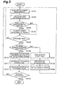
- Fig. 3 is a flow chart showing an embodiment of the thickness measuring method and wet etching method in the wet etching apparatus shown in Fig. 1.
- thickness measurement is executed at each of a plurality of measurement times t at a predetermined time interval (step S101).
- a time interval for example, a time interval of 5 Hz for the entire etching time of 1 to 2 min is set in accordance with the etching time or etching rate, and thickness measurement is automatically executed at each measurement time.
- the time interval may be constant or be changed for the entire etching time.
- the raw thickness value calculating section 16b generates a light intensity distribution (Figs. 2A and 2B).
- the calculated raw thickness value it is determined whether classification by the number of peaks of specified light intensity peaks is ON (S103). Only if YES in step S103, classification by the number of peaks is done (S104). In this classification by the number of peaks, when for each data of the calculated raw thickness value RTh(t), the number of light intensity peaks specified as peaks each having a light intensity more than the threshold value within the optical path length range set for the light intensity distribution is smaller than three, the raw thickness value is invalidated.
- Data when the number of specified peaks is smaller than three corresponds to a case wherein a measurement error has occurred because any one of the light intensity peaks P1, P2, and P3 of the liquid surface peak, wafer upper surface peak, and wafer lower surface peak is not detected.
- an erroneous raw thickness value is obtained at high probability.
- Such classification by the number of peaks is especially effective when the liquid layer E and wafer W have almost the same thickness, and it is difficult to determine whether a measurement error has occurred by applying a sorting numerical value range or allowable numerical value range (to be described later).
- step S105 it is determined whether the time that has elapsed from the initial measurement time is a specified time or more (S105). If NO in step S105, execution of thickness measurement and calculation of the raw thickness value are repeated. If YES in step S105, statistical processing of the raw thickness value is started.
- the specified time is used to determine whether the number of statistical points of raw thickness value data sufficient for thickness evaluation of the semiconductor wafer W are obtained.
- the specified time is preferably designated by the time (time width) elapsed from the initial measurement time. Alternatively, the specified time may be specified by the number of statistical points at which thickness measurement has been executed. In the following description, the specified time is designated not by the number of statistical points but by the time width.
- a time width Tc from the initial measurement time is defined as the specified time.
- step S106 it is subsequently determined whether the allowable numerical value range for the raw thickness value has already been set. If NO in step S106, it is the first measurement time after the elapse of specified time Tc from the initial measurement time, and therefore, the allowable numerical value range is set.
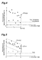
- raw thickness values RTh(t) calculated at the measurement times t shown in each graph raw thickness values that are validated at the stages of the graphs are indicated by full circles. Invalid raw thickness values are indicated by open circles or not illustrated for the illustrative convenience.
- the allowable numerical value range is set using valid data (full circles).
- Data sorting calculation of the first time is performed for a time-rate change in valid raw thickness values RTh(t) indicated by full circles in Fig. 4 (S107), as shown in Fig. 5.
- First, linear approximation (fitting calculation such as the least square method) is executed for the data of the raw thickness values RTh(t) to determine a first thickness change line FTh1(t) as an approximated line.
- the thickness change line FTh1(t) is a line for data sorting.
- a first sorting numerical value range DTh1 is set from the thickness change line FTh1(t) for sorting.
- a variation value ⁇ 1 of the raw thickness value RTh(t) is calculated for the thickness change line FTh1(t).
- the variation value ⁇ 1 of the raw thickness value for example, the value of standard deviation for the thickness change line for raw thickness value data sorting can be used.
- Data sorting of the first time for the raw thickness value is executed using the set sorting numerical value range DTh1. More specifically, raw thickness value data within the range of ⁇ DTh1 from the thickness change line FTh1(t) (indicated by two dashed lines that sandwich the thickness change line FTh1(t) for sorting from the upper and lower sides in Fig. 5) are continuously validated. In addition, raw thickness value data outside this range (five data points indicated by open circles in Fig. 5) are invalidated.
- Raw thickness value data within the range of ⁇ DTh2 from the thickness change line FTh2(t) are continuously validated.
- raw thickness value data outside this range are invalidated.
- data sorting calculation of raw thickness values of this embodiment is ended.
- An allowable numerical value range DTh is set on the basis of the time-rate change in data of raw thickness values RTh(t) that are valid after sorting by the above-described data sorting calculation, as shown in Fig. 7 (S109).
- linear approximation calculation is executed for the data of raw thickness values (eight data points indicated by full circles in Figs. 6 and 7) validated by data sorting calculation of the first and second times, thereby determining a thickness change line FTh tn (t) as an approximated line representing a time-rate change in raw thickness value.
- the subfix tn of the thickness change line indicates that the thickness change line is determined at the measurement time tn.
- the allowable numerical value range DTh from the thickness change line FTh tn (t) is set.
- the method of setting the allowable numerical value range DTh in this embodiment is almost the same as the method of setting the sorting numerical value ranges DTh1 and DTh2.
- a variation value ⁇ such as the standard deviation of the raw thickness value RTh(t) that is validated at this stage is calculated.
- the allowable numerical value range DTh set here is used to determine whether a raw thickness value at each of measurement times (second and subsequent measurement times after the elapse of the specified time Tc from the initial measurement time) is valid or invalid.
- determination of the thickness change line FTh tn (t) at the measurement time tn and setting of the allowable numerical value range DTh are ended, the processing shifts to execution of the next thickness measurement and calculation of the raw thickness value.
- the allowable numerical value range has already been set. Hence, the above-described data sorting and (re-)setting of the allowable numerical value range are not executed, and it is determined whether a raw thickness value falls within or outside the allowable range.
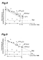
- the method of determining whether a raw thickness value falls within or outside the allowable range at second and subsequent measurement times (S110 to S112) will be described with reference to the graphs schematically shown in Figs. 8 and 9.
- the value falls within or outside the allowable range (S110), as shown in Fig. 8. More specifically, determination whether the value falls within or outside the allowable range is done by determining whether the value falls within the allowable numerical value range DTh from the thickness change line FTh tn (t) determined at the preceding measurement time (here, the measurement time tn).
- the thickness change line FTh tn (t) determined at the preceding measurement time tn is extrapolated (dotted line) to obtain an expected value FTh tn (tm) of the thickness at the current measurement time tm. If the raw thickness value RTh(tm) by thickness measurement executed at the measurement time tm falls within the range of ⁇ DTh from FTh tn (tm) (indicated by two dashed lines that sandwich the thickness change line FTh tn (t) from the upper and lower sides in Fig. 8), the data of the raw thickness value RTh(tm) is validated. Otherwise, the data of the raw thickness value is invalidated. On the basis of the determination result, the thickness change line FTh tm (t) for the current measurement time tm is determined (S111).
- the raw thickness value RTh(tm) falls within the range of the allowable numerical value range DTh from the preceding thickness change line FTh tn (t). At this time, the raw thickness value RTh(tm) is valid. As shown in Fig. 9, linear approximation calculation is executed for valid raw thickness value data (full circles) within the time range of the specified time Tc from the measurement time tm, including the raw thickness value RTh(tm), thereby determining the new thickness change line FTh tm (t).
- the raw thickness value RTh(tm) falls outside the range of the allowable numerical value range DTh from the preceding thickness change line FTh tn (t)
- the raw thickness value RTh(tm) is invalid.
- linear approximation calculation is not executed.
- the interference light between reflected light and reference light, which are generated from measurement light is detected.
- Light intensity peaks corresponding to the upper and lower surfaces of the semiconductor wafer are specified and selected in a light intensity distribution for a change in optical path length.
- Raw thickness values are calculated from the difference in optical path length between the light intensity peaks.
- data sorting calculation including preliminary linear approximation calculation for data sorting, setting of a sorting numerical value range, and data sorting is executed.
- the thickness change line is set, and the allowable numerical value range is set on the basis of valid raw thickness values after the end of data sorting calculation.
- the thickness of the semiconductor wafer W can be more accurately obtained by sufficiently and efficiently removing the influence of an error variation and the like from the thickness change line and statistical thickness value.
- determination is done for each raw thickness value on the basis of the set allowable numerical value range and the preceding thickness change line. Only when a raw thickness value is validated, new linear approximation calculation is executed, thereby realizing efficient calculation of a statistical thickness value.
- the allowable numerical value range and sorting numerical value range at the first measurement time after the elapse of the specified time are set on the basis of a variation value from the thickness change line of a raw thickness value that is valid at that time and the allowance constant and sorting constant, which are determined in advance. Since the actual state of raw thickness value data as an object is reflected in setting the allowable numerical value range and sorting numerical value range, a numerical value range appropriate for the data can be set.
- the allowable numerical value range is normally set to a numerical value range smaller than the sorting numerical value range. More specifically, in the above-described example, the first sorting numerical value range DTh1, second sorting numerical value range DTh2, and allowable numerical value range DTh normally have a relationship DTh1 > DTh2 > DTh. However, since the relationship between the numerical value ranges is mainly determined by the variation value, the allowance constant and sorting constant from which the variation value has been removed do not always have such a relationship.
- the operator or the like may directly set the numerical value ranges without designating the allowance constant and sorting constant. Even in this case, the numerical value ranges are preferably set to satisfy the above relationship. Some numerical value ranges (e.g., the second sorting numerical value range and final allowable numerical value range) may be set equal, or the allowable numerical value range may be set to be slightly wider than the sorting numerical value range, as needed.
- a raw thickness value outside the range of the specified time from that measurement time is invalidated and is not used for line determination.
- This range setting is effective in coping with a time-rate change when, e.g., the etching rate changes over time during wet etching. A more accurate thickness change line and statistical thickness value can be obtained while ensuring a sufficient number of statistical points.
- raw thickness values from the initial measurement time may always be used. In this case, the number of statistical points of raw thickness value data to be used for statistical processing increases as time elapses.
- the end of wet etching by stopping supply of the etchant from the etchant supply section 24 or the change of the etching rate can be appropriately controlled through the etching control section 25.
- the variation from the terminal thickness can be suppressed by obtaining the end time on the basis of the thickness change line and statistical thickness value, and the preset terminal thickness. Hence, the efficiency and yield in semiconductor manufacturing can be increased.
- the measurement time is set as the end time.
- an end instruction signal is output from the thickness calculating section 16 (statistical thickness value calculating section 16c) to the etching control section 25, thereby ending wet etching.
- an arrangement for predicting the end time using the thickness change line can be employed. That is, as shown in Fig. 9, the thickness change line FTh tm (t) is extrapolated (extended), and an intersection between the thickness change line and a line that indicates the terminal thickness is obtained. A time te at that intersection can be predicted as the end time. When the end time is predicted in advance, wet etching end control can be performed on the basis of the predicted end time.
- the holding substrate 21 maintains the mechanical strength of the semiconductor wafer W to be etched thin. Some semiconductor wafers W can be etched without using the holding substrate 21 depending on their thicknesses.
- the probe head 13 serving as a light output means is also used as a light input means for receiving reflected light from the semiconductor wafer W.
- a light input means may be arranged separately from the light output means.
- the reflected light is input to an optical fiber different from the optical fiber 13a to the probe head 13, the reflected light and reference light are coupled using, e.g. another optical coupler arranged in addition to the optical coupler 12.
- only one of the light input/output means or the light branching/coupling means may be formed from a single light input/output means or optical coupler, and the other means may be formed from separate means.
- the etching rate of wet etching need not always be constant.
- the thickness can more finely be controlled.
- the time range of raw thickness data in which a time-rate change in thickness is obtained may be divided, and thickness change lines may be separately obtained before and after an etching rate change time.
- the thickness measuring apparatus and thickness measuring method according to the present invention and the wet etching apparatus and wet etching method using the thickness measuring apparatus and method can be used as a thickness measuring apparatus and method and the like capable of measuring the thickness of a semiconductor wafer independently of the presence of an etchant and obtaining a statistical thickness value in which the influence of an error variation and statistical variation is sufficiently reduced by calculating the raw thickness value of the semiconductor wafer W from the optical path length difference between two light intensity peaks selected from the light intensity distribution of interference light obtained by coupling reflected light and reference light and executing statistical processing including determination about the allowable numerical value range and determination of the thickness change line and, more particularly, at the first measurement time after the elapse of the specified time, statistical processing including data sorting calculation and determination of the thickness change line.
- the actual etching rate or a time-rate change in etching rate in each wet etching process can be known by actual measurement.
- wet etching can be controlled while determining a time-rate change in thickness during etching. Hence, the efficiency and yield in semiconductor manufacturing can be increased.
Landscapes
- Physics & Mathematics (AREA)
- General Physics & Mathematics (AREA)
- Length Measuring Devices By Optical Means (AREA)
- Weting (AREA)
- Testing Or Measuring Of Semiconductors Or The Like (AREA)
- Instruments For Measurement Of Length By Optical Means (AREA)
- Length-Measuring Instruments Using Mechanical Means (AREA)
- A Measuring Device Byusing Mechanical Method (AREA)
Claims (18)
- Dispositif de mesure d'épaisseur (A) pour mesurer une épaisseur d'une plaquette en semi-conducteur (W) durant l'exécution d'une gravure humide utilisant une solution d'attaque, caractérisé en ce qu'il comprend:une source de lumière de mesure (11) pour délivrer une lumière de mesure à chacun d'une pluralité d'instants de mesure à un intervalle de temps prédéterminé ;des moyens de branchement de lumière (12) pour brancher la lumière provenant de ladite source de lumière de mesure ;des moyens de sortie de lumière (13, 13a) pour délivrer en sortie une composante de la lumière de mesure branchée par lesdits moyens de branchement de lumière à la plaquette en semi-conducteur comme un objet de mesure de manière à irradier la plaquette en semi-conducteur à partir d'un côté d'une surface de gravure sur laquelle la solution d'attaque est délivrée ;des moyens d'entrée de lumière (13, 13a) pour entrer une lumière réfléchie obtenue quand la lumière de mesure irradiée à partir desdits moyens de sortie de lumière est réfléchie par la solution d'attaque ou la plaquette en semi-conducteur ;des moyens de génération de lumière de référence (14, 17) pour faire passer l'autre composante de la lumière de mesure branchée par lesdits moyens de branchement de lumière à travers un parcours optique de référence conçu pour être capable de changer une longueur de parcours optique de manière à générer une lumière de référence pour laquelle une longueur de parcours optique de référence est fixée ;des moyens de couplage de lumière (12) pour obtenir une lumière d'interférence en couplant la lumière réfléchie provenant desdits moyens d'entrée de lumière à la lumière de référence provenant desdits moyens de génération de lumière de référence ;des moyens de photodétection (15) pour détecter la lumière d'interférence provenant desdits moyens de couplage de lumière ;des moyens de calcul de valeur d'épaisseur brute (16b) pour calculer une valeur d'épaisseur brute de la plaquette en semi-conducteur sur la base d'une différence de longueur de parcours optique dans une longueur de parcours optique de référence entre deux pics d'intensité lumineuse sélectionnés à partir d'une pluralité de pics d'intensité lumineuse ayant chacun une intensité lumineuse supérieure à une valeur de seuil fixée, en utilisant une distribution d'intensité lumineuse représentant une corrélation entre la longueur de parcours optique de référence fixée par lesdits moyens de génération de lumière de référence et une intensité lumineuse de la lumière d'interférence détectée par lesdits moyens de photodétection à chacun des instants de mesure ; etdes moyens de calcul de valeur d'épaisseur statistique (16c) pour, à chacun des instants de mesure après un écoulement d'un temps spécifié à partir d'un instant de mesure initial, déterminer une ligne de changement d'épaisseur par approximation linéaire pour un changement taux-temps d'une pluralité de valeurs d'épaisseur brutes valides dans une plage de valeurs numériques admissibles fixée de manière à calculer une valeur d'épaisseur statistique à partir de la ligne de changement d'épaisseur,dans lequel au premier instant de mesure après l'écoulement du temps spécifié à partir d'un instant de mesure initial, lesdits moyens de calcul de valeur d'épaisseur statistique sont agencés pour exécuter, pour le changement taux-temps de valeur d'épaisseur brute valide avant ledit premier instant de mesure après ledit écoulement, un calcul de tri de données comprenant la détermination d'une ligne de changement d'épaisseur pour le tri par approximation linéaire, une détermination d'une plage de valeurs numériques de tri pour la ligne de changement d'épaisseur pour le tri et un tri de données pour lesquelles la valeur d'épaisseur brute à l'extérieur de la plage de valeurs numériques de tri est destinée à être invalidée, pour déterminer ensuite la ligne de changement d'épaisseur par approximation linéaire pour le changement taux-temps de valeur d'épaisseur brute valide après tri et pour déterminer la plage de valeurs numériques admissibles à partir de la ligne de changement d'épaisseur.
- Dispositif de mesure d'épaisseur selon la revendication 1, caractérisé en ce que
à chacun du deuxième instant de mesure et suivants après l'écoulement du temps spécifié à partir de l'instant de mesure initial, lesdits moyens de calcul de valeur d'épaisseur statistique déterminent, sur la base du fait que la valeur d'épaisseur brute calculée à l'instant de mesure se trouve à l'intérieur ou à l'extérieur d'une plage de la plage de valeurs numériques admissibles à partir de la ligne de changement d'épaisseur déterminée à l'instant de mesure précédent, que la valeur d'épaisseur brute est valide ou non valide,
quand la valeur d'épaisseur brute calculée se trouve à l'intérieur de la plage de valeurs numériques admissibles et est considérée comme valide, déterminent la ligne de changement d'épaisseur par approximation linéaire pour le changement taux-temps de la pluralité de valeurs d'épaisseur brutes valides incluant la valeur d'épaisseur brute et calcule la valeur d'épaisseur statistique à partir de la ligne de changement d'épaisseur, et
quand la valeur d'épaisseur brute calculée se trouve à l'extérieur de la plage de valeurs numériques admissibles et est considérée comme non valide, déterminent la ligne de changement d'épaisseur déterminée à l'instant de mesure précédent comme la ligne de changement d'épaisseur à l'instant actuel et calcule la valeur d'épaisseur statistique à partir de la ligne de changement d'épaisseur. - Dispositif de mesure d'épaisseur selon la revendication 1 ou 2, caractérisé en ce que
au premier instant de mesure après l'écoulement du temps spécifié à partir de l'instant de mesure initial, lesdits moyens de calcul de valeur d'épaisseur statistique fixent la plage de valeurs numériques admissibles à une plage de valeurs numériques plus étroites que la plage de valeurs numériques de tri. - Dispositif de mesure d'épaisseur selon l'une quelconque des revendications 1 à 3, caractérisé en ce que
au premier instant de mesure après l'écoulement du temps spécifié à partir de l'instant de mesure initial, lesdits moyens de calcul de valeur d'épaisseur statistique fixent la plage de valeurs numériques de tri sur la base d'une valeur de variation de la valeur d'épaisseur brute à trier à partir de la ligne de changement d'épaisseur pour le tri et d'une constante de tri prédéterminée, et
fixent la plage de valeurs numériques admissibles sur la base d'une valeur de variation de la valeur d'épaisseur brute valide après tri à partir de la ligne de changement d'épaisseur pour le tri et d'une constante de tri prédéterminée. - Dispositif de mesure d'épaisseur selon l'une quelconque des revendications 1 à 4, caractérisé en ce que lesdits moyens de calcul de valeur d'épaisseur statistique invalident la valeur d'épaisseur brute quand le nombre de pics d'intensité lumineuse est inférieur à trois à chacun des instants de mesure.
- Dispositif de mesure d'épaisseur selon l'une quelconque des revendications 1 à 5, caractérisé en ce que
à chacun du deuxième instant de mesure et suivants après l'écoulement du temps spécifié à partir de l'instant de mesure initial, lesdits moyens de calcul de valeur d'épaisseur statistique invalident la valeur d'épaisseur brute à l'extérieur de la plage du temps spécifié à partir de l'instant de mesure. - Dispositif de gravure humide ayant ledit dispositif de mesure d'épaisseur selon l'une quelconque des revendications 1 à 6, caractérisé en ce qu'il comprend:des moyens d'alimentation de solution d'attaque pour délivrer la solution d'attaque sur la surface de gravure de la plaquette en semi-conducteur comme un objet de la gravure humide ; etdes moyens de commande de gravure pour commander l'alimentation de solution d'attaque par lesdits moyens d'alimentation de solution d'attaque.
- Dispositif de gravure humide selon la revendication 7, caractérisé en ce que
lesdits moyens de calcul de valeur d'épaisseur statistique dudit dispositif de mesure d'épaisseur obtiennent un instant de fin de gravure humide sur la base d'une épaisseur finale prédéterminée à partir de la ligne de changement d'épaisseur déterminée et délivre en sortie un signal d'instruction de fin pour donner instruction de l'instant de fin, et
lesdits moyens de commande de gravure forcent lesdits moyens d'alimentation de solution d'attaque à arrêter l'alimentation de la solution d'attaque sur la base du signal d'instruction de fin. - Procédé de mesure d'épaisseur pour mesurer une épaisseur d'une plaquette en semi-conducteur durant l'exécution d'une gravure humide utilisant une solution d'attaque, caractérisé en ce qu'il comprend :une étape d'alimentation de lumière de mesure pour délivrer une lumière de mesure provenant d'une source de lumière de mesure à chacun d'une pluralité d'instants de mesure à un intervalle de temps prédéterminé ;une étape de branchement de lumière pour brancher la lumière provenant de la source de lumière de mesure ;une étape de sortie de lumière pour délivrer en sortie une composante de la lumière de mesure branchée dans l'étape de branchement de lumière à la plaquette en semi-conducteur comme un objet de mesure de manière à irradier la plaquette en semi-conducteur à partir d'un côté d'une surface de gravure sur laquelle la solution d'attaque est délivrée ;une étape d'entrée de lumière pour entrer une lumière réfléchie obtenue quand la lumière de mesure irradiée à partir desdits moyens de sortie de lumière est réfléchie par la solution d'attaque ou la plaquette en semi-conducteur ;une étape de génération de lumière de référence pour faire passer l'autre composante de la lumière de mesure branchée dans l'étape de branchement de lumière à travers un parcours optique de référence conçu pour être capable de changer une longueur de parcours optique de manière à générer une lumière de référence pour laquelle une longueur de parcours optique de référence est fixée ;une étape de couplage de lumière pour obtenir une lumière d'interférence en couplant la lumière réfléchie entrée dans l'étape d'entrée de lumière à la lumière de référence générée dans l'étape de génération de lumière de référence ;une étape de photodétection pour détecter la lumière d'interférence couplée dans l'étape de couplage de lumière ;une étape de calcul de valeur d'épaisseur brute pour calculer une valeur d'épaisseur brute de la plaquette en semi-conducteur sur la base d'une différence longueur de parcours optique dans une longueur de parcours optique de référence entre deux pics d'intensité lumineuse sélectionnés à partir d'une pluralité de pics d'intensité lumineuse ayant chacun une intensité lumineuse supérieure à une valeur de seuil fixée, en utilisant une distribution d'intensité lumineuse représentant une corrélation entre la longueur de parcours optique de référence fixée dans l'étape de génération de lumière de référence et une intensité lumineuse de la lumière d'interférence détectée dans l'étape de photodétection à chacun des instants de mesure ; etune étape de calcul de valeur d'épaisseur statistique consistant, à chacun des instants de mesure après un écoulement d'un temps spécifié à partir d'un instant de mesure initial, à déterminer une ligne de changement d'épaisseur par approximation linéaire pour un changement taux-temps d'une pluralité de valeurs d'épaisseur brutes valides dans une plage de valeurs numériques admissibles fixée de manière à calculer une valeur d'épaisseur statistique à partir de la ligne de changement d'épaisseur,dans lequel dans l'étape de calcul de valeur d'épaisseur statistique, au premier instant de mesure après l'écoulement du temps spécifié à partir d'un instant de mesure initial, pour le changement taux-temps de valeur d'épaisseur brute valide avant ledit premier instant de mesure après ledit écoulement, un calcul de tri de données comprenant la détermination d'une ligne de changement d'épaisseur pour le tri par approximation linéaire, une détermination d'une plage de valeurs numériques de tri pour la ligne de changement d'épaisseur pour le tri et un tri de données pour lesquelles la valeur d'épaisseur brute à l'extérieur de la plage de valeurs numériques de tri est destinée à être invalidée sont exécutés, et dans lequel ensuite la ligne de changement d'épaisseur par approximation linéaire pour le changement taux-temps de valeur d'épaisseur brute valide après tri et pour déterminer la plage de valeurs numériques admissibles à partir de la ligne de changement d'épaisseur est fixée.
- Procédé de mesure d'épaisseur selon la revendication 9, caractérisé en ce que
dans l'étape de calcul de valeur d'épaisseur statistique, à chacun du deuxième instant de mesure et suivants après l'écoulement du temps spécifié à partir de l'instant de mesure initial, il est déterminé, sur la base du fait que la valeur d'épaisseur brute calculée à l'instant de mesure se trouve à l'intérieur ou à l'extérieur d'une plage de la plage de valeurs numériques admissibles à partir de la ligne de changement d'épaisseur déterminée à l'instant de mesure précédent, que la valeur d'épaisseur brute est valide ou non valide,
quand la valeur d'épaisseur brute calculée se trouve à l'intérieur de la plage de valeurs numériques admissibles et est considérée comme valide, la ligne de changement d'épaisseur par approximation linéaire est déterminée pour le changement taux-temps de la pluralité de valeurs d'épaisseur brutes valides incluant la valeur d'épaisseur brute et la valeur d'épaisseur statistique est calculée à partir de la ligne de changement d'épaisseur, et
quand la valeur d'épaisseur brute calculée se trouve à l'extérieur de la plage de valeurs numériques admissibles et est considérée comme non valide, la ligne de changement d'épaisseur déterminée à l'instant de mesure précédent est déterminée comme la ligne de changement d'épaisseur à l'instant actuel et la valeur d'épaisseur statistique est calculée à partir de la ligne de changement d'épaisseur. - Procédé de mesure d'épaisseur selon la revendication 9 ou 10, caractérisé en ce que
dans l'étape de calcul de valeur d'épaisseur statistique, au premier instant de mesure après l'écoulement du temps spécifié à partir de l'instant de mesure initial, la plage de valeurs numériques admissibles est fixée à une plage de valeurs numériques plus étroites que la plage de valeurs numériques de tri. - Procédé de mesure d'épaisseur selon l'une quelconque des revendications 9 à 11, caractérisé en ce que
dans l'étape de calcul de valeur d'épaisseur statistique, au premier instant de mesure après l'écoulement du temps spécifié à partir de l'instant de mesure initial, la plage de valeurs numériques de tri est fixée sur la base d'une valeur de variation de la valeur d'épaisseur brute à trier à partir de la ligne de changement d'épaisseur pour le tri et d'une constante de tri prédéterminée, et
la plage de valeurs numériques admissibles est fixée sur la base d'une valeur de variation de la valeur d'épaisseur brute valide après tri à partir de la ligne de changement d'épaisseur pour le tri et d'une constante de tri prédéterminée. - Dispositif de mesure d'épaisseur selon l'une quelconque des revendications 9 à 12, caractérisé en ce que lesdits moyens de calcul de valeur d'épaisseur statistique invalident la valeur d'épaisseur brute quand le nombre de pics d'intensité lumineuse est inférieur à trois à chacun des instants de mesure.
- Dispositif de mesure d'épaisseur selon l'une quelconque des revendications 9 à 13, caractérisé en ce que
dans l'étape de calcul de valeur d'épaisseur statistique, à chacun du deuxième instant de mesure et suivants après l'écoulement du temps spécifié à partir de l'instant de mesure initial, la valeur d'épaisseur brute à l'extérieur de la plage du temps spécifié à partir de l'instant de mesure est invalidée. - Procédé de gravure humide comprenant le procédé de mesure d'épaisseur selon l'une quelconque des revendications 9 à 14, caractérisé en ce qu'il comprend :l'étape de début de gravure consistant à délivrer la solution d'attaque sur la surface de gravure de la plaquette en semi-conducteur comme un objet de gravure humide de manière à démarrer la gravure humide ; etl'étape de mesure d'épaisseur consistant à mesurer une épaisseur de la plaquette en semi-conducteur par le procédé de mesure d'épaisseur durant l'exécution d'une gravure humide démarrée dans l'étape de début de gravure à chacun des instants de mesure à l'intervalle de temps ; etl'étape de fin de gravure consistant à arrêter l'alimentation de la solution d'attaque pour terminer la gravure humide.
- Procédé de gravure humide selon la revendication 15, caractérisé en ce qu'il comprend en outre l'étape de calcul de l'instant de fin consistant à obtenir un temps de fin de gravure humide sur la base d'une épaisseur finale prédéterminée à partir de la ligne de changement d'épaisseur déterminée dans l'étape de mesure d'épaisseur, et dans lequel
dans l'étape de fin de gravure, l'alimentation de la solution d'attaque est arrêtée sur la base de l'instant de fin obtenu dans l'étape de calcul de l'instant de fin. - Procédé de gravure humide selon la revendication 16, caractérisé en ce que, dans l'étape de calcul de l'instant de fin, l'instant de mesure quand la valeur d'épaisseur statistique calculée à partir de la ligne de changement d'épaisseur n'est pas supérieure à l'épaisseur terminale est obtenu comme le temps de fin.
- Procédé de gravure humide selon la revendication 16, caractérisé en ce que, dans l'étape de calcul de l'instant de fin, le temps de fin est prédit en utilisant la ligne de changement d'épaisseur.
Applications Claiming Priority (3)
| Application Number | Priority Date | Filing Date | Title |
|---|---|---|---|
| JP2000132607A JP4486217B2 (ja) | 2000-05-01 | 2000-05-01 | 厚み計測装置、及びそれを用いたウエットエッチング装置、ウエットエッチング方法 |
| JP2000132607 | 2000-05-01 | ||
| PCT/JP2001/000351 WO2001084620A1 (fr) | 2000-05-01 | 2001-01-19 | Dispositif et procede de mesure d'epaisseur, dispositif et procede de gravure humide utilisant les precedents |
Publications (3)
| Publication Number | Publication Date |
|---|---|
| EP1296367A1 EP1296367A1 (fr) | 2003-03-26 |
| EP1296367A4 EP1296367A4 (fr) | 2005-06-15 |
| EP1296367B1 true EP1296367B1 (fr) | 2007-04-04 |
Family
ID=18641274
Family Applications (1)
| Application Number | Title | Priority Date | Filing Date |
|---|---|---|---|
| EP01901468A Expired - Lifetime EP1296367B1 (fr) | 2000-05-01 | 2001-01-19 | Dispositif et procede de mesure d'epaisseur, dispositif et procede de gravure humide utilisant les precedents |
Country Status (7)
| Country | Link |
|---|---|
| US (1) | US6768552B2 (fr) |
| EP (1) | EP1296367B1 (fr) |
| JP (1) | JP4486217B2 (fr) |
| AT (1) | ATE358892T1 (fr) |
| AU (1) | AU2001227075A1 (fr) |
| DE (1) | DE60127673T2 (fr) |
| WO (1) | WO2001084620A1 (fr) |
Families Citing this family (47)
| Publication number | Priority date | Publication date | Assignee | Title |
|---|---|---|---|---|
| ATE396497T1 (de) * | 2000-01-21 | 2008-06-15 | Hamamatsu Photonics Kk | Dickenmessvorrichtung, dickenmessverfahren und nassätzvorrichtung und nassätzverfahren, die diese verwenden |
| GB2404787B (en) * | 2000-07-05 | 2005-04-13 | Metryx Ltd | Apparatus and method for investigating semiconductor wafers |
| GB0016562D0 (en) | 2000-07-05 | 2000-08-23 | Metryx Limited | Apparatus and method for investigating semiconductor wafers |
| JP2003307458A (ja) * | 2002-04-15 | 2003-10-31 | Akifumi Ito | 基材の温度測定方法および温度測定装置 |
| JP2003315017A (ja) * | 2002-04-25 | 2003-11-06 | Hamamatsu Photonics Kk | 厚み計測装置 |
| US7116429B1 (en) * | 2003-01-18 | 2006-10-03 | Walecki Wojciech J | Determining thickness of slabs of materials by inventors |
| US7256104B2 (en) * | 2003-05-21 | 2007-08-14 | Canon Kabushiki Kaisha | Substrate manufacturing method and substrate processing apparatus |
| JP4364242B2 (ja) * | 2004-03-22 | 2009-11-11 | 三益半導体工業株式会社 | スピンエッチングにおける工程管理方法及びスピンエッチング装置 |
| DE102004045956B4 (de) * | 2004-09-22 | 2008-12-11 | Universität des Saarlandes | Ätzhalterung für ein Substrat und Ätzsystem mit einer Ätzhalterung |
| US7502121B1 (en) * | 2004-11-24 | 2009-03-10 | Ahbee 1, L.P. | Temperature insensitive low coherence based optical metrology for nondestructive characterization of physical characteristics of materials |
| FR2892188B1 (fr) | 2005-10-14 | 2007-12-28 | Nanotec Solution Soc Civ Ile | Procede et dispositif de mesure de hauteurs de motifs |
| JP2008012542A (ja) * | 2006-07-03 | 2008-01-24 | Hamamatsu Photonics Kk | レーザ加工方法 |
| JP4939304B2 (ja) * | 2007-05-24 | 2012-05-23 | 東レエンジニアリング株式会社 | 透明膜の膜厚測定方法およびその装置 |
| GB0719469D0 (en) | 2007-10-04 | 2007-11-14 | Metryx Ltd | Measurement apparatus and method |
| GB0719460D0 (en) | 2007-10-04 | 2007-11-14 | Metryx Ltd | Measurement apparatus and method |
| DE102007048295A1 (de) | 2007-10-08 | 2009-04-16 | Precitec Optronik Gmbh | Vorrichtung und Verfahren zur Dickenmessung |
| JP5112930B2 (ja) * | 2008-03-28 | 2013-01-09 | 浜松ホトニクス株式会社 | 厚み計測装置 |
| IT1391719B1 (it) * | 2008-11-17 | 2012-01-27 | Marposs Spa | Metodo, stazione ed apparecchiatura per la misura ottica mediante interferometria dello spessore di un oggetto |
| GB2478590A (en) | 2010-03-12 | 2011-09-14 | Precitec Optronik Gmbh | Apparatus and method for monitoring a thickness of a silicon wafer |
| IT1399876B1 (it) * | 2010-05-18 | 2013-05-09 | Marposs Spa | Metodo e apparecchiatura per la misura ottica mediante interferometria dello spessore di un oggetto |
| IT1399875B1 (it) * | 2010-05-18 | 2013-05-09 | Marposs Spa | Metodo e apparecchiatura per la misura ottica mediante interferometria dello spessore di un oggetto |
| SG185368A1 (en) * | 2010-05-18 | 2012-12-28 | Marposs Spa | Method and apparatus for optically measuring by interferometry the thickness of an object |
| EP3793175A1 (fr) | 2010-11-19 | 2021-03-17 | IOT Holdings, Inc. | Procédures d'interface de communication entre machines (m2m) servant à annoncer et désannoncer des ressources |
| JP5853382B2 (ja) * | 2011-03-11 | 2016-02-09 | ソニー株式会社 | 半導体装置の製造方法、及び電子機器の製造方法 |
| GB2489722B (en) * | 2011-04-06 | 2017-01-18 | Precitec Optronik Gmbh | Apparatus and method for determining a depth of a region having a high aspect ratio that protrudes into a surface of a semiconductor wafer |
| DE102011051146B3 (de) | 2011-06-17 | 2012-10-04 | Precitec Optronik Gmbh | Prüfverfahren zum Prüfen einer Verbindungsschicht zwischen waferförmigen Proben |
| JP2013130417A (ja) * | 2011-12-20 | 2013-07-04 | Nippon Electric Glass Co Ltd | ガラス板の反り測定方法およびガラス板の製造方法 |
| CN202601580U (zh) * | 2012-03-31 | 2012-12-12 | 北京京东方光电科技有限公司 | 一种刻蚀时间检测装置及刻蚀设备 |
| DE102012111008B4 (de) | 2012-11-15 | 2014-05-22 | Precitec Optronik Gmbh | Optisches Messverfahren und optische Messvorrichtung zum Erfassen einer Oberflächentopographie |
| TWI638131B (zh) | 2013-06-17 | 2018-10-11 | 普雷茨特光電有限公司 | 用於獲取距離差之光學量測裝置及光學量測方法 |
| JP6289930B2 (ja) * | 2014-02-18 | 2018-03-07 | 株式会社ディスコ | ウェットエッチング装置 |
| US10551165B2 (en) | 2015-05-01 | 2020-02-04 | Adarza Biosystems, Inc. | Methods and devices for the high-volume production of silicon chips with uniform anti-reflective coatings |
| US10207489B2 (en) * | 2015-09-30 | 2019-02-19 | Sigma Labs, Inc. | Systems and methods for additive manufacturing operations |
| TWI629720B (zh) * | 2015-09-30 | 2018-07-11 | Tokyo Electron Limited | 用於濕蝕刻製程之溫度的動態控制之方法及設備 |
| JP2018024571A (ja) * | 2016-08-05 | 2018-02-15 | 旭硝子株式会社 | 孔を有するガラス基板の製造方法 |
| US10234265B2 (en) | 2016-12-12 | 2019-03-19 | Precitec Optronik Gmbh | Distance measuring device and method for measuring distances |
| CN110383428B (zh) * | 2017-03-10 | 2023-04-04 | 三菱电机株式会社 | 半导体制造装置以及半导体制造方法 |
| DE102017126310A1 (de) | 2017-11-09 | 2019-05-09 | Precitec Optronik Gmbh | Abstandsmessvorrichtung |
| WO2020070884A1 (fr) * | 2018-10-05 | 2020-04-09 | 三菱電機株式会社 | Dispositif d'usinage |
| DE102018130901A1 (de) | 2018-12-04 | 2020-06-04 | Precitec Optronik Gmbh | Optische Messeinrichtung |
| JP7166966B2 (ja) | 2019-03-15 | 2022-11-08 | 株式会社Screenホールディングス | 処理条件選択方法、基板処理方法、基板製品製造方法、処理条件選択装置、コンピュータープログラム、および、記憶媒体 |
| PL3786574T3 (pl) * | 2019-08-26 | 2025-03-31 | Sturm Maschinen- & Anlagenbau Gmbh | Urządzenie czujnikowe |
| CN110690134B (zh) * | 2019-09-12 | 2022-07-01 | 长江存储科技有限责任公司 | 多站式沉积工艺的串气检测方法、设备及可读存储介质 |
| EP4168734B1 (fr) | 2020-06-19 | 2025-09-24 | Precitec Optronik GmbH | Appareil de mesure confocal chromatique |
| CN114038777B (zh) * | 2022-01-11 | 2022-04-08 | 江苏卓远半导体有限公司 | 一种半导体晶片测厚设备 |
| DE102024202639A1 (de) * | 2024-03-20 | 2025-09-25 | Semsysco Gmbh | System und Verfahren zur nasschemischen Behandlung einer Substratoberfläche |
| CN117968545B (zh) * | 2024-03-28 | 2024-09-24 | 钛玛科(北京)工业科技有限公司 | 带花纹发泡棉的厚度测量方法及系统 |
Family Cites Families (10)
| Publication number | Priority date | Publication date | Assignee | Title |
|---|---|---|---|---|
| US5490849A (en) * | 1990-07-13 | 1996-02-13 | Smith; Robert F. | Uniform-radiation caustic surface for photoablation |
| DE69208413T2 (de) * | 1991-08-22 | 1996-11-14 | Kla Instr Corp | Gerät zur automatischen Prüfung von Photomaske |
| US5220405A (en) * | 1991-12-20 | 1993-06-15 | International Business Machines Corporation | Interferometer for in situ measurement of thin film thickness changes |
| JP2831882B2 (ja) * | 1992-09-11 | 1998-12-02 | リソテック ジャパン 株式会社 | エッチングパターンの作成方法 |
| US5392124A (en) * | 1993-12-17 | 1995-02-21 | International Business Machines Corporation | Method and apparatus for real-time, in-situ endpoint detection and closed loop etch process control |
| US5956142A (en) * | 1997-09-25 | 1999-09-21 | Siemens Aktiengesellschaft | Method of end point detection using a sinusoidal interference signal for a wet etch process |
| US6282309B1 (en) * | 1998-05-29 | 2001-08-28 | Kla-Tencor Corporation | Enhanced sensitivity automated photomask inspection system |
| JPH11354489A (ja) * | 1998-06-05 | 1999-12-24 | Toshiba Corp | 半導体製造装置及び半導体装置のエッチング方法 |
| US6283829B1 (en) * | 1998-11-06 | 2001-09-04 | Beaver Creek Concepts, Inc | In situ friction detector method for finishing semiconductor wafers |
| US6160336A (en) * | 1999-11-19 | 2000-12-12 | Baker, Jr.; Robert M. L. | Peak power energy storage device and gravitational wave generator |
-
2000
- 2000-05-01 JP JP2000132607A patent/JP4486217B2/ja not_active Expired - Lifetime
-
2001
- 2001-01-19 EP EP01901468A patent/EP1296367B1/fr not_active Expired - Lifetime
- 2001-01-19 AU AU2001227075A patent/AU2001227075A1/en not_active Abandoned
- 2001-01-19 DE DE60127673T patent/DE60127673T2/de not_active Expired - Lifetime
- 2001-01-19 AT AT01901468T patent/ATE358892T1/de active
- 2001-01-19 WO PCT/JP2001/000351 patent/WO2001084620A1/fr not_active Ceased
- 2001-01-19 US US10/275,136 patent/US6768552B2/en not_active Expired - Lifetime
Also Published As
| Publication number | Publication date |
|---|---|
| AU2001227075A1 (en) | 2001-11-12 |
| DE60127673T2 (de) | 2007-12-27 |
| WO2001084620A1 (fr) | 2001-11-08 |
| ATE358892T1 (de) | 2007-04-15 |
| JP2001313279A (ja) | 2001-11-09 |
| EP1296367A4 (fr) | 2005-06-15 |
| EP1296367A1 (fr) | 2003-03-26 |
| JP4486217B2 (ja) | 2010-06-23 |
| US20030121889A1 (en) | 2003-07-03 |
| DE60127673D1 (de) | 2007-05-16 |
| US6768552B2 (en) | 2004-07-27 |
Similar Documents
| Publication | Publication Date | Title |
|---|---|---|
| EP1296367B1 (fr) | Dispositif et procede de mesure d'epaisseur, dispositif et procede de gravure humide utilisant les precedents | |
| US6897964B2 (en) | Thickness measuring apparatus, thickness measuring method, and wet etching apparatus and wet etching method utilizing them | |
| US6110752A (en) | Optical techniques of measuring endpoint during the processing of material layers in an optically hostile environment | |
| US6413147B1 (en) | Optical techniques of measuring endpoint during the processing of material layers in an optically hostile environment | |
| KR100329891B1 (ko) | 폴리싱 방법 및 장치와 이를 모니터링하는 방법 | |
| US5465154A (en) | Optical monitoring of growth and etch rate of materials | |
| KR100795616B1 (ko) | 상이한 파장을 갖는 광선으로 종료점을 검출하는 방법 및장치 | |
| KR101504508B1 (ko) | 연마 엔드포인트들을 결정하기 위한 스펙트럼 사용 | |
| KR102758311B1 (ko) | 연마 방법 및 연마 장치 | |
| US10256104B2 (en) | Film thickness measuring method, film thickness measuring apparatus, polishing method, and polishing apparatus | |
| JP4347517B2 (ja) | 厚み計測装置、及びそれを用いたウエットエッチング装置、ウエットエッチング方法 | |
| TWI412894B (zh) | 光學式異物檢測裝置及搭載該檢測裝置之處理液塗佈裝置 | |
| JP2002011655A (ja) | 半導体ウェハの研磨終了点検出装置及びその方法 | |
| JP4347484B2 (ja) | 厚み計測装置、及びそれを用いたウエットエッチング装置、ウエットエッチング方法 | |
| KR101379915B1 (ko) | 종말점 검출 장치 및 이를 구비한 식각 장치 그리고 종말점검출방법 | |
| JPH0691045B2 (ja) | エツチングモニタ−装置 | |
| JP2024093432A (ja) | 基板研磨装置 | |
| JPH09298174A (ja) | 研磨方法及びそれを用いた研磨装置 | |
| JP2002246352A (ja) | Cmp終点検出装置、cmp終点検出方法、及びcmp研磨面モニタ方法 | |
| JPH09298175A (ja) | 研磨方法及びそれを用いた研磨装置 | |
| JP2004134540A (ja) | ドライエッチング装置および終点検出方法 | |
| KR20040002052A (ko) | 포토레지스트막 두께 결정 시스템 및 방법 |
Legal Events
| Date | Code | Title | Description |
|---|---|---|---|
| PUAI | Public reference made under article 153(3) epc to a published international application that has entered the european phase |
Free format text: ORIGINAL CODE: 0009012 |
|
| 17P | Request for examination filed |
Effective date: 20021125 |
|
| AK | Designated contracting states |
Kind code of ref document: A1 Designated state(s): AT BE CH CY DE DK ES FI FR GB GR IE IT LI LU MC NL PT SE TR |
|
| RBV | Designated contracting states (corrected) |
Designated state(s): AT DE FR GB IT SE |
|
| A4 | Supplementary search report drawn up and despatched |
Effective date: 20050504 |
|
| RIC1 | Information provided on ipc code assigned before grant |
Ipc: 7H 01L 21/306 B Ipc: 7H 01L 21/66 A Ipc: 7G 01B 11/02 B Ipc: 7G 01B 11/06 B |
|
| GRAP | Despatch of communication of intention to grant a patent |
Free format text: ORIGINAL CODE: EPIDOSNIGR1 |
|
| GRAS | Grant fee paid |
Free format text: ORIGINAL CODE: EPIDOSNIGR3 |
|
| GRAA | (expected) grant |
Free format text: ORIGINAL CODE: 0009210 |
|
| AK | Designated contracting states |
Kind code of ref document: B1 Designated state(s): AT DE FR GB IT SE |
|
| REG | Reference to a national code |
Ref country code: GB Ref legal event code: FG4D |
|
| REF | Corresponds to: |
Ref document number: 60127673 Country of ref document: DE Date of ref document: 20070516 Kind code of ref document: P |
|
| REG | Reference to a national code |
Ref country code: SE Ref legal event code: TRGR |
|
| PLBE | No opposition filed within time limit |
Free format text: ORIGINAL CODE: 0009261 |
|
| STAA | Information on the status of an ep patent application or granted ep patent |
Free format text: STATUS: NO OPPOSITION FILED WITHIN TIME LIMIT |
|
| 26N | No opposition filed |
Effective date: 20080107 |
|
| PGFP | Annual fee paid to national office [announced via postgrant information from national office to epo] |
Ref country code: SE Payment date: 20140113 Year of fee payment: 14 |
|
| PGFP | Annual fee paid to national office [announced via postgrant information from national office to epo] |
Ref country code: FR Payment date: 20140108 Year of fee payment: 14 Ref country code: IT Payment date: 20140120 Year of fee payment: 14 |
|
| PGFP | Annual fee paid to national office [announced via postgrant information from national office to epo] |
Ref country code: GB Payment date: 20140115 Year of fee payment: 14 |
|
| REG | Reference to a national code |
Ref country code: SE Ref legal event code: EUG |
|
| GBPC | Gb: european patent ceased through non-payment of renewal fee |
Effective date: 20150119 |
|
| PG25 | Lapsed in a contracting state [announced via postgrant information from national office to epo] |
Ref country code: GB Free format text: LAPSE BECAUSE OF NON-PAYMENT OF DUE FEES Effective date: 20150119 |
|
| REG | Reference to a national code |
Ref country code: FR Ref legal event code: ST Effective date: 20150930 |
|
| PG25 | Lapsed in a contracting state [announced via postgrant information from national office to epo] |
Ref country code: SE Free format text: LAPSE BECAUSE OF NON-PAYMENT OF DUE FEES Effective date: 20150120 Ref country code: FR Free format text: LAPSE BECAUSE OF NON-PAYMENT OF DUE FEES Effective date: 20150202 |
|
| PG25 | Lapsed in a contracting state [announced via postgrant information from national office to epo] |
Ref country code: IT Free format text: LAPSE BECAUSE OF NON-PAYMENT OF DUE FEES Effective date: 20150119 |
|
| PGFP | Annual fee paid to national office [announced via postgrant information from national office to epo] |
Ref country code: DE Payment date: 20200107 Year of fee payment: 20 Ref country code: AT Payment date: 20191227 Year of fee payment: 20 |
|
| REG | Reference to a national code |
Ref country code: DE Ref legal event code: R071 Ref document number: 60127673 Country of ref document: DE |
|
| REG | Reference to a national code |
Ref country code: AT Ref legal event code: MK07 Ref document number: 358892 Country of ref document: AT Kind code of ref document: T Effective date: 20210119 |