EP0396099B1 - Anordnung zum Abtragen von Material eines Targets - Google Patents
Anordnung zum Abtragen von Material eines Targets Download PDFInfo
- Publication number
- EP0396099B1 EP0396099B1 EP90108262A EP90108262A EP0396099B1 EP 0396099 B1 EP0396099 B1 EP 0396099B1 EP 90108262 A EP90108262 A EP 90108262A EP 90108262 A EP90108262 A EP 90108262A EP 0396099 B1 EP0396099 B1 EP 0396099B1
- Authority
- EP
- European Patent Office
- Prior art keywords
- target
- arrangement
- cylinder
- axis
- laser
- Prior art date
- Legal status (The legal status is an assumption and is not a legal conclusion. Google has not performed a legal analysis and makes no representation as to the accuracy of the status listed.)
- Expired - Lifetime
Links
Images
Classifications
-
- H—ELECTRICITY
- H10—SEMICONDUCTOR DEVICES; ELECTRIC SOLID-STATE DEVICES NOT OTHERWISE PROVIDED FOR
- H10N—ELECTRIC SOLID-STATE DEVICES NOT OTHERWISE PROVIDED FOR
- H10N60/00—Superconducting devices
- H10N60/01—Manufacture or treatment
- H10N60/0268—Manufacture or treatment of devices comprising copper oxide
- H10N60/0296—Processes for depositing or forming copper oxide superconductor layers
- H10N60/0521—Processes for depositing or forming copper oxide superconductor layers by pulsed laser deposition, e.g. laser sputtering
-
- C—CHEMISTRY; METALLURGY
- C23—COATING METALLIC MATERIAL; COATING MATERIAL WITH METALLIC MATERIAL; CHEMICAL SURFACE TREATMENT; DIFFUSION TREATMENT OF METALLIC MATERIAL; COATING BY VACUUM EVAPORATION, BY SPUTTERING, BY ION IMPLANTATION OR BY CHEMICAL VAPOUR DEPOSITION, IN GENERAL; INHIBITING CORROSION OF METALLIC MATERIAL OR INCRUSTATION IN GENERAL
- C23C—COATING METALLIC MATERIAL; COATING MATERIAL WITH METALLIC MATERIAL; SURFACE TREATMENT OF METALLIC MATERIAL BY DIFFUSION INTO THE SURFACE, BY CHEMICAL CONVERSION OR SUBSTITUTION; COATING BY VACUUM EVAPORATION, BY SPUTTERING, BY ION IMPLANTATION OR BY CHEMICAL VAPOUR DEPOSITION, IN GENERAL
- C23C14/00—Coating by vacuum evaporation, by sputtering or by ion implantation of the coating forming material
- C23C14/06—Coating by vacuum evaporation, by sputtering or by ion implantation of the coating forming material characterised by the coating material
- C23C14/08—Oxides
- C23C14/087—Oxides of copper or solid solutions thereof
-
- C—CHEMISTRY; METALLURGY
- C23—COATING METALLIC MATERIAL; COATING MATERIAL WITH METALLIC MATERIAL; CHEMICAL SURFACE TREATMENT; DIFFUSION TREATMENT OF METALLIC MATERIAL; COATING BY VACUUM EVAPORATION, BY SPUTTERING, BY ION IMPLANTATION OR BY CHEMICAL VAPOUR DEPOSITION, IN GENERAL; INHIBITING CORROSION OF METALLIC MATERIAL OR INCRUSTATION IN GENERAL
- C23C—COATING METALLIC MATERIAL; COATING MATERIAL WITH METALLIC MATERIAL; SURFACE TREATMENT OF METALLIC MATERIAL BY DIFFUSION INTO THE SURFACE, BY CHEMICAL CONVERSION OR SUBSTITUTION; COATING BY VACUUM EVAPORATION, BY SPUTTERING, BY ION IMPLANTATION OR BY CHEMICAL VAPOUR DEPOSITION, IN GENERAL
- C23C14/00—Coating by vacuum evaporation, by sputtering or by ion implantation of the coating forming material
- C23C14/22—Coating by vacuum evaporation, by sputtering or by ion implantation of the coating forming material characterised by the process of coating
- C23C14/24—Vacuum evaporation
- C23C14/28—Vacuum evaporation by wave energy or particle radiation
-
- Y—GENERAL TAGGING OF NEW TECHNOLOGICAL DEVELOPMENTS; GENERAL TAGGING OF CROSS-SECTIONAL TECHNOLOGIES SPANNING OVER SEVERAL SECTIONS OF THE IPC; TECHNICAL SUBJECTS COVERED BY FORMER USPC CROSS-REFERENCE ART COLLECTIONS [XRACs] AND DIGESTS
- Y10—TECHNICAL SUBJECTS COVERED BY FORMER USPC
- Y10S—TECHNICAL SUBJECTS COVERED BY FORMER USPC CROSS-REFERENCE ART COLLECTIONS [XRACs] AND DIGESTS
- Y10S505/00—Superconductor technology: apparatus, material, process
- Y10S505/725—Process of making or treating high tc, above 30 k, superconducting shaped material, article, or device
- Y10S505/73—Vacuum treating or coating
- Y10S505/732—Evaporative coating with superconducting material
-
- Y—GENERAL TAGGING OF NEW TECHNOLOGICAL DEVELOPMENTS; GENERAL TAGGING OF CROSS-SECTIONAL TECHNOLOGIES SPANNING OVER SEVERAL SECTIONS OF THE IPC; TECHNICAL SUBJECTS COVERED BY FORMER USPC CROSS-REFERENCE ART COLLECTIONS [XRACs] AND DIGESTS
- Y10—TECHNICAL SUBJECTS COVERED BY FORMER USPC
- Y10S—TECHNICAL SUBJECTS COVERED BY FORMER USPC CROSS-REFERENCE ART COLLECTIONS [XRACs] AND DIGESTS
- Y10S505/00—Superconductor technology: apparatus, material, process
- Y10S505/786—Manufacturing system or apparatus for making high temperature, i.e. tc greater than 30 k superconductor product, device, article or stock, i.e. which system or apparatus does not itself contain a superconducting component
Definitions
- the invention relates to an arrangement for removing material from a target, consisting of the target and a rotatable holder for the target, to which the beams of a laser are directed to evaporate the target material.
- a cylindrical or roller-shaped target is used, which is expediently not only rotatable about the cylinder axis, but also slidable about this axis.
- the target material is removed by laser beams which are focused in such a way that they strike the cylinder jacket in a line.
- the laser is oriented so that the line runs practically parallel to the cylinder axis.
- the optimal formation of the plasma in the direction of the substrate to be coated depends on the angle of incidence of the rays onto the target and the position of the point of impact (the position of the line on the cylinder jacket).
- a corresponding adjustment of the arrangement can be carried out by aligning the laser beams, but also by shifting the target sideways. It is therefore expedient that the target can also be moved laterally.
- the lateral displacement (along the axis of the cylindrical target) makes it possible to produce multiple layers in the case of targets which consist of more than one cylindrical section made of different materials, without having to open the apparatus and replace the target.
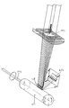
- the roller-shaped (cylindrical) target 1 (which can consist of more than one cylindrical section made of a different material in each case) is fastened to a holder 2 so as to be rotatable about the cylinder axis and displaceable along this axis.
- the laser beams are focused on the cylinder wall to form a line 4 running parallel to the cylinder axis by means of a cylindrical lens 3. Material is removed from the target and deposited on a substrate 5.
- the point of impact of line 4 lies below the connecting line between the center of the cylindrical lens and the central axis of the target. In this way it is achieved that the plasma is formed in the direction of the substrate 4, whereby the formation of the layer to be deposited on the substrate is favored.
- An arrangement of the type described was used to produce thin layers of material from an oxidic high-temperature superconductor made of YBa2Cu3O7, a pulsed excimer laser (LAMBDA PHYSIK, EMG 201) being used.
- LAMBDA PHYSIK pulsed excimer laser
Landscapes
- Chemical & Material Sciences (AREA)
- Engineering & Computer Science (AREA)
- Mechanical Engineering (AREA)
- Chemical Kinetics & Catalysis (AREA)
- Materials Engineering (AREA)
- Metallurgy (AREA)
- Organic Chemistry (AREA)
- Toxicology (AREA)
- Health & Medical Sciences (AREA)
- Physics & Mathematics (AREA)
- Optics & Photonics (AREA)
- Manufacturing & Machinery (AREA)
- Physical Vapour Deposition (AREA)
- Inorganic Compounds Of Heavy Metals (AREA)
Description
- Die Erfindung bezieht sich auf eine Anordnung zum Abtragen von Material eines Targets, bestehend aus dem Target und einem drehbaren Halter für das Target, auf welches die Strahlen eines Lasers zum Abdampfen des Targetmaterials gerichtet sind.
- Eine derartige Anordnung ist beispielsweise in der Patentanmeldung DE-A-38 22 502 (P 38 22 502.6-45) beschrieben. Sie ist in einer UHV-Kammer angeordnet und dient zur Erzielung stöchiometrischer Abbildungen des Targets, d. h. zur Beschichtung von Substraten in der exakten Zusammensetzung des Targetmaterials, wobei durch die Abtragung von Targetmaterial in der UHV-Kammer ein Plasma aus dem Targetmaterial erzeugt wird. Es wird ein Excimerlaser gepulst verwendet, dessen rechteckiges Strahlprofil mit Hilfe einer Zylinderlinse zu einem Strich fokussiert wird. Damit werden hohe Abscheidungsraten bei gleichzeitig stöchiometrischer Abbildung erreicht. Das Target wird dabei gedreht und die Laserstrahlen auf die Stirnfläche des plattenförmigen Targets gerichtet. Dadurch wird zwar eine zunächst homogene Abtragung erzielt, jedoch kommt es zu einer Kraterbildung in der Targetmitte, die einerseits die Standzeit des Targets verringert, andererseits die Homogenität und Reproduzierbarkeit des Prozesses beeinträchtigt.
- Es ist daher Aufgabe der Erfindung, eine Anordnung der eingangs bezeichneten Art zu schaffen, bei der die angegebenen Nachteile nicht auftreten.
- Diese Aufgabe wird durch eine Anordnung mit den Merkmalen des Anspruchs 1 gelöst.
- Bei der erfindungsgemäßen Anordnung wird ein zylinderförmiges bzw. walzenförmiges Target eingesetzt, das zweckmäßigerweise nicht nur um die Zylinderachse drehbar, sondern um diese Achse auch verschiebbar angeordnet ist. Das Abtragen des Targetmaterials erfolgt durch Laserstrahlen, die so fokussiert sind, daß sie in einer Linie auf den Zylindermantel auftreffen. Hierdurch wird eine gleichmäßige Ablation ohne die oben genannten Nachteile erzielt. Zur guten Ausnutzung der Anordnung wird der Laser so ausgerichtet, daß die Linie praktisch parallel zur Zylinderachse verläuft.
- Bei Verfahren zur Beschichtung von Substraten hat sich gezeigt, daß die optimale Ausbildung des Plasmas in Richtung auf das zu beschichtende Substrat von dem Einfallswinkel der Strahlen auf das Target und der Lage der Auftreffstelle (der Lage der Linie auf dem Zylindermantel) abhängt. Eine entsprechende Justage der Anordnung kann dabei durch Ausrichtung der Laserstrahlen, aber auch durch seitliche Verschiebung des Targets vorgenommen werden. Es ist daher zweckmäßig, daß das Target zusätzlich seitlich verschiebbar ist. Die seitliche Verschiebung (längs der Achse des zylindrischen Targets) ergibt die Möglichkeit, bei Targets, die aus mehr als einem zylindrischen Teilstück aus jeweils unterschiedlichem Material bestehen, Mehrfachschichten herzustellen, ohne die Apparatur öffnen und das Target auswechseln zu müssen.
- In der Zeichnung ist eine Ausführungsform der Anordnung schematisch dargestellt und wird im folgenden näher erläutert.
- Das walzen- (zylinder-)förmige Target 1 (das aus mehr als einem zylindrischen Teilstück aus jeweils anderem Material bestehen kann) ist an einem Halter 2 drehbar um die Zylinderachse und längs dieser Achse verschiebbar befestigt. Mittels einer Zylinderlinse 3 werden die Laserstrahlen zu einer parallel zur Zylinderachse verlaufenden Linie 4 auf die Zylinderwandung fokussiert. Dabei wird Material vom Target abgetragen und auf einem Substrat 5 abgeschieden.
- Wie aus der Zeichnung hervorgeht, liegt die Auftreffstelle der Linie 4 unterhalb der Verbindungslinie zwischen der Mitte der Zylinderlinse und der Mittelachse des Targets. Auf diese Weise wird erreicht, daß das Plasma sich in Richtung des Substrats 4 ausbildet, wodurch die Bildung der auf dem Substrat abzuscheidenden Schicht begünstigt ist.
- Eine Anordnung der beschriebenen Art wurde eingesetzt zur Herstellung dünner Schichten aus Material eines oxydischen Hochtemperatur-Supraleiters aus YBa₂Cu₃O₇, wobei ein gepulster Excimerlaser (LAMBDA PHYSIK, EMG 201) eingesetzt wurde.
Claims (5)
- Anordnung zum Abtragen von Material eines Targets, bestehend aus dem Target und einem drehbaren Halter für das Target, auf welches die Strahlen eines Lasers zum Abdampfen des Targetmaterials gerichtet sind,
dadurch gekennzeichnet,
daß das Target (1) zylinderförmig ist und mittels des Halters (2) um die Zylinderachse drehbar ist und die Strahlen des Lasers auf den Zylindermantel gerichtet sind. - Anordnung nach Anspruch 1,
dadurch gekennzeichnet,
daß das Target (1) längs der Zylinderachse verschiebbar ist. - Anordnung nach Anspruch 1 oder 2,
dadurch gekennzeichnet,
daß die Laserstrahlen so fokussiert sind, daß sie in einer Linie (4) auf den Zylindermantel auftreffen. - Anordnung nach Anspruch 3,
dadurch gekennzeichnet,
daß die Linie (4) parallel zur Zylinderachse verläuft. - Anordnung nach einem der vorangehenden Ansprüche,
dadurch gekennzeichnet,
daß das Target (1) seitlich verschiebbar ist.
Applications Claiming Priority (2)
| Application Number | Priority Date | Filing Date | Title |
|---|---|---|---|
| DE3914476A DE3914476C1 (de) | 1989-05-02 | 1989-05-02 | |
| DE3914476 | 1989-05-02 |
Publications (2)
| Publication Number | Publication Date |
|---|---|
| EP0396099A1 EP0396099A1 (de) | 1990-11-07 |
| EP0396099B1 true EP0396099B1 (de) | 1994-10-12 |
Family
ID=6379930
Family Applications (1)
| Application Number | Title | Priority Date | Filing Date |
|---|---|---|---|
| EP90108262A Expired - Lifetime EP0396099B1 (de) | 1989-05-02 | 1990-04-30 | Anordnung zum Abtragen von Material eines Targets |
Country Status (4)
| Country | Link |
|---|---|
| US (1) | US5084300A (de) |
| EP (1) | EP0396099B1 (de) |
| JP (1) | JPH0356670A (de) |
| DE (2) | DE3914476C1 (de) |
Families Citing this family (28)
| Publication number | Priority date | Publication date | Assignee | Title |
|---|---|---|---|---|
| US6149988A (en) * | 1986-09-26 | 2000-11-21 | Semiconductor Energy Laboratory Co., Ltd. | Method and system of laser processing |
| US5708252A (en) * | 1986-09-26 | 1998-01-13 | Semiconductor Energy Laboratory Co., Ltd. | Excimer laser scanning system |
| US5200230A (en) * | 1987-06-29 | 1993-04-06 | Dunfries Investments Limited | Laser coating process |
| US6261856B1 (en) | 1987-09-16 | 2001-07-17 | Semiconductor Energy Laboratory Co., Ltd. | Method and system of laser processing |
| US5578350A (en) * | 1990-07-03 | 1996-11-26 | Fraunhofer-Gesellschaft | Method for depositing a thin layer on a substrate by laser pulse vapor deposition |
| EP0489889B1 (de) * | 1990-07-03 | 1994-11-02 | Fraunhofer-Gesellschaft Zur Förderung Der Angewandten Forschung E.V. | Verfahren zur abscheidung dünner schichten mittels laserimpuls-gasphasenabscheidung (lpvd) |
| DE4022817C1 (de) * | 1990-07-18 | 1991-11-07 | Deutsche Forschungsanstalt Fuer Luft- Und Raumfahrt Ev, 5300 Bonn, De | |
| JPH0532494A (ja) * | 1991-07-29 | 1993-02-09 | Sumitomo Electric Ind Ltd | 複合酸化物超電導薄膜の成膜方法 |
| US5242706A (en) * | 1991-07-31 | 1993-09-07 | The United States Of America As Represented By The Secretary Of The Navy | Laser-deposited biocompatible films and methods and apparatuses for producing same |
| US5227204A (en) * | 1991-08-27 | 1993-07-13 | Northeastern University | Fabrication of ferrite films using laser deposition |
| DE4229399C2 (de) * | 1992-09-03 | 1999-05-27 | Deutsch Zentr Luft & Raumfahrt | Verfahren und Vorrichtung zum Herstellen einer Funktionsstruktur eines Halbleiterbauelements |
| JP3255469B2 (ja) * | 1992-11-30 | 2002-02-12 | 三菱電機株式会社 | レーザ薄膜形成装置 |
| GB2300426B (en) * | 1992-11-30 | 1997-05-28 | Mitsubishi Electric Corp | Thin film forming apparatus using laser |
| US5405659A (en) * | 1993-03-05 | 1995-04-11 | University Of Puerto Rico | Method and apparatus for removing material from a target by use of a ring-shaped elliptical laser beam and depositing the material onto a substrate |
| US5432313A (en) * | 1993-06-23 | 1995-07-11 | The United States Of America As Represented By The Secretary Of The Army | Target configurations for increasing the size of films prepared by laser ablation |
| US5411772A (en) * | 1994-01-25 | 1995-05-02 | Rockwell International Corporation | Method of laser ablation for uniform thin film deposition |
| DE4405598C1 (de) * | 1994-02-22 | 1995-09-21 | Deutsche Forsch Luft Raumfahrt | Verfahren zum Beschichten und Beschichtungsvorrichtung |
| AU4194896A (en) * | 1994-10-18 | 1996-05-06 | Edsi, Inc. | Apparatus for depositing a layer of material on a substrate |
| AT402945B (de) * | 1995-07-03 | 1997-09-25 | Joanneum Research Forschungsge | Verfahren und vorrichtung zur beschichtung der oberfläche eines substrats |
| AUPR026100A0 (en) * | 2000-09-20 | 2000-10-12 | Tamanyan, Astghik | Deposition of thin films by laser ablation |
| DE10248962B4 (de) * | 2002-10-21 | 2007-10-25 | THEVA DüNNSCHICHTTECHNIK GMBH | Verfahren zur Herstellung einer Hochtemperatur-Supraleiterschicht |
| JP2005089793A (ja) * | 2003-09-16 | 2005-04-07 | Sumitomo Electric Ind Ltd | 薄膜の製造方法ならびに薄膜線材の製造方法およびパルスレーザ蒸着装置 |
| WO2006017510A2 (en) * | 2004-08-02 | 2006-02-16 | J.P. Sercel Associates, Inc. | System and method for laser machining |
| GB2419894B (en) * | 2004-10-22 | 2009-08-26 | Plasma Quest Ltd | Sputtering system |
| ATE537277T1 (de) * | 2008-08-25 | 2011-12-15 | Solmates Bv | Verfahren zur abscheidung eines materials |
| EP2910664B1 (de) * | 2014-02-21 | 2019-04-03 | Solmates B.V. | Vorrichtung zur abscheidung eines materials durch gepulste laserabscheidung sowie gepulstes laserverfahren zur abscheidung eines materials mit der vorrichtung |
| FI20155578A (fi) * | 2015-08-10 | 2017-02-11 | Picodeon Ltd Oy | Menetelmä ohutkalvojen valmistamiseksi laserablaatiolla käyttämällä moniosaisia laserpulsseja rengasmaisen pyörivän kohtion kanssa |
| JP2025537560A (ja) * | 2023-10-11 | 2025-11-18 | マル エルアンドシー カンパニー リミテッド | パルスレーザ蒸着による超電導層薄膜蒸着装置 |
Family Cites Families (16)
| Publication number | Priority date | Publication date | Assignee | Title |
|---|---|---|---|---|
| US3538298A (en) * | 1968-07-17 | 1970-11-03 | Gen Electric | Method for balancing rotating objects with laser radiation |
| US4065656A (en) * | 1975-06-30 | 1977-12-27 | Corning Glass Works | Electrical resistor and method of production |
| US4200382A (en) * | 1978-08-30 | 1980-04-29 | Polaroid Corporation | Photographic processing roller and a novel method which utilizes a pulsed laser for manufacturing the roller |
| US4304978A (en) * | 1978-10-05 | 1981-12-08 | Coherent, Inc. | Heat treating using a laser |
| US4281030A (en) * | 1980-05-12 | 1981-07-28 | Bell Telephone Laboratories, Incorporated | Implantation of vaporized material on melted substrates |
| US4701592A (en) * | 1980-11-17 | 1987-10-20 | Rockwell International Corporation | Laser assisted deposition and annealing |
| JPS58130443A (ja) * | 1982-01-28 | 1983-08-03 | Fuji Photo Film Co Ltd | 磁気記録媒体の製造方法 |
| US4427723A (en) * | 1982-02-10 | 1984-01-24 | Rockwell International Corporation | Method and apparatus for laser-stimulated vacuum deposition and annealing technique |
| US4566936A (en) * | 1984-11-05 | 1986-01-28 | North American Philips Corporation | Method of trimming precision resistors |
| US4756811A (en) * | 1985-09-30 | 1988-07-12 | Kabushiki Kaisha Toshiba | Method for manufacturing bubble-mode optical recording media |
| US4816293A (en) * | 1986-03-27 | 1989-03-28 | Mitsubishi Denki Kabushiki Kaisha | Process for coating a workpiece with a ceramic material |
| GB2208390B (en) * | 1987-08-06 | 1991-03-27 | Plessey Co Plc | Thin film deposition process |
| US4874741A (en) * | 1988-04-14 | 1989-10-17 | The Research Foundation Of State University Of New York | Non-enhanced laser evaporation of oxide superconductors |
| DE3822502C1 (de) * | 1988-07-03 | 1989-08-24 | Kernforschungsanlage Juelich Gmbh, 5170 Juelich, De | |
| US5015492A (en) * | 1989-04-03 | 1991-05-14 | Rutgers University | Method and apparatus for pulsed energy induced vapor deposition of thin films |
| US5019552A (en) * | 1990-02-20 | 1991-05-28 | The United States Of America As Represented By The United States Department Of Energy | Long-laser-pulse method of producing thin films |
-
1989
- 1989-05-02 DE DE3914476A patent/DE3914476C1/de not_active Expired - Lifetime
-
1990
- 1990-04-27 JP JP2110708A patent/JPH0356670A/ja active Pending
- 1990-04-30 EP EP90108262A patent/EP0396099B1/de not_active Expired - Lifetime
- 1990-04-30 DE DE59007423T patent/DE59007423D1/de not_active Expired - Fee Related
- 1990-05-02 US US07/517,635 patent/US5084300A/en not_active Expired - Fee Related
Non-Patent Citations (1)
| Title |
|---|
| Zeitschrift für Metallkunde 75 (1984) November Nr. 11 Stuttgart, Duetschland, Seiten 847-854 ; J. A. Thornton: "Hollow Cathode Magnetron Sputtering of Metallurgical Coatings" * |
Also Published As
| Publication number | Publication date |
|---|---|
| EP0396099A1 (de) | 1990-11-07 |
| US5084300A (en) | 1992-01-28 |
| JPH0356670A (ja) | 1991-03-12 |
| DE3914476C1 (de) | 1990-06-21 |
| DE59007423D1 (de) | 1994-11-17 |
Similar Documents
| Publication | Publication Date | Title |
|---|---|---|
| EP0396099B1 (de) | Anordnung zum Abtragen von Material eines Targets | |
| EP0285745B1 (de) | Verfahren und Vorrichtungen zum Vakuumbeschichten mittels einer elektrischen Bogenentladung | |
| DE4126236C2 (de) | Rotierende Magnetron-Kathode und Verwendung einer rotierenden Magnetron-Kathode | |
| EP1537057B1 (de) | Verfahren zur herstellung von schichten und schichtsystemen sowie beschichtetes substrat | |
| DE69904517T2 (de) | Verfahren und Vorrichtung zur dreidimensionalen Verarbeitung von strangförmigen Substraten | |
| DE68905286T2 (de) | Verfahren und vorrichtung zur herstellung oder modifikation von schneidkanten. | |
| DE69506338T2 (de) | Verfahren und Gerät zur Herstellung von supraleitenden Komponenten via Laserablation, gefolgt durch Laserbearbeitung | |
| DE3815006A1 (de) | Vorrichtung zum herstellen von beschichtungen mit abgestufter zusammensetzung | |
| EP0535019A1 (de) | Verfahren und vorrichtung zum beschichten von substratmaterial. | |
| EP0165565A2 (de) | Vakuum-Plasma-Beschichtungsanlage | |
| DE3854307T2 (de) | Hohlkathodenkanone und Vorrichtung zur Materialablagerung durch Ionenbeschichtung. | |
| EP1626433B1 (de) | Magnetronsputtereinrichtung, Zylinderkathode und Verfahren zur Aufbringung von dünnen Mehrkomponentenschichten auf einem Substrat | |
| DE3914986A1 (de) | Beschichtungsverfahren zum schutz von keramikgegenstaenden gegen mechanische und thermische stoereinfluesse und schutzbeschichteter keramikgegenstand | |
| DE69316111T2 (de) | Topografische, selektive Muster | |
| DE2812285C2 (de) | Verfahren zum Verdampfen von Legierungsschmelzen aus Metallen mit voneinander abweichenden Dampfdrücken | |
| DE102019200681B4 (de) | Schneidwerkzeug mit amorphem Kohlenstoff und Multilagenbeschichtung und Verfahren zu dessen Herstellung | |
| DE4203371C1 (de) | ||
| DE10393678B4 (de) | Verfahren zum Bilden einer Schicht auf einem Substrat | |
| DE69310039T2 (de) | Verfahren und Vorrichtung zum Vorbehandeln und Beschichten einer Oberfläche | |
| DE3925085C1 (de) | ||
| DE202016004006U1 (de) | Materialbearbeitungssystem | |
| DE4405598C1 (de) | Verfahren zum Beschichten und Beschichtungsvorrichtung | |
| DE3418332C2 (de) | ||
| DE10239163A1 (de) | Vorrichtung und Verfahren zur Ausbildung von Gradientenschichten auf Substraten in einer Vakuumkammer | |
| EP0806491B1 (de) | Verfahren zum Aufdampfen von Vergütungsschichten auf optische Substrate |
Legal Events
| Date | Code | Title | Description |
|---|---|---|---|
| PUAI | Public reference made under article 153(3) epc to a published international application that has entered the european phase |
Free format text: ORIGINAL CODE: 0009012 |
|
| AK | Designated contracting states |
Kind code of ref document: A1 Designated state(s): CH DE FR GB IT LI NL |
|
| 17P | Request for examination filed |
Effective date: 19901127 |
|
| 17Q | First examination report despatched |
Effective date: 19930129 |
|
| GRAA | (expected) grant |
Free format text: ORIGINAL CODE: 0009210 |
|
| AK | Designated contracting states |
Kind code of ref document: B1 Designated state(s): CH DE FR GB IT LI NL |
|
| REF | Corresponds to: |
Ref document number: 59007423 Country of ref document: DE Date of ref document: 19941117 |
|
| GBT | Gb: translation of ep patent filed (gb section 77(6)(a)/1977) |
Effective date: 19941205 |
|
| ITF | It: translation for a ep patent filed | ||
| ET | Fr: translation filed | ||
| PLBE | No opposition filed within time limit |
Free format text: ORIGINAL CODE: 0009261 |
|
| STAA | Information on the status of an ep patent application or granted ep patent |
Free format text: STATUS: NO OPPOSITION FILED WITHIN TIME LIMIT |
|
| 26N | No opposition filed | ||
| REG | Reference to a national code |
Ref country code: GB Ref legal event code: IF02 |
|
| PGFP | Annual fee paid to national office [announced via postgrant information from national office to epo] |
Ref country code: DE Payment date: 20050408 Year of fee payment: 16 |
|
| PGFP | Annual fee paid to national office [announced via postgrant information from national office to epo] |
Ref country code: NL Payment date: 20050418 Year of fee payment: 16 |
|
| PGFP | Annual fee paid to national office [announced via postgrant information from national office to epo] |
Ref country code: GB Payment date: 20050419 Year of fee payment: 16 Ref country code: FR Payment date: 20050419 Year of fee payment: 16 |
|
| PGFP | Annual fee paid to national office [announced via postgrant information from national office to epo] |
Ref country code: CH Payment date: 20050422 Year of fee payment: 16 |
|
| PG25 | Lapsed in a contracting state [announced via postgrant information from national office to epo] |
Ref country code: LI Free format text: LAPSE BECAUSE OF NON-PAYMENT OF DUE FEES Effective date: 20060430 Ref country code: GB Free format text: LAPSE BECAUSE OF NON-PAYMENT OF DUE FEES Effective date: 20060430 Ref country code: CH Free format text: LAPSE BECAUSE OF NON-PAYMENT OF DUE FEES Effective date: 20060430 |
|
| PGFP | Annual fee paid to national office [announced via postgrant information from national office to epo] |
Ref country code: IT Payment date: 20060430 Year of fee payment: 17 |
|
| PG25 | Lapsed in a contracting state [announced via postgrant information from national office to epo] |
Ref country code: NL Free format text: LAPSE BECAUSE OF NON-PAYMENT OF DUE FEES Effective date: 20061101 Ref country code: DE Free format text: LAPSE BECAUSE OF NON-PAYMENT OF DUE FEES Effective date: 20061101 |
|
| REG | Reference to a national code |
Ref country code: CH Ref legal event code: PL |
|
| GBPC | Gb: european patent ceased through non-payment of renewal fee |
Effective date: 20060430 |
|
| NLV4 | Nl: lapsed or anulled due to non-payment of the annual fee |
Effective date: 20061101 |
|
| REG | Reference to a national code |
Ref country code: FR Ref legal event code: ST Effective date: 20061230 |
|
| PG25 | Lapsed in a contracting state [announced via postgrant information from national office to epo] |
Ref country code: FR Free format text: LAPSE BECAUSE OF NON-PAYMENT OF DUE FEES Effective date: 20060502 |
|
| PG25 | Lapsed in a contracting state [announced via postgrant information from national office to epo] |
Ref country code: IT Free format text: LAPSE BECAUSE OF NON-PAYMENT OF DUE FEES Effective date: 20070430 |