EP0397965A2 - Anzeigevorrichtung - Google Patents
Anzeigevorrichtung Download PDFInfo
- Publication number
- EP0397965A2 EP0397965A2 EP90101853A EP90101853A EP0397965A2 EP 0397965 A2 EP0397965 A2 EP 0397965A2 EP 90101853 A EP90101853 A EP 90101853A EP 90101853 A EP90101853 A EP 90101853A EP 0397965 A2 EP0397965 A2 EP 0397965A2
- Authority
- EP
- European Patent Office
- Prior art keywords
- light emitting
- emitting pixels
- display
- display apparatus
- arrangement
- Prior art date
- Legal status (The legal status is an assumption and is not a legal conclusion. Google has not performed a legal analysis and makes no representation as to the accuracy of the status listed.)
- Granted
Links
Images


Classifications
-
- H—ELECTRICITY
- H04—ELECTRIC COMMUNICATION TECHNIQUE
- H04N—PICTORIAL COMMUNICATION, e.g. TELEVISION
- H04N9/00—Details of colour television systems
- H04N9/12—Picture reproducers
- H04N9/30—Picture reproducers using solid-state colour display devices
-
- H—ELECTRICITY
- H04—ELECTRIC COMMUNICATION TECHNIQUE
- H04N—PICTORIAL COMMUNICATION, e.g. TELEVISION
- H04N9/00—Details of colour television systems
- H04N9/12—Picture reproducers
Definitions
- the present invention relates to a display apparatus, particularly a color display apparatus of a large screen, comprising a large number of display devices each having a plurality of light emitting pixels arranged in the form of a matrix.
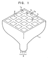
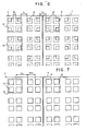
- Fig. 1 is a perspective view showing a display device used in a conventional display apparatus such as that described, for example, in Japanese Utility Model Laid-Open No. 12258/87.
- the reference numeral 1 denotes a display device
- numeral 2 denotes each of plural light emitting pixels 2 being arranged in a matrix form on the display surface of the display device 1
- numeral 3 denotes each of control electrodes for driving the light emitting pixels 2.
- the reference mark T1 represents a spacing between adjacent light emitting pixels 2
- T2 represents a spacing between the marginal portion of the display device 1 and the light emitting pixels 2, the spacing T2 corresponding to the thickness of each side wall of the vessel which form the display device 1.
- Fig. 2 shows an example of a display portion screen of the display apparatus composed of the display devices 1 in a large number.
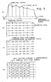
- Fig. 3 shows the relation between sampling a television signal and displaying it.
- an appropriate space T1 is required between adjacent light emitting pixels 2 of the display device 1. This is because of the premise that a large screen display is to be constituted by arranging a large number of the display devices 1 as shown in Fig. 2.
- the space T1 is twice or larger the wall thickness T2 of the marginal portion of each display device 1. Consequently, on the screen as the display portion there are arranged a large number of the light emitting pixels 2 at equal intervals.
- Fig. 3 shows the relation between television signal processing and display
- Fig. 3(a) shows a television signal of 1H
- Fig. 3(b) shows how the television signal is sampled at a predetermined certain interval of time.
- Figs. 3(c) and (d) show the relation between sampled signal data at sampling points 01, 02, 03, ... on scanning lines 0, 1, 2, 3, ... and the arranged light emitting pixels 2, in which the television signal sampling rate is constant in correspondence to the light emitting pixels 2 which are arranged at equal pitches.
- the luminance in the emission of light of each light emitting pixel 2 is controlled so as to be proportional to the amplitude of the television signal.
- the light emitting pixels 2 are arranged discretely at predetermined intervals, when seen from an appropriate distance, they can be recognized as a continuous television picture.
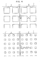
- Fig. 4 shows an example of how to attain a higher resolution.
- Fig. 4(a) shows a joint portion between conventional display devices 1
- Fig. 4(b) shows a joint portion between display devices 1 each having four-fold density of light emitting pixels 2 to increase the resolution. Since it is difficult to decrease the wall thickness T2 of each display device 1, there provokes a great conflict between keeping the picture element pitch equal in the joint portion of two display devices 1 and making the space T1 between adjacent light emitting pixels 2 small.
- the conventional display apparatus Since the conventional display apparatus is constructed as above, the light emission area of each light emitting pixel becomes smaller with increase in density of the light emitting pixels when pursuing a higher resolution of display, as can be seen also from Fig. 4. This results in emphasizing the discontinuance of a discrete arrangement of picture elements, causing roughness of a television picture when displayed, thus leading to deterioration of the picture quality. Further, the surface luminance of the display screen becomes lower.
- the present invention has been accomplished for overcoming the above-mentioned problems and it is an object thereof to provide a display apparatus in which some consideration is given to the arrangement of picture elements on each display device, thereby permitting the display of a smooth and high luminance picture at a high resolution and with less roughness on a screen while maintaining the conventional simple way of signal processing.
- each two, three or four light emitting pixels adjacent to one another in the row and/or column direction on a display screen are arranged in groups so that the intragroup arrangement pitch, P0, of the light emitting pixels in each group is smaller than the intergroup arrangement pitch P1, of adjacent groups, and yet the light emitting pixels are operated on the basis of television signal data sampled at predetermined certain intervals of time.
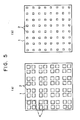
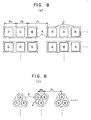
- Fig. 5(a) shows, for example, an arrangement of picture elements in a display device 1 for high resolution display used in a display apparatus according to an embodiment of the present invention
- Fig. 5(b) shows a picture element arrangement according to the prior art for a purpose of comparison.
- four light emitting pixels 2 adjacent to one another in the row and column directions are made one group as indicated by the reference numeral 4 and the area of each light emitting pixel 2 in each group 4 is increased.
- Fig. 6 shows how to enlarge the area of each light emitting pixel 2.
- a space T1 almost equal to a space T3 in the joint portion of the display devices 1 has heretofore been provided between light emitting pixels 2 indicated with solid lines, while in the present invention it is provided between adjacent groups 4 of light emitting pixels 2.
- the area of each picture element 2 is enlarged as indicated with broken lines by reducing the space T4 between adjacent light emitting pixels 2 in each group 4 smaller than the space T1.
- the condition that the light emitting pixels 2 should be arranged in equal pitches as in the prior art is no longer satisfied. More particularly, in the conventional signal processing, sampling is performed with a certain period in correspondence to an equal pitch arrangement of the light emitting pixels 2, but in order to reproduce a television picture exactly and in the case of an unequal pitch arrangement of the light emitting pixels 2 as in the present invention, it becomes necessary to change the sampling period accordingly. It is possible to change the sampling period in the horizontal direction, but in the vertical direction the television signal itself is sampled by scanning lines and is in the form of a discrete signal at a certain period, so it is not easy to change that period.
- the present invention premises sampling with a certain period which can be easily realized technically. And studies were made synthetically about the trade-off between the following two points occurring under the above premise.
- the increase of the light emission area is effective in diminishing the roughness of display, obtaining a high quality picture in a display apparatus in which picture elements are arranged discretely as shown, for example, in Japanese Patent Laid-Open No. 2086/89. Further, as is apparent also from Fig. 5(a), with increase in the light emission area of the light emitting pixels 2, it is possible to attain a high luminance of display easily.
- each light emitting pixel 2 As shown in Fig. 8, there are, for example, several kinds of color schemes of the light emitting pixels 2, and the present invention is effective in all of them.
- two, three or four adjacent light emitting pixels in the row and/or column direction in the display portion are made one group and the intragroup arrangement pitch of the light emitting pixels in each group is made shorter than the intergroup arrangement pitch of adjacent groups, further, each of the light emitting pixels are operated individually on the basis of television signal data sampled with a certain period. Consequently, there is obtained a smooth, roughness-free display of extremely high luminance and quality.
Landscapes
- Engineering & Computer Science (AREA)
- Multimedia (AREA)
- Signal Processing (AREA)
- Transforming Electric Information Into Light Information (AREA)
- Devices For Indicating Variable Information By Combining Individual Elements (AREA)
- Control Of Indicators Other Than Cathode Ray Tubes (AREA)
- Cathode-Ray Tubes And Fluorescent Screens For Display (AREA)
- Video Image Reproduction Devices For Color Tv Systems (AREA)
Applications Claiming Priority (2)
| Application Number | Priority Date | Filing Date | Title |
|---|---|---|---|
| JP1124008A JPH0817086B2 (ja) | 1989-05-17 | 1989-05-17 | 表示装置 |
| JP124008/89 | 1989-05-17 |
Publications (3)
| Publication Number | Publication Date |
|---|---|
| EP0397965A2 true EP0397965A2 (de) | 1990-11-22 |
| EP0397965A3 EP0397965A3 (de) | 1992-10-21 |
| EP0397965B1 EP0397965B1 (de) | 1997-05-14 |
Family
ID=14874747
Family Applications (1)
| Application Number | Title | Priority Date | Filing Date |
|---|---|---|---|
| EP90101853A Expired - Lifetime EP0397965B1 (de) | 1989-05-17 | 1990-01-31 | Anzeigevorrichtung |
Country Status (5)
| Country | Link |
|---|---|
| US (1) | US5767837A (de) |
| EP (1) | EP0397965B1 (de) |
| JP (1) | JPH0817086B2 (de) |
| AU (1) | AU612536B2 (de) |
| SG (1) | SG68565A1 (de) |
Cited By (2)
| Publication number | Priority date | Publication date | Assignee | Title |
|---|---|---|---|---|
| FR2687494A1 (fr) * | 1992-02-18 | 1993-08-20 | Thomson Tubes Electroniques | Ecran matriciel notamment de grandes dimensions et procede pour la realisation d'un tel ecran matriciel. |
| US6243060B1 (en) | 1997-02-20 | 2001-06-05 | Sony Corporation | Image display and its pixel arrangement method |
Families Citing this family (59)
| Publication number | Priority date | Publication date | Assignee | Title |
|---|---|---|---|---|
| US5122733A (en) * | 1986-01-15 | 1992-06-16 | Karel Havel | Variable color digital multimeter |
| JPH09319332A (ja) * | 1996-05-27 | 1997-12-12 | Matsushita Electric Ind Co Ltd | Led表示装置およびled表示方法 |
| JP3215913B2 (ja) * | 1997-07-30 | 2001-10-09 | 富士通株式会社 | 液晶表示装置の表示制御方法及び液晶表示装置 |
| US7215347B2 (en) * | 1997-09-13 | 2007-05-08 | Gia Chuong Phan | Dynamic pixel resolution, brightness and contrast for displays using spatial elements |
| US20040085277A1 (en) * | 1998-04-10 | 2004-05-06 | Fuji Photo Film Co., Ltd. | Monochromatic image display system |
| JPH11338423A (ja) * | 1998-05-15 | 1999-12-10 | Internatl Business Mach Corp <Ibm> | カラー表示方法、この表示方法に適するマトリックス駆動用液晶表示モジュール、及び、この液晶表示モジュールを含むpcシステム、並びに、プロジェクションタイプ表示装置 |
| US6278434B1 (en) | 1998-10-07 | 2001-08-21 | Microsoft Corporation | Non-square scaling of image data to be mapped to pixel sub-components |
| US6188385B1 (en) | 1998-10-07 | 2001-02-13 | Microsoft Corporation | Method and apparatus for displaying images such as text |
| US6236390B1 (en) | 1998-10-07 | 2001-05-22 | Microsoft Corporation | Methods and apparatus for positioning displayed characters |
| ATE511688T1 (de) * | 1998-10-07 | 2011-06-15 | Microsoft Corp | Zuordnung von bilddatenproben zu bildpunkt- teilkomponenten auf einer, in streifen aufgeteilten anzeigevorrichtung |
| US6597360B1 (en) | 1998-10-07 | 2003-07-22 | Microsoft Corporation | Automatic optimization of the position of stems of text characters |
| US6307566B1 (en) | 1998-10-07 | 2001-10-23 | Microsoft Corporation | Methods and apparatus for performing image rendering and rasterization operations |
| US6356278B1 (en) | 1998-10-07 | 2002-03-12 | Microsoft Corporation | Methods and systems for asymmeteric supersampling rasterization of image data |
| ATE534986T1 (de) | 1998-10-07 | 2011-12-15 | Microsoft Corp | Abbildung von vordergrund/hintergrund farbbildaten mit pixelteilkomponenten |
| US6393145B2 (en) | 1999-01-12 | 2002-05-21 | Microsoft Corporation | Methods apparatus and data structures for enhancing the resolution of images to be rendered on patterned display devices |
| US6973210B1 (en) | 1999-01-12 | 2005-12-06 | Microsoft Corporation | Filtering image data to obtain samples mapped to pixel sub-components of a display device |
| JP2000214825A (ja) * | 1999-01-20 | 2000-08-04 | Nec Corp | バックライト表示装置及び方法 |
| US7134091B2 (en) * | 1999-02-01 | 2006-11-07 | Microsoft Corporation | Quality of displayed images with user preference information |
| US6624828B1 (en) | 1999-02-01 | 2003-09-23 | Microsoft Corporation | Method and apparatus for improving the quality of displayed images through the use of user reference information |
| US6750875B1 (en) | 1999-02-01 | 2004-06-15 | Microsoft Corporation | Compression of image data associated with two-dimensional arrays of pixel sub-components |
| US6342896B1 (en) | 1999-03-19 | 2002-01-29 | Microsoft Corporation | Methods and apparatus for efficiently implementing and modifying foreground and background color selections |
| US6342890B1 (en) | 1999-03-19 | 2002-01-29 | Microsoft Corporation | Methods, apparatus, and data structures for accessing sub-pixel data having left side bearing information |
| US6339426B1 (en) | 1999-04-29 | 2002-01-15 | Microsoft Corporation | Methods, apparatus and data structures for overscaling or oversampling character feature information in a system for rendering text on horizontally striped displays |
| JP4912520B2 (ja) * | 1999-05-31 | 2012-04-11 | 三星モバイルディスプレイ株式會社 | マルチディスプレイ装置 |
| US6282327B1 (en) | 1999-07-30 | 2001-08-28 | Microsoft Corporation | Maintaining advance widths of existing characters that have been resolution enhanced |
| US6738526B1 (en) * | 1999-07-30 | 2004-05-18 | Microsoft Corporation | Method and apparatus for filtering and caching data representing images |
| US6226017B1 (en) | 1999-07-30 | 2001-05-01 | Microsoft Corporation | Methods and apparatus for improving read/modify/write operations |
| US6950115B2 (en) | 2001-05-09 | 2005-09-27 | Clairvoyante, Inc. | Color flat panel display sub-pixel arrangements and layouts |
| US7184066B2 (en) * | 2001-05-09 | 2007-02-27 | Clairvoyante, Inc | Methods and systems for sub-pixel rendering with adaptive filtering |
| US7064740B2 (en) * | 2001-11-09 | 2006-06-20 | Sharp Laboratories Of America, Inc. | Backlit display with improved dynamic range |
| US6932477B2 (en) * | 2001-12-21 | 2005-08-23 | Koninklijke Philips Electronics N.V. | Apparatus for providing multi-spectral light for an image projection system |
| US7679614B2 (en) * | 2003-05-06 | 2010-03-16 | Au Optronics Corporation | Matrix driven liquid crystal display module system, apparatus and method |
| US7623105B2 (en) | 2003-11-21 | 2009-11-24 | Sharp Laboratories Of America, Inc. | Liquid crystal display with adaptive color |
| US7164284B2 (en) * | 2003-12-18 | 2007-01-16 | Sharp Laboratories Of America, Inc. | Dynamic gamma for a liquid crystal display |
| US7777714B2 (en) | 2004-05-04 | 2010-08-17 | Sharp Laboratories Of America, Inc. | Liquid crystal display with adaptive width |
| US7532192B2 (en) | 2004-05-04 | 2009-05-12 | Sharp Laboratories Of America, Inc. | Liquid crystal display with filtered black point |
| US7612757B2 (en) | 2004-05-04 | 2009-11-03 | Sharp Laboratories Of America, Inc. | Liquid crystal display with modulated black point |
| US7505018B2 (en) | 2004-05-04 | 2009-03-17 | Sharp Laboratories Of America, Inc. | Liquid crystal display with reduced black level insertion |
| US8395577B2 (en) | 2004-05-04 | 2013-03-12 | Sharp Laboratories Of America, Inc. | Liquid crystal display with illumination control |
| US7602369B2 (en) * | 2004-05-04 | 2009-10-13 | Sharp Laboratories Of America, Inc. | Liquid crystal display with colored backlight |
| US7023451B2 (en) * | 2004-06-14 | 2006-04-04 | Sharp Laboratories Of America, Inc. | System for reducing crosstalk |
| US7556836B2 (en) | 2004-09-03 | 2009-07-07 | Solae, Llc | High protein snack product |
| US7898519B2 (en) | 2005-02-17 | 2011-03-01 | Sharp Laboratories Of America, Inc. | Method for overdriving a backlit display |
| US8050511B2 (en) | 2004-11-16 | 2011-11-01 | Sharp Laboratories Of America, Inc. | High dynamic range images from low dynamic range images |
| US8050512B2 (en) | 2004-11-16 | 2011-11-01 | Sharp Laboratories Of America, Inc. | High dynamic range images from low dynamic range images |
| US7525528B2 (en) | 2004-11-16 | 2009-04-28 | Sharp Laboratories Of America, Inc. | Technique that preserves specular highlights |
| KR101189085B1 (ko) * | 2005-07-14 | 2012-11-09 | 삼성디스플레이 주식회사 | 백라이트 유닛과 이를 포함하는 액정표시장치 |
| US8123375B2 (en) * | 2005-11-18 | 2012-02-28 | Cree, Inc. | Tile for solid state lighting |
| US8121401B2 (en) | 2006-01-24 | 2012-02-21 | Sharp Labortories of America, Inc. | Method for reducing enhancement of artifacts and noise in image color enhancement |
| US9143657B2 (en) | 2006-01-24 | 2015-09-22 | Sharp Laboratories Of America, Inc. | Color enhancement technique using skin color detection |
| EP2035745B1 (de) | 2006-05-31 | 2020-04-29 | IDEAL Industries Lighting LLC | Beleuchtungsvorrichtung mit farbsteuerung und beleuchtungsverfahren |
| US8941580B2 (en) | 2006-11-30 | 2015-01-27 | Sharp Laboratories Of America, Inc. | Liquid crystal display with area adaptive backlight |
| JP4395801B2 (ja) * | 2007-11-13 | 2010-01-13 | ソニー株式会社 | 面状光源装置及び液晶表示装置組立体 |
| US8866410B2 (en) | 2007-11-28 | 2014-10-21 | Cree, Inc. | Solid state lighting devices and methods of manufacturing the same |
| US9013367B2 (en) * | 2008-01-04 | 2015-04-21 | Nanolumens Acquisition Inc. | Flexible display |
| JP5141418B2 (ja) * | 2008-07-24 | 2013-02-13 | セイコーエプソン株式会社 | 画像表示制御装置およびプログラム並びに画像表示制御方法 |
| JP5374306B2 (ja) * | 2009-09-30 | 2013-12-25 | 三菱電機株式会社 | 画像表示装置 |
| US20150016104A1 (en) * | 2013-07-11 | 2015-01-15 | Everlight Electronics Co., Ltd. | Lighting Component And Lighting Device |
| US11719974B2 (en) | 2020-02-03 | 2023-08-08 | Mitsubishi Electric Corporation | Self-luminous body for display apparatus, self-luminous display apparatus, backlight, liquid crystal display apparatus, and method for manufacturing self-luminous body for display apparatus |
Family Cites Families (19)
| Publication number | Priority date | Publication date | Assignee | Title |
|---|---|---|---|---|
| US4326150A (en) * | 1979-03-24 | 1982-04-20 | Mitsubishi Denki Kabushiki Kaisha | Cathode ray tube device for display system |
| US4368485A (en) * | 1981-04-13 | 1983-01-11 | Zenith Radio Corporation | Billboard large screen TV |
| US4661809A (en) * | 1982-05-05 | 1987-04-28 | Litton Systems, Inc. | Magneto-optic chip with gray-scale capability |
| JPS5918347A (ja) * | 1982-07-20 | 1984-01-30 | 松下精工株式会社 | 空気調和機 |
| JPS59151747A (ja) * | 1983-02-18 | 1984-08-30 | Mitsubishi Electric Corp | 陰極線管 |
| CA1239468A (en) * | 1984-01-13 | 1988-07-19 | Yuji Watanabe | Video display system |
| US4723119A (en) * | 1984-05-07 | 1988-02-02 | Futaba Denshi Kogyo Kabushiki Kaisha | Large-sized color display device |
| JPS6164045A (ja) * | 1984-09-04 | 1986-04-02 | Sony Corp | ビ−ムインデツクス型カラ−陰極線管 |
| JPH061674B2 (ja) * | 1984-12-04 | 1994-01-05 | ソニー株式会社 | 螢光表示管 |
| JPS61177078A (ja) * | 1985-01-31 | 1986-08-08 | Sony Corp | 画像表示装置 |
| JPS6212258A (ja) * | 1985-07-09 | 1987-01-21 | Nec Corp | 自動構内交換機の内線キヤンプオン・キヤンセル方式 |
| JPS6275513A (ja) * | 1985-09-30 | 1987-04-07 | Toshiba Electric Equip Corp | 液晶表示装置 |
| US4734779A (en) * | 1986-07-18 | 1988-03-29 | Video Matrix Corporation | Video projection system |
| US4800375A (en) * | 1986-10-24 | 1989-01-24 | Honeywell Inc. | Four color repetitive sequence matrix array for flat panel displays |
| JPS63174377A (ja) * | 1987-01-14 | 1988-07-18 | Mitsubishi Kasei Corp | 光電変換薄膜 |
| JPS642086A (en) * | 1987-06-25 | 1989-01-06 | Mitsubishi Electric Corp | Color display panel |
| EP0324147A3 (de) * | 1988-01-11 | 1990-07-04 | Seiko Epson Corporation | Anzeigeapparat mit Lichtleitern |
| US4924356A (en) * | 1988-12-07 | 1990-05-08 | General Electric Company | Illumination system for a display device |
| JPH02165188A (ja) * | 1988-12-19 | 1990-06-26 | Mitsubishi Electric Corp | 表示素子 |
-
1989
- 1989-05-17 JP JP1124008A patent/JPH0817086B2/ja not_active Expired - Lifetime
-
1990
- 1990-01-22 AU AU48651/90A patent/AU612536B2/en not_active Ceased
- 1990-01-31 SG SG1996005275A patent/SG68565A1/en unknown
- 1990-01-31 EP EP90101853A patent/EP0397965B1/de not_active Expired - Lifetime
-
1993
- 1993-04-16 US US08/047,615 patent/US5767837A/en not_active Expired - Lifetime
Cited By (4)
| Publication number | Priority date | Publication date | Assignee | Title |
|---|---|---|---|---|
| FR2687494A1 (fr) * | 1992-02-18 | 1993-08-20 | Thomson Tubes Electroniques | Ecran matriciel notamment de grandes dimensions et procede pour la realisation d'un tel ecran matriciel. |
| EP0557161A1 (de) * | 1992-02-18 | 1993-08-25 | Thomson Tubes Electroniques | Matrixanzeige, insbesondere von grossen Anzeigeschirmen sowie Herstellungsverfahren für eine solche Matrixanzeige |
| US5369281A (en) * | 1992-02-18 | 1994-11-29 | Thomson Tubes Electroniques | Matrix screen, particularly a large screen, and a method of manufacturing it |
| US6243060B1 (en) | 1997-02-20 | 2001-06-05 | Sony Corporation | Image display and its pixel arrangement method |
Also Published As
| Publication number | Publication date |
|---|---|
| HK1000754A1 (en) | 1998-04-24 |
| US5767837A (en) | 1998-06-16 |
| EP0397965B1 (de) | 1997-05-14 |
| AU612536B2 (en) | 1991-07-11 |
| EP0397965A3 (de) | 1992-10-21 |
| JPH0817086B2 (ja) | 1996-02-21 |
| AU4865190A (en) | 1990-11-22 |
| JPH02304843A (ja) | 1990-12-18 |
| SG68565A1 (en) | 1999-11-16 |
Similar Documents
| Publication | Publication Date | Title |
|---|---|---|
| EP0397965A2 (de) | Anzeigevorrichtung | |
| KR100210822B1 (ko) | 칼라 액정표시장치 | |
| EP0435391B1 (de) | Farbanzeigegerät | |
| EP0777198A1 (de) | Bildverarbeitungsvorrichtung | |
| JPH027089A (ja) | 高解像度フラット・パネル・マトリックス・アレー構造 | |
| KR100247633B1 (ko) | 화소배열구조 및 이를 채용한 액정표시소자 및 그의 구동방법 | |
| CA2106244A1 (en) | Stereoscopic Display Apparatus | |
| EP0911797A3 (de) | Vorrichtung und Steuerungverfahren für eine Flüssigkristallanzeige mit aktiver Matrix | |
| KR100312392B1 (ko) | 디지탈텔레비젼용유니트 | |
| KR19980080468A (ko) | 저밀도 도트 메트릭스 디스플레이에서 고밀도 도트 메트릭스 비트맵 이미지를 디스플레이하는 방법 및 장치 | |
| DE69321279D1 (de) | Anzeigegerät | |
| EP0400992A3 (de) | Verfahren zum Steuern eines Anzeigegeräts | |
| JP3236495B2 (ja) | カラー液晶表示装置 | |
| GB2131217A (en) | Matrix display panel and method of driving the same | |
| JPH0759035A (ja) | ビデオ表示装置 | |
| EP1282105A3 (de) | Verfahren zur Anzeige von Farbbildern | |
| HK1000754B (en) | Display apparatus | |
| CA2164803A1 (en) | Method and Circuit for Driving Picture Display Devices | |
| EP0206518A3 (de) | Vertikaler Raster-Abtastregler | |
| JPH07191630A (ja) | Lcdマルチシンクモニター方法 | |
| ATE171003T1 (de) | Anzeigevorrichtung | |
| EP0884716A3 (de) | Plasmaadressierte Anzeigesystem | |
| JP2535624B2 (ja) | 液晶ディスプレイ装置 | |
| EP0635155B1 (de) | Verfahren zum erzeugen von schattierten farbbildern auf anzeigeschirmen. | |
| JP2000267602A (ja) | Ledユニット |
Legal Events
| Date | Code | Title | Description |
|---|---|---|---|
| PUAI | Public reference made under article 153(3) epc to a published international application that has entered the european phase |
Free format text: ORIGINAL CODE: 0009012 |
|
| AK | Designated contracting states |
Kind code of ref document: A2 Designated state(s): CH FR GB LI |
|
| PUAL | Search report despatched |
Free format text: ORIGINAL CODE: 0009013 |
|
| AK | Designated contracting states |
Kind code of ref document: A3 Designated state(s): CH FR GB LI |
|
| 17P | Request for examination filed |
Effective date: 19930408 |
|
| 17Q | First examination report despatched |
Effective date: 19950208 |
|
| GRAG | Despatch of communication of intention to grant |
Free format text: ORIGINAL CODE: EPIDOS AGRA |
|
| GRAH | Despatch of communication of intention to grant a patent |
Free format text: ORIGINAL CODE: EPIDOS IGRA |
|
| GRAH | Despatch of communication of intention to grant a patent |
Free format text: ORIGINAL CODE: EPIDOS IGRA |
|
| GRAH | Despatch of communication of intention to grant a patent |
Free format text: ORIGINAL CODE: EPIDOS IGRA |
|
| GRAA | (expected) grant |
Free format text: ORIGINAL CODE: 0009210 |
|
| AK | Designated contracting states |
Kind code of ref document: B1 Designated state(s): CH FR GB LI |
|
| REG | Reference to a national code |
Ref country code: CH Ref legal event code: EP Ref country code: CH Ref legal event code: NV Representative=s name: WILLIAM BLANC & CIE CONSEILS EN PROPRIETE INDUSTRI |
|
| ET | Fr: translation filed | ||
| PLBE | No opposition filed within time limit |
Free format text: ORIGINAL CODE: 0009261 |
|
| STAA | Information on the status of an ep patent application or granted ep patent |
Free format text: STATUS: NO OPPOSITION FILED WITHIN TIME LIMIT |
|
| 26N | No opposition filed | ||
| REG | Reference to a national code |
Ref country code: GB Ref legal event code: 746 Effective date: 19990519 |
|
| REG | Reference to a national code |
Ref country code: FR Ref legal event code: D6 |
|
| REG | Reference to a national code |
Ref country code: GB Ref legal event code: IF02 |
|
| PGFP | Annual fee paid to national office [announced via postgrant information from national office to epo] |
Ref country code: CH Payment date: 20050127 Year of fee payment: 16 |
|
| PG25 | Lapsed in a contracting state [announced via postgrant information from national office to epo] |
Ref country code: CH Free format text: LAPSE BECAUSE OF NON-PAYMENT OF DUE FEES Effective date: 20060131 Ref country code: LI Free format text: LAPSE BECAUSE OF NON-PAYMENT OF DUE FEES Effective date: 20060131 |
|
| REG | Reference to a national code |
Ref country code: CH Ref legal event code: PL |
|
| PGFP | Annual fee paid to national office [announced via postgrant information from national office to epo] |
Ref country code: GB Payment date: 20090128 Year of fee payment: 20 |
|
| REG | Reference to a national code |
Ref country code: GB Ref legal event code: PE20 Expiry date: 20100130 |
|
| PG25 | Lapsed in a contracting state [announced via postgrant information from national office to epo] |
Ref country code: GB Free format text: LAPSE BECAUSE OF EXPIRATION OF PROTECTION Effective date: 20100130 |
|
| PGFP | Annual fee paid to national office [announced via postgrant information from national office to epo] |
Ref country code: FR Payment date: 20080830 Year of fee payment: 20 |