EP0397975A2 - Procédé pour la fabrication d'un microphone à condenseur variable - Google Patents
Procédé pour la fabrication d'un microphone à condenseur variable Download PDFInfo
- Publication number
- EP0397975A2 EP0397975A2 EP90104488A EP90104488A EP0397975A2 EP 0397975 A2 EP0397975 A2 EP 0397975A2 EP 90104488 A EP90104488 A EP 90104488A EP 90104488 A EP90104488 A EP 90104488A EP 0397975 A2 EP0397975 A2 EP 0397975A2
- Authority
- EP
- European Patent Office
- Prior art keywords
- dielectric
- coating
- support
- electret
- solvent
- Prior art date
- Legal status (The legal status is an assumption and is not a legal conclusion. Google has not performed a legal analysis and makes no representation as to the accuracy of the status listed.)
- Granted
Links
Images


Classifications
-
- H—ELECTRICITY
- H04—ELECTRIC COMMUNICATION TECHNIQUE
- H04R—LOUDSPEAKERS, MICROPHONES, GRAMOPHONE PICK-UPS OR LIKE ACOUSTIC ELECTROMECHANICAL TRANSDUCERS; ELECTRIC HEARING AIDS; PUBLIC ADDRESS SYSTEMS
- H04R19/00—Electrostatic transducers
- H04R19/01—Electrostatic transducers characterised by the use of electrets
-
- H—ELECTRICITY
- H01—ELECTRIC ELEMENTS
- H01G—CAPACITORS; CAPACITORS, RECTIFIERS, DETECTORS, SWITCHING DEVICES, LIGHT-SENSITIVE OR TEMPERATURE-SENSITIVE DEVICES OF THE ELECTROLYTIC TYPE
- H01G7/00—Capacitors in which the capacitance is varied by non-mechanical means; Processes of their manufacture
- H01G7/02—Electrets, i.e. having a permanently-polarised dielectric
- H01G7/021—Electrets, i.e. having a permanently-polarised dielectric having an organic dielectric
- H01G7/023—Electrets, i.e. having a permanently-polarised dielectric having an organic dielectric of macromolecular compounds
Definitions
- This invention relates to an electret suitable for use in a microphone or other transducer, as well as to a method and apparatus for making such electret.
- Capacitor microphones in which a permanently polarized dielectric, or electret, is used to obviate the need for an external high-voltage supply are well known in the art. Because of their small size, relative insensitivity to temperature or humidity changes, and extended high-frequency response, they are especially suited for use in citizen's-band transceivers, military communications systems and the like.
- One such electric microphone is shown in Cote U.S. Patent No. 4,443,666, owned by the assignee herein.
- an insulating substrate carries a metal electrode which in turn supports an electret.
- the electret comprises a fluorocarbon polymer such as the one sold by E. I. du Pont de Nemours and Company under the trademark TEFLON.
- a diaphragm comprising a metallized polyester such as the one sold under the trademark MYLAR, disposed at a spacing from the electret, serves as a second electrode. Vibration of the second electrode in response to acoustic vibrations gives rise to a corresponding variation in the instantaneous displacement between the two electrodes, producing in turn a momentary variation in the potential difference between the two electrodes. This potential variation is applied to the gate of a field-effect transistor (FET) carried on the other side of the substrate, which in turn is coupled to an external amplification system.
- FET field-effect transistor
- Another problem experienced with this conventional fabrication process is the tendency of the electret not to adhere to the electrode to which it is applied.
- Still another problem experienced with the conventional fabrication process involves the polarization of the dielectric layer.
- One common method of polarizing the dielectric entails the use of a corona to ionize a gaseous region adjacent to the layer to generate charged particles. Although coronas generate the desired charged particles, they also undesirably generate ozone.
- One of the objects of our invention is to provide an electret that maintains its polarization after a long period of time, even in moist environments.
- Another object of our invention is to provide an electret that satisfactorily adheres to a substrate to which it is applied.
- Still another object of our invention is to provide a method of making an electret that does not result in the generation of ozone.
- One aspect of our invention contemplates a method of permanently polarizing a dielectric in which the dielectric is disposed adjacent to an ionizable gas such as air.
- the gas is exposed to alpha radiation to generate charged particles of a given polarity therefrom, preferably negatively charged particles, which are electrostatically deposited onto the dielectric, preferably while the dielectric is heated.
- the dielectric comprises a fluorocarbon -- more particularly, a fluorinated ethylene-propylene copolymer such as the one sold under the trademark TEFLON.
- the alpha radiation source comprises polonium 210.
- a pair of electrodes one of which preferably supports the dielectric and is heated, define a region therebetween capable of containing an ionizable gas such as air.
- the region is exposed to alpha radiation to generate charged particles of a given polarity from the gas, and a potential is applied to the electrodes to effect electrostatic deposition of the particles on a dielectric disposed in the region.
- the alpha radiation source which may comprise polonium 210 as noted above, is disposed relatively adjacent to the charging electrode and is shielded from the heating source.
- Yet another aspect of our invention contemplates a method of forming a dielectric layer, as well as the product formed thereby.
- a coating of a dielectric in a liquid solvent is applied to the surface of a conductive support, preferably one carried by an insulating substrate.
- the liquid solvent is then removed from the applied coating to form a dielectric layer, which may be polarized to form an electret which is assembled with other components to make a microphone or other transducer.
- the dielectric comprises a fluorocarbon of the type noted above, while the solvent comprises water.
- the coating is preferably applied to a plurality of conductive supports carried by a single substrate, preferably by spraying through a mask.
- a plurality of coatings are applied to the surface of the support, each coating being heated after formation to remove solvent therefrom.
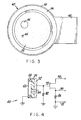
- a microphone 20 incorporating an electret constructed in accordance with our invention includes a conductive base or lower housing portion 22 and a conductive cap or upper housing portion 24 which fits over the base 22 in intimate sliding contact therewith as shown in FIGURE 1 to form a conductive housing.
- Cap 24 is formed with a port 26 and with a larger-diameter recess 28 on the outer side of the port for receiving a wire screen 30.
- base 22 is formed with a port 32 and with a larger-diameter recess 34 on the outer side of the port for receiving a wire screen 36.
- a circuit board 40 includes a circular portion, supported by the upper rim of base 22 inside the housing, and a rectangular exposed portion or tab 42, which extends out of the housing through a slot 44 formed in the sidewall of cap 24.
- a nonconductive outer epoxy seal 46 extends along the lower edge of cap 24 and along the interface between tab 42 and base 22.
- base 22 is formed with an indentation 48 around its lower periphery to accommodate the epoxy seal 46.
- Circuit board 40 which supports the transducer and electronic elements of the microphone 20, is formed from an insulating ceramic support 50 having a circular palladium-silver electrode 52 formed on the upper surface of the en closed portion of the board, as shown in FIGURE 3.
- a permanently polarized disk-shaped electret 54 (not shown in FIGURE 3) is formed on the upper surface of the electrode 52 in accordance with our invention, as described below.
- a concentric palladium-silver support ring 56 surrounding electrode 52 on the upper surface of the board 40 supports the periphery of the electret 54.
- Electret 54 in turn supports an annular spacer 58, preferably comprising a polyester material such as the one sold under the trademark MYLAR.
- Spacer 58 in turn has bonded thereto a diaphragm 60 also comprising a polyester such as MYLAR and having a gold plating (not separately shown) on its upper surface as viewed in FIGURE 1.
- Electrode 52, electret 54, spacer 58 and diaphragm 60 together constitute the transducer portion of the microphone 20.
- Board 40 is formed with a first, relatively large-diameter bore 64 to form an acoustic coupling between the two sides of the board.
- board 40 is formed with a smaller-diameter bore 66, which is plated through with palladium-silver to provide an electrical coupling between electrode 52 and a palladium-silver plated area 68 on the lower side of board 40 adjoining a gold plated area 70.
- Plated area 70 is connected to the gate electrode of a field-effect transistor (FET) 72 carried on the lower surface of board 40.
- FET field-effect transistor
- FET 72 has its source electrode coupled to a gold plated area 74 adjoining a palladium-silver plated area 76 and has its drain electrode coupled to a gold plated area 78 adjoining a palladium-silver plated area 80 also formed on the lower surface of board 40.
- a gate resistor 82 provides a conductive path between plated area 68 and a peripheral palladium-silver plated area 84 formed on the lower surface of board 40, while a source resistor 86 couples plated area 76 to the same peripheral area 84.
- a first electrical terminal or contact 88 formed on the lower surface of tab 42 extends inwardly through slot 44 to join plated area 84.
- a second electrical terminal 90 formed on the lower surface of tab 42 extends through slot 44 to join plated area 76, while a third terminal 92 formed on the lower surface of tab 42 extends inwardly through slot 44 to join plated area 80.
- terminals 88, 90 and 92 are formed of the same material as the plated areas that they join.
- a conductive epoxy layer 94 generally coextensive with annular plated area 84 couples area 84 electrically to base 22 and hence cap 24 to allow area 84 to serve as a ground or common line.
- Terminal 92 provides an external connection to the common plated area 84, while terminals 90 and 92 provide external connections to the source and drain, respectively, of FET 72, as shown in FIGURE 4.
- a nonconductive epoxy layer 96 separates the inwardly extending portions of terminals 90 and 92 from the upper rim of base 22 to preclude the possibility of a short circuit.
- a plurality of circuit boards 40 are formed from a single wafer 100, in which the circular portions of the boards and the sides of the tabs 42 are defined by laser cuts 102.
- the individual boards 40 are so arranged on the wafer 100 that the ends of the tabs 42 lie along lines 104 defined by scribes formed on the lower surface of the wafer 100.
- wafer 100 may be about 2.5 inches square and contain 33 individual boards 40.
- a ceramic wafer 100 is first drilled to form the bores 64 and 66 of the individual boards, and formed with laser cuts 102 and scribe lines 104 to permit the individual boards 40 to be snapped away from the remainder of the wafer along the scribe lines.
- the upper and lower surfaces of the individual boards 40 on the wafer 100 are then plated with areas of palladium-silver and gold, as described above.
- gate resistor 82 and source resistor 86 are screened onto the lower surfaces of the boards, as shown in FIGURE 2.
- mask 106 which rests on the surface of the wafer 100 during spraying, comprises a flat metal (e.g., brass) stencil formed with a plurality of apertures 108 concentric with and corresponding in diameter to the outside diameter of rings 56. Apertures 106 may be formed by any suitable process such as chemical etching.
- DuPont 856-200 TEFLON FEP clear coating an aqueous solution of FEP (fluorinated ethylene-propylene copolymer) having a viscosity of 25-300 centipoise (cP), is used.
- FEP fluorinated ethylene-propylene copolymer
- cP centipoise
- the material is preferably gently agitated at room temperature by rolling its container for 15 to 30 minutes, and then filtered through a 100 mesh stainless steel screen.
- Applicator 110 may comprise a standard compressed-air spray gun of the type used in painting.
- One suitable spray gun is a DeVilbiss Model MBC, operating at a pressure of 40 psi, with a #30 air cap with an F tip.
- the thickness of the applied dielectric layer 54 is controlled by the number of coatings. Preferably, no more than 1 mil of coating is formed per application.
- each coat of dielectric is applied in this manner to the front surface of wafer 100, it is thermally cured in accordance with the manufacturer's specifications to evaporate the solvent. Satisfactory results have been obtained with a total coating thickness of 1.5 mils, each coat being baked for 1 hour at 700°F.
- FETs 72 are applied to the lower surfaces of the individual boards 40, their leads bonded to gold-plated areas 70, 74 and 78, and the FETs potted over the epoxy (not shown).
- the individual boards are then separated from the wafer, as a preliminary to the charging step to be described below, by snapping them off at the ends of the tabs 42 along scribe lines 104.
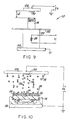
- the charging apparatus indicated generally by the reference numeral 112 includes a conductive support 114, the upper surface of which is formed with a well 116 for receiving an individual circuit board 40 with the lower surface thereof face down. As shown in FIGURE 10, well 116 is formed with a further recess 118 to accommodate the electronic components on the lower surface of the board 40.
- Support 114 rests on a brass workstation 120, which in turn has a conductive base 122.
- a resistive element 124 disposed within workstation 120 is adapted to be coupled to a source of potential v1 to heat the circuit board 40 to a suitable temperature during the charging process.
- a heat shield 126 disposed between support 114 and workstation 120 shields and electrode to be described from heat from the workstation 120.
- Conductive support 114 not only supports circuit board 40, but serves as a first electrode, to which the electrode 52 supporting the electret 54 is coupled through the electronic components on the lower surface of the board.
- a charging electrode 128 disposed at a predetermined distance d from support 114 is adapted to be coupled to a source of highly negative potential v2 to create a potential gradient in the region between electrode 128 and support 114.
- electrode 128 comprises a metal (e.g., brass) disk supported by suitable means (not shown) for pivotal movement between an operative position (FIGURES 9 and 10) in register with workstation 120 and support 114, with a breach or gap of width d, and an inoperative position out of register with support 114.
- ion generator 130 secured to the lower surface of electrode 128 ionizes the air in the region adjacent electrode 128, generating charged particles including positive ions 132, negative ions 134 and electrons 136.
- ion generator 130 comprises an alpha emitter such as polonium 210, which is a short-range, short-life material.
- the electrode 128 Since, as described above, the electrode 128 is maintained at a highly negative potential relative to support 114, positive ions 132 formed in the gap are attracted to electrode 128, while negative ions 135 and electrons 136 are attracted toward the support 114 and hence dielectric layer 54. Those electrons and negative ions that reach the dielectric 54 without recombining with positive ions impinge upon the surface of the dielectric layer 54. Owing to thermal activity in the dielectric layer 54, those electrons and negative ions are absorbed onto or into the material, producing a layer of a negative charge (not separately shown) at or adjacent to the upper surface of the dielectric layer. That charge remains when the charging electrode 128 is removed and the dielectric layer 54 cooled.
- an individual circuit board 40 on which a dielectric layer 54 has been formed is placed in the well 116 of support 114 and allowed to reach a suitable temperature.
- the electrode 128 and ion generator 130 are then swung into position opposite the support 114 at a spacing d therefrom.
- the dielectric layer 54 on board 40 is then charged for a predetermined time.
- the electrode 128 and ion generator 130 are then removed and the board 40 quickly cooled.
- To verify the charge level the board 40 is placed under an electrostatic voltmeter (not shown). If the measured voltage is acceptable, the board 40 is used to assemble a microphone as shown in FIGURES 1 to 4.
- the gap width d controls the rate and thus amount of charge on the surface of layer 54 for a given time, temperature and charging voltage v2.
- Suitable choices for the charging voltage v2, temperature, time and gap width d will be apparent to those skilled in the art. Satisfactory results have been obtained using a voltage v2 of -3000 volts, a time of 20 seconds, a temperature of 175°C and a gap width d of 0.5 inch.
Landscapes
- Engineering & Computer Science (AREA)
- Power Engineering (AREA)
- Physics & Mathematics (AREA)
- Microelectronics & Electronic Packaging (AREA)
- Acoustics & Sound (AREA)
- Signal Processing (AREA)
- Spectroscopy & Molecular Physics (AREA)
- Electrostatic, Electromagnetic, Magneto- Strictive, And Variable-Resistance Transducers (AREA)
Applications Claiming Priority (2)
| Application Number | Priority Date | Filing Date | Title |
|---|---|---|---|
| US35489389A | 1989-05-19 | 1989-05-19 | |
| US354893 | 1989-05-19 |
Publications (3)
| Publication Number | Publication Date |
|---|---|
| EP0397975A2 true EP0397975A2 (fr) | 1990-11-22 |
| EP0397975A3 EP0397975A3 (fr) | 1992-09-02 |
| EP0397975B1 EP0397975B1 (fr) | 1995-09-06 |
Family
ID=23395347
Family Applications (1)
| Application Number | Title | Priority Date | Filing Date |
|---|---|---|---|
| EP90104488A Expired - Lifetime EP0397975B1 (fr) | 1989-05-19 | 1990-03-09 | Procédé pour la fabrication d'un microphone à condenseur variable |
Country Status (5)
| Country | Link |
|---|---|
| EP (1) | EP0397975B1 (fr) |
| JP (1) | JPH0722440B2 (fr) |
| KR (1) | KR970004122B1 (fr) |
| CA (1) | CA2017185C (fr) |
| DE (1) | DE69022111T2 (fr) |
Cited By (2)
| Publication number | Priority date | Publication date | Assignee | Title |
|---|---|---|---|---|
| WO2000027166A3 (fr) * | 1998-11-02 | 2000-10-26 | Sarnoff Corp | Conception de transducteurs pour protheses auditives et autres dispositifs |
| WO2009112241A1 (fr) * | 2008-03-10 | 2009-09-17 | Sennheiser Electronic Gmbh & Co.Kg | Microphone à condensateur |
Families Citing this family (7)
| Publication number | Priority date | Publication date | Assignee | Title |
|---|---|---|---|---|
| JPH0992088A (ja) * | 1995-09-27 | 1997-04-04 | Daiichi Denso Buhin Kk | レバースイッチ |
| JPH0982178A (ja) * | 1995-09-07 | 1997-03-28 | Daiichi Denso Buhin Kk | レバースイッチ |
| AT409695B (de) * | 2001-05-18 | 2002-10-25 | Akg Acoustics Gmbh | Elektrostatisches mikrofon |
| KR20060058302A (ko) * | 2004-11-25 | 2006-05-30 | 주식회사 씨에스티 | 마이크로폰 조립체 |
| JP5459653B2 (ja) * | 2009-05-15 | 2014-04-02 | 日本放送協会 | 音響校正装置 |
| JP5283185B2 (ja) * | 2009-05-15 | 2013-09-04 | 日本放送協会 | エレクトレットの製造方法及びその製造装置 |
| JP5495363B2 (ja) * | 2009-05-15 | 2014-05-21 | 日本放送協会 | エレクトレットコンデンサの製造方法及びその製造装置 |
Family Cites Families (1)
| Publication number | Priority date | Publication date | Assignee | Title |
|---|---|---|---|---|
| GB1590472A (en) * | 1976-08-31 | 1981-06-03 | Nat Res Dev | Polymeric materials |
-
1990
- 1990-03-09 EP EP90104488A patent/EP0397975B1/fr not_active Expired - Lifetime
- 1990-03-09 DE DE69022111T patent/DE69022111T2/de not_active Expired - Fee Related
- 1990-05-18 CA CA002017185A patent/CA2017185C/fr not_active Expired - Fee Related
- 1990-05-18 JP JP2127033A patent/JPH0722440B2/ja not_active Expired - Fee Related
- 1990-05-19 KR KR1019900007288A patent/KR970004122B1/ko not_active Expired - Fee Related
Cited By (3)
| Publication number | Priority date | Publication date | Assignee | Title |
|---|---|---|---|---|
| WO2000027166A3 (fr) * | 1998-11-02 | 2000-10-26 | Sarnoff Corp | Conception de transducteurs pour protheses auditives et autres dispositifs |
| WO2009112241A1 (fr) * | 2008-03-10 | 2009-09-17 | Sennheiser Electronic Gmbh & Co.Kg | Microphone à condensateur |
| US8818004B2 (en) | 2008-03-10 | 2014-08-26 | Sennheiser Electronic Gmbh & Co. Kg | Condenser microphone |
Also Published As
| Publication number | Publication date |
|---|---|
| KR970004122B1 (ko) | 1997-03-25 |
| EP0397975B1 (fr) | 1995-09-06 |
| KR900019076A (ko) | 1990-12-24 |
| DE69022111T2 (de) | 1996-03-14 |
| CA2017185A1 (fr) | 1990-11-18 |
| JPH0722440B2 (ja) | 1995-03-08 |
| EP0397975A3 (fr) | 1992-09-02 |
| DE69022111D1 (de) | 1995-10-12 |
| JPH036500A (ja) | 1991-01-11 |
| CA2017185C (fr) | 1993-09-21 |
Similar Documents
| Publication | Publication Date | Title |
|---|---|---|
| US5101543A (en) | Method of making a variable capacitor microphone | |
| US4184188A (en) | Substrate clamping technique in IC fabrication processes | |
| JP6214054B2 (ja) | エレクトレット構体及びその製造方法並びに静電誘導型変換素子 | |
| EP0397975A2 (fr) | Procédé pour la fabrication d'un microphone à condenseur variable | |
| EP1843626A2 (fr) | Microphone à condensateur à électret semi-conducteur | |
| US4730283A (en) | Acoustic transducer with improved electrode spacing | |
| CN1706216B (zh) | 平行六面体型电容式传声器 | |
| US20070025570A1 (en) | Condenser microphone | |
| US20080130920A1 (en) | Capacitor microphone manufacturing method and capacitor microphone | |
| TWI830156B (zh) | 電漿處理裝置 | |
| US3702493A (en) | Method of making an electret | |
| JPH06303071A (ja) | 圧電装置の周波数同調方法とこの方法を実施する装置 | |
| US4232239A (en) | Frequency adjustment of piezoelectric resonator utilizing low energy oxygen glow device for anodizing electrodes | |
| US4375041A (en) | Terminal substrate for a quartz vibrating device | |
| KR20190142215A (ko) | 정전 척 및 그 제조 방법 | |
| JPH04221867A (ja) | セラミック圧電変換器ディスク及びその製造法 | |
| JPH06124792A (ja) | 除帯電電極 | |
| US4458161A (en) | Electret device | |
| WO2009147848A1 (fr) | Neutraliseur, procédé de polarisation d'électret de microphone par utilisation du neutraliseur, et dispositif de polarisation d'électret | |
| JP3591353B2 (ja) | カラー陰極線管およびその製造方法 | |
| JP2002218594A (ja) | シリコン酸化膜エレクトレットの製造方法、同製造方法によって得られたシリコン酸化膜エレクトレット、および、同シリコン酸化膜エレクトレットを備えたエレクトレットコンデンサマイクロホン | |
| JP2005142227A (ja) | プラズマ処理方法および処理装置 | |
| JPH04167425A (ja) | 同軸型プラズマ処理装置 | |
| JP2015159401A (ja) | エレクトレット材の製造方法およびエレクトレットコンデンサマイクロホン | |
| JPH01124218A (ja) | マスク基板のドライエッチング方法 |
Legal Events
| Date | Code | Title | Description |
|---|---|---|---|
| PUAI | Public reference made under article 153(3) epc to a published international application that has entered the european phase |
Free format text: ORIGINAL CODE: 0009012 |
|
| AK | Designated contracting states |
Kind code of ref document: A2 Designated state(s): BE CH DE FR GB LI LU NL |
|
| PUAL | Search report despatched |
Free format text: ORIGINAL CODE: 0009013 |
|
| AK | Designated contracting states |
Kind code of ref document: A3 Designated state(s): BE CH DE FR GB LI LU NL |
|
| 17P | Request for examination filed |
Effective date: 19930227 |
|
| 17Q | First examination report despatched |
Effective date: 19930525 |
|
| GRAA | (expected) grant |
Free format text: ORIGINAL CODE: 0009210 |
|
| AK | Designated contracting states |
Kind code of ref document: B1 Designated state(s): BE CH DE FR GB LI LU NL |
|
| REF | Corresponds to: |
Ref document number: 69022111 Country of ref document: DE Date of ref document: 19951012 |
|
| ET | Fr: translation filed | ||
| PLBE | No opposition filed within time limit |
Free format text: ORIGINAL CODE: 0009261 |
|
| STAA | Information on the status of an ep patent application or granted ep patent |
Free format text: STATUS: NO OPPOSITION FILED WITHIN TIME LIMIT |
|
| 26N | No opposition filed | ||
| REG | Reference to a national code |
Ref country code: GB Ref legal event code: IF02 |
|
| PGFP | Annual fee paid to national office [announced via postgrant information from national office to epo] |
Ref country code: LU Payment date: 20030228 Year of fee payment: 14 |
|
| PGFP | Annual fee paid to national office [announced via postgrant information from national office to epo] |
Ref country code: BE Payment date: 20030312 Year of fee payment: 14 |
|
| PGFP | Annual fee paid to national office [announced via postgrant information from national office to epo] |
Ref country code: CH Payment date: 20030320 Year of fee payment: 14 |
|
| PGFP | Annual fee paid to national office [announced via postgrant information from national office to epo] |
Ref country code: NL Payment date: 20030328 Year of fee payment: 14 |
|
| PG25 | Lapsed in a contracting state [announced via postgrant information from national office to epo] |
Ref country code: LU Free format text: LAPSE BECAUSE OF NON-PAYMENT OF DUE FEES Effective date: 20040309 |
|
| PG25 | Lapsed in a contracting state [announced via postgrant information from national office to epo] |
Ref country code: BE Free format text: LAPSE BECAUSE OF NON-PAYMENT OF DUE FEES Effective date: 20040331 Ref country code: CH Free format text: LAPSE BECAUSE OF NON-PAYMENT OF DUE FEES Effective date: 20040331 Ref country code: LI Free format text: LAPSE BECAUSE OF NON-PAYMENT OF DUE FEES Effective date: 20040331 |
|
| BERE | Be: lapsed |
Owner name: *GENTEX CORP. Effective date: 20040331 |
|
| PG25 | Lapsed in a contracting state [announced via postgrant information from national office to epo] |
Ref country code: NL Free format text: LAPSE BECAUSE OF NON-PAYMENT OF DUE FEES Effective date: 20041001 |
|
| REG | Reference to a national code |
Ref country code: CH Ref legal event code: PL |
|
| NLV4 | Nl: lapsed or anulled due to non-payment of the annual fee |
Effective date: 20041001 |
|
| PGFP | Annual fee paid to national office [announced via postgrant information from national office to epo] |
Ref country code: GB Payment date: 20080305 Year of fee payment: 19 |
|
| PGFP | Annual fee paid to national office [announced via postgrant information from national office to epo] |
Ref country code: FR Payment date: 20080311 Year of fee payment: 19 Ref country code: DE Payment date: 20080306 Year of fee payment: 19 |
|
| GBPC | Gb: european patent ceased through non-payment of renewal fee |
Effective date: 20090309 |
|
| REG | Reference to a national code |
Ref country code: FR Ref legal event code: ST Effective date: 20091130 |
|
| PG25 | Lapsed in a contracting state [announced via postgrant information from national office to epo] |
Ref country code: DE Free format text: LAPSE BECAUSE OF NON-PAYMENT OF DUE FEES Effective date: 20091001 |
|
| PG25 | Lapsed in a contracting state [announced via postgrant information from national office to epo] |
Ref country code: GB Free format text: LAPSE BECAUSE OF NON-PAYMENT OF DUE FEES Effective date: 20090309 Ref country code: FR Free format text: LAPSE BECAUSE OF NON-PAYMENT OF DUE FEES Effective date: 20091123 |