EP0398593A2 - Vorrichtung zur Anzeige übermässiger Quetschung einer Kabelanordnung gegen eine elektrisch geerdete Struktur - Google Patents
Vorrichtung zur Anzeige übermässiger Quetschung einer Kabelanordnung gegen eine elektrisch geerdete Struktur Download PDFInfo
- Publication number
- EP0398593A2 EP0398593A2 EP90305075A EP90305075A EP0398593A2 EP 0398593 A2 EP0398593 A2 EP 0398593A2 EP 90305075 A EP90305075 A EP 90305075A EP 90305075 A EP90305075 A EP 90305075A EP 0398593 A2 EP0398593 A2 EP 0398593A2
- Authority
- EP
- European Patent Office
- Prior art keywords
- layer
- semiconductive
- cable
- detector circuit
- cable arrangement
- Prior art date
- Legal status (The legal status is an assumption and is not a legal conclusion. Google has not performed a legal analysis and makes no representation as to the accuracy of the status listed.)
- Granted
Links
Images




Classifications
-
- G—PHYSICS
- G01—MEASURING; TESTING
- G01R—MEASURING ELECTRIC VARIABLES; MEASURING MAGNETIC VARIABLES
- G01R31/00—Arrangements for testing electric properties; Arrangements for locating electric faults; Arrangements for electrical testing characterised by what is being tested not provided for elsewhere
- G01R31/50—Testing of electric apparatus, lines, cables or components for short-circuits, continuity, leakage current or incorrect line connections
- G01R31/58—Testing of lines, cables or conductors
Definitions
- This invention relates generally to the field of cable failure detection, and more particularly, to an apparatus for detecting excessive chafing of a cable arrangement against an electrically grounded structure prior to actual cable failure.
- chafing between a pair of objects occurs when the pair of objects are brought into contact with each other and relative motion between the objects takes place. It is further well recognized that continued chafing between the pair of objects will, over time, result in erosion-induced damage to one or both of the objects.
- the chafing which occurs when an electrical cable which forms a portion of an electrical system contacts the system hardware or support structure at some point along the cable's length and relative motion, i.e., chafing, between the cable and structure occurs. This relative motion can result from vibration of or within the electrical system, or from the frequent removal and installation of a replaceable unit to which the cable is attached.
- the exact location of the failure may be detected utilizing presently available test or detection equipment only if contact is maintained between the current-carrying conductor of the chafed cable and the grounded structural member or equipment support hardware. If the current-carrying conductor of the chafed cable is only momentarily brought into contact with the grounded structural member or system support hardware (as in the case of transient chafing due to vibration), conventional failure detection equipment is incapable of determining the exact location of the cable failure.
- the chief object of the present invention is to provide an apparatus which includes a covering positioned in surrounding relation with an electrical cable or other tubing which is operable in conjunction with a detector circuit connected therewith to detect chafing of the covering against an electrically grounded structural member.
- the invention provides an apparatus for detecting excessive chafing of a cable arrangement against an electrically grounded structure, comprising: an elongated member of preselected length having a pair of opposing end portions and an outer surface extending therebetween; a layer of semiconductive material positioned in surrounding relation with said outer surface of said elongated member and extending over a predetermined length of said member; a layer of electrically insulating material surrounding said layer of semiconductive material; said elongated member, layer of semiconductive material and layer of electrically insulating material forming said cable arrangement; detector circuit means electrically connected with said layer of semiconductive material; and said detector circuit means including means for detecting at least momentary contact between said layer of semiconductive material and said electrically grounded structure due to erosion of said layer of electrically insulating material caused by excessive chafing of said layer of electrically insulating material against said grounded structure; whereby said contact between said layer of semiconductive material forming a portion of said cable arrangement and said electrically grounded structure is detected by
- the invention further provides a plurality of cable arrangements each connected with apparatus for detecting excessive chafing of at least one of said arrangements against an electrically grounded structure, comprising: a plurality of elongated members each having a preselected length, a pair of opposing end portions and an outer surface extending therebetween; a layer of semiconductive material positioned in surrounding relation with the outer surface of each said elongated member and extending over a preselected length of said member; a layer of electrically insulating material surrounding each layer of semiconductive material; said plurality of elongated members each having a layer of semiconductive material and a layer of electrically insulating material positioned in surrounding relation therewith forming a plurality of cable arrangements; multiplexing means having a plurality of inputs and an output, the layer of semiconductive material of one of said plurality of cable arrangements being electrically connected with one of said inputs; a plurality of detector circuit means each electrically connected with said output of said multiplexing means; said multiplexing means being operable to electrically
- apparatus for detecting excessive chafing between a cable arrangement and an electrically grounded structure which includes an elongated member of preselected length having a pair of opposing end portions and an outer surface extending therebetween.
- a layer of semiconductive material is positioned in surrounding relation with the outer surface of the elongated member and extends over a predetermined length thereof.
- a layer of electrically insulating material surrounds the layer of semiconductive material. The elongated member, layer of semiconductive material and layer of electrically insulating material form the cable arrangement.
- a detector circuit is electrically connected with the layer of semiconductive material, and includes means for detecting at least momentary contact between the layer of semiconductive material and an electrically grounded structure due to erosion of the layer of electrically insulating material caused by excessive chafing of the layer of electrically insulating material against the grounded structure.
- the detector circuit is operable to detect the contact of the layer of semiconductive material forming a portion of the cable arrangement with the electrically grounded structure prior to actual chafing of the elongated member against the electrically grounded structure.
- apparatus for detecting excessive chafing between a cable arrangement and an electrically grounded structure which includes an elongated member of preselected length having a pair of opposing end portions and an outer surface extending therebetween.
- a layer of semiconductive material is positioned in surrounding relation with the outer surface of the elongated member and extends over a predetermined length thereof.
- the layer of semiconductive material includes a first reference end portion and an opposite second end portion.
- a layer of electrically insulating material surrounds the layer of semiconductive material.
- the elongated member, layer of semiconductive material and layer of electrically insulating material form the cable arrangement.
- a detector circuit is electrically connected with the layer of semiconductive material at the semiconductive material reference end portion.
- the detector circuit includes means for detecting contact between the layer of semiconductive material and an electrically grounded structure due to erosion of the layer of electrically insulating material caused by excessive chafing of the layer of electrically insulating material against the grounded structure.
- the detector circuit further includes means for providing an indication of the distance measured along the layer of semiconductive material between the semiconductive layers' reference end portion and the location at which the layer of semiconductive material contacts the grounded structure.
- the detector circuit further includes means for providing an indication that the layer of semiconductive material has at least momentarily contacted the electrically grounded structure in the event the layer of semiconductive material initially contacts the grounded electrical structure and is thereafter removed from contact there from.
- apparatus for detecting excessive chafing between at least one of a plurality of cable arrangements and an electrically grounded structure which includes a plurality of elongated members each having a preselected length, a pair of opposing end portions, and an outer surface extending therebetween.
- a layer of semiconductive material is positioned in surrounding relation with the outer surface of each elongated member and extends over a preselected length of each member.
- a layer of electrically insulating material surrounds each layer of semiconductive material.
- the plurality of elongated members each having a layer of semiconductive material and a layer of electrically insulating material positioned in surrounding relation therewith form a plurality of cable arrangements.
- Multiplexing means having a plurality of inputs and an output.
- the layer of semiconductive material of one of the plurality of cable arrangements is electrically connected with one multiplexing means input.
- a plurality of detector circuits are connected with the output of the multiplexing means.
- the multiplexing means is operable to electrically connect, in succession, the semiconductive layer of a preselected one of the plurality of cable arrangements with a preselected one of the plurality of detector circuits.
- the preselected detector circuit is operable when electrically connected with the preselected cable arrangement semiconductive layer to detect contact between the preselected cable arrangement semiconductive layer and an electrically grounded structure due to the erosion of the electrically insulating layer surrounding the preselected cable arrangement semiconductive layer caused by excessive chafing of the preselected cable arrangement electrically insulating layer against the grounded structure.
- apparatus for use with an elongated member of preselected length for preventing the member itself from chafing against an electrically grounded structure which includes a layer of semiconductive material arranged to be positioned in surrounding relation with the outer surface of the elongated member and extend over a predetermined length of the member.
- a layer of electrically insulating material surrounds the layer of semiconductive material.
- a detector circuit is electrically connected with the layer of semiconductive material. The detector circuit includes means for detecting at least momentary contact between the layer of semiconductive material and an electrically grounded structure due to erosion of the layer of electrically insulating material caused by excessive chafing of the layer of electrically insulating material against the grounded structure. The contact between the layer of semiconductive material and the electrically grounded structure is detected by the detector circuit prior to actual chafing of the elongated member itself against the electrically grounded structure.
- the sacrificial covering surrounds the cable or other tubing, and any chafing-induced erosion experienced by the cable/sacrificial covering arrangement will take place in the covering rather than in the cable.
- the detector circuit to be described is operable to provide an indication of chafing-induced erosion of the sacrificial covering well before the cable itself experiences actual chafing against the grounded structural member. This timely indication will allow the chafing condition to be corrected prior to chafing-induced failure of the cable or tubing itself.
- the detector circuit to be described is capable of providing an indication of the distance to the chafing location measured from a reference end of the sacrificial covering in order to avoid the need for a visual inspection of the entire covering to locate the chafe.
- the detector circuit to be described is capable of providing an indication of chafing-induced erosion of the sacrificial covering in the event that the chafing is transient or intermittent.
- an electrical cable 10 which includes an outer insulating jacket 12 surrounding a plurality of individual conductors 14.
- Each conductor 14 includes an outer insulating jacket 15 and a current-carrying conductor 17.
- Electrical cable 10 has a preselected length, and includes a pair of opposing end portions 16, 18 with the outer insulating surface 20 of the insulating jacket extending therebetween. Cables such as electrical cable 10 are themselves well known in the art, and may be used to connect a plurality of individual electrical components which are physically spaced from each other yet form part of a single electrical system.
- cable 10 Due to the spacing between the individual components which may be electrically connected via cable 10, cable 10 normally will be positioned in contacting relation at one or more points along its length with structural support members. In addition, depending upon the environment in which electrical cable 10 is located, cable 10 may be positioned in contacting relation with operating structures controlled by the electrical system. It is apparent that if cable 10 is positioned in contacting relation at various points along its length with structural support members or other operating structures, any relative motion between electrical cable 10 and these structures will result in chafing of the electrical cable outer insulating jacket 12 at one or more of these contact areas.
- cable 10 may itself be enclosed in a sacrificial covering 22 which forms a portion of the chafing detector apparatus 24 of the present invention.
- chafing detector apparatus 24 includes sacrificial covering 22 in surrounding relation with the outer surface 20 of electrical cable 10 insulating jacket 12.
- sacrificial covering 22 includes a layer of semiconductive material 26 positioned in surrounding, contacting relation with outer surface 20 and having an overall length L t to extend over a predetermined length of the cable.
- a layer of electrically insulating material 28 is positioned in surrounding, contacting relation with semiconductive layer 26.
- Electrically insulating layer 28 also has an overall length L t to completely surround semiconductive layer 26 over its entire length.
- Figs. 1 and 2 may be formed, for example, from a semiconductive rubber tape, and the layer of electrically insulating material 28 illustrated in Figs. 1 and 2 may be formed from either a PVC electrical tape or a polymer spiral wrap.
- Other suitable semiconductive materials which may be utilized to form layer 26 include carbon particle-filled coatings, carbon plus metallic particle-filled coatings, intrinsic semicon ductive polymer coatings, for example polypyrole, and conductive particle-filled intrinsic semiconductive polymer coatings.
- electrically insulating layer 28 may be formed from an insulating polymer coating. Both layers 26 and 28 may, if desired, be applied by a variety of techniques such as dipping, spraying or brushing, for example.
- both the semiconductive and electrically insulating layers 26, 28 may be formed, if desired, from still other suitable materials.
- the electrical cable 10 and sacrificial covering 22 arrangement illustrated in Figs. 1 and 2 form a cable arrangement generally designated by the numeral 29.
- forming layer 26 from a semiconductive material i. e., a material which has, for example, a resistance of 100 ohms to 1000 ohms per foot, permits the use of methods to detect chafing of cable arrangement 29 against a grounded structural member that are impractical using existing fault location equipment such as precision wheatstone bridge equipment.
- semiconductive layer 26 and electrically insulating layer 28 forming sacrificial covering 22 extend over a length L t of cable 10 intermediate the cables' end portions 16, 18.
- Semiconductive layer 26 includes a first, reference end portion 30 and an opposite second end portion 32.
- a detector circuit generally designated by the numeral 34 which also forms a portion of the chafing detector apparatus 24 of the present invention, is connected with semiconductive layer 26 at reference end portion 30.
- detector circuit 34 is operable to detect chafing between cable arrangement 29 and a grounded structural member such as member 36 schematically illustrated in Fig.
- the detector circuit 34 of the present invention is also operable to provide an indication of the distance measured along semiconductive layer 26 between the reference end portion 30 and the location or area at which semiconductive layer 26 actually contacts the grounded structural member 36. For example, as seen in Fig.
- detector circuit 34 will provide the value L f or a value proportional thereto so that the exact location of the chafe may be determined and the chafing condition eliminated through repair of the sacrificial layer 22 insulating layer 28.
- This feature is extremely desirable in that since the overall length of electrical cable 10 and sacrificial covering 22 may be quite long, an excessive amount of time would otherwise be required to inspect the entire length of sacrificial covering 22 to determine the exact location of the chafe-induced contact.
- detector circuit 34 By providing a detector circuit such as detector circuit 34 which is capable of determining the exact location of the chafe, the chafed area may be quickly located and repaired.
- detector circuit 34 is also operable to provide an indication that semiconductive layer 26 has at least momentarily contacted electrically grounded structure 36 in the event that the chafing condition itself is transient, 1. e., vibration induced. It is apparent that if cable 10 is used in an environment which causes the cable to be subjected to extreme or prolonged vibration, or in an environment which causes the cable to be subjected to high G forces, chafing of cable arrangement 29 against grounded structural member 36 may only be intermittent.
- the cable arrangement/detector circuit of the present invention is an improvement over known test equipment capable of detecting a chafing condition only in the event that the individual current- carrying conductors 14 of cable 10 contact grounded structural member 36 through erosion of insulating jacket 12 and contact between the conductors and the grounded member is maintained, i.e., a hard fault.
- known test equipment is capable of detecting intermittent contact between the conductors 14 of cable 10 and grounded structural member 36 only in the fortuitous event that the test equipment is used at the precise instant of time that contact between the conductors and grounded member is made.
- the cable arrangement/detector circuit of the present invention is, on the other hand, capable of detecting chafing between the cable arrangement and a grounded structural member even if only a single, momentary contact between the cable arrangement semiconductive layer and the grounded member takes place.
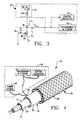
- FIG. 3 there is schematically illustrated detector circuit 34 connected with the reference end portion 30 of semiconductive layer 26 forming a portion of cable arrangement 29.
- semiconductive layer 26 has an overall length L t , and includes the first, reference end portion 30 and opposite end portion 32. Since layer 26 is made from a semiconductive material, layer 26 has a resistance per unit length which is greater than the resistance per unit length of a straight conductive material. As previously stated, this permits the use of methods to detect chafing between cable arrangement 29 and grounded member 36 that are impractical using existing fault location equipment.
- Detector circuit 34 includes a power source generally designated by the numeral 40, and a V measurement and storage device generally designated by the numeral 42 which provides a chafing indication at 44.
- chafing indication 44 may be any suitable logic driven device, such as an LED, buzzer or bell. It should be understood that although power source 40 is illustrated in Fig. 3 as including a regulated voltage source 46 and internal series resistance 48, power source 40 may also be illustrated as known in the art as a constant current source.
- the value of the voltage V present at reference end portion 30 is substantially the same as V s supplied by voltage source 46. Under this condition, the value, of the currents I1 and I2 are substantially zero. However, when semiconductive layer 26 contacts grounded structural member 36 at contact area 38 due to excessive erosion of the electrically insulating layer 28 (shown in Figs. 1 and 2) against the grounded structural member, the value of the voltage V at the reference end portion 30 of semiconductive layer 26 falls below V s .
- the distance between the reference end portion 30 of semiconductive layer 26 and the point of contact between semiconductive layer 26 and grounded structural member 36 which is represented as L f in Fig. 3, may be calculated as follows: where V s equals the voltage supplied by voltage source 46, R s equals the fixed series resistance 48 of voltage source 46, V equals the voltage at reference end portion 30 and R0 equals the resistance per unit length of semiconductive layer 26.
- the distance from the reference end portion 30 of semiconductive layer 26 to the chafing area 38 may be calculated assuming that I1 is much greater than I2. This assumption is valid since V measurement and storage device 42 has a high input impedance. As will be explained further herein, device 42 detects the chafing contact between grounded structural member 36 and semiconductive layer 26 at contact area 38, provides a voltage signal output proportional to the value of L f and provides an indication of contact via circuit 44 even if the contact is momentary or transient.
- detector circuit 34 will be described later herein with reference to Figs. 9 through 12.
- sacrificial covering 22 which forms a portion of the chafing detector apparatus 24 of the present invention.
- semiconductive and electrically insulating layers 26, 28 may respectively be formed, for example, from semiconducting rubber tape and either a PVC electrical tape or a polymer spiral wrap.
- the sacrificial coverings 22 embodied in Figs. 4-7B may also be utilized with similar results.
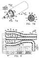
- chafing detector apparatus 24 includes the detector circuit 34 previously described and sacrificial covering 22 positioned in surrounding relation with electrical cable 10.
- Sacrificial covering 22 includes the layer of semiconducting rubber tape 26 positioned in surrounding, contacting relation with the outer surface 20 of electrical cable 10 insulating jacket 12.
- a layer of electrically insulating material 28 in the form of a polybutylene terephthalate (PBT) expandable braided sleeving is positioned in surrounding relation with semiconductive layer 26.
- PBT polybutylene terephthalate
- the benefit to using a PBT expandable braided polymer sleeving as the insulating layer of cable arrangement 29 is that the braided polymer sleeving is very easily and rapidly applied, maintains its integrity to temperatures in excess of 125°C and is extremely flexible.
- FIGs. 5A and 5B there is illustrated still another alternate embodiment of the sacrificial covering 22 forming a portion of the chafing detector apparatus 24 of the present invention.
- an electrically insulating, expandable braided polymer sleeve 54 is positioned in surrounding, contacting relation with the outer surface 20 of electrical cable 10 insulating jacket 12.
- Expandable braided polymer sleeve 54 has a generally annular cross-sectional configuration to define an inner surface 56 in contact with jacket 12 outer surface 20, an outer surface 58 substantially concentric with inner surface 56 and an annular wall 60 extending between inner and outer surfaces 56, 58.
- the inner surface 56 and a first predetermined portion 62 of the annular wall 60 adjacent to inner surface 56 are subjected to a preselected dosage of ion irradiation by means well known in the art to impart semiconductive properties to inner surface 56 and the predetermined portion 62 of annular wall 60.
- the remaining portion 64 of annular wall 60 and outer surface 58 are not subjected to ion irradiation, and thus remain an electrically insulating polymer.
- the process of ion irradiating or bombarding polymers with energetic ions to convert the polymer to a semiconductive material is itself known in the art.
- the ion beam energy and beam flux determine the ultimate conductivity of the semiconductive layer.
- This process can be used with most polymeric materials, and produces a thin semiconductive layer at the surface of the irradiated material.
- electrically insulating/expandable braided polymer sleeve 54 to an ion irradiation process, the inner surface 56 and a predetermined portion 62 of annular wall 60 may be converted to a semiconductive material.
- the remaining annular portion 64 of polymer sleeve 54 remains an electrically insulating polymer.
- both the semiconductive and electrically insulating layers 26, 28 previously described herein with reference to Figs. 1, 2 and 4 may be formed from a single expandable braided polymer sleeve. That is, semiconductive layer 26 corresponds to the predetermined portion 62 of annular wall 60 subject to ion irradiation and electrically insulating layer 28 corresponds to the remaining portion 64 of annular wall 60.
- the advantage of forming both the semiconductive and electrically insulating layers of sacrificial covering 22 from a single material are that both the semiconductive and electrically insulating layers may be applied to a cable such as electrical cable 10 in a single operation, and the expandable braided sleeving may be easily and rapidly repaired.
- sacrificial covering 22 includes a first expandable braided polymer sleeve 66 positioned in surrounding, contacting relation with the outer surface 20 of electrical cable 10 insulating jacket 12.
- First sleeve 66 has a generally annular cross-sectional configuration to define an inner surface 68 in contacting relation with the outer surface 20 of jacket 12, and outer surface 70 substantially concentric with inner surface 68 and an annular wall 72 extending between inner and outer surfaces 68, 70.
- the inner surface 68 and a first predetermined portion 74 of annular wall 72 adjacent to inner surface 68 of first polymer sleeve 66 have the properties of an electrical insulating material.
- the remaining, second portion 76 of annular wall 72 and the outer surface 70 of first polymer sleeve 66 are subjected to a preselected dosage of ion irradiation and thereby converted to a semiconductive material.
- first expandable braided polymer sleeve 66 has an annular wall extending between its inner and outer surfaces, a portion of the annular wall adjacent to the inner surface and the inner surface itself forming an electrically insulating layer and the remaining portion of the annular wall and the annular wall outer surface forming a layer of semiconductive material.
- a second expandable braided polymer sleeve 78 is positioned in surrounding, contacting relation with the outer surface 70 of first polymer sleeve 66 and forms an electrically insulating layer.
- first polymer sleeve 66 forms a semiconductive layer
- second expandable braided polymer sleeve 78 forms an electrically insulating layer.
- These respective layers correspond to the semiconductive and electrically insulating layers 26, 28 described with respect to Figs. 1, 2 and 4.
- sacrificial covering 22 is formed from a single section of polymer tubing 80 having an inner surface 82 in surrounding, contacting relation with the outer surface 20 of electrical cable 10 insulating jacket 12.
- Polymer tubing 80 further includes an outer surface 84 substantially concentric with inner surface 82, and an annular wall 86 extending between inner and outer surfaces 82, 84.
- a first predetermined portion 88 of annular wall 86 adjacent to inner surface 82 and inner surface 82 are subjected to a preselected dosage of ion irradiation by means well known in the art to form a layer of semiconductive material.
- the first preselected portion 88 of annular wall 86 corresponds to the layer of semiconductive material 26 previously described with respect to Figs. 1, 2 and 4 and the second preselected portion 90 of annular wall 88 corresponds to electrically insulating layer 28.
- each sacrificial covering 22 includes a layer of semiconductive material 26 positioned in surrounding, contacting relation with the outer surface of one of the cables 94, 96, 98 (outer surfaces designated as 100, 102, 104, respectively).
- a layer of electrically insulating material 28 surrounds each semiconductive layer 26.
- each of the electrical cables, 94, 96, 98 has a sacrificial covering positioned therearound, each sacrificial covering being formed from a layer of semiconductive material and a layer of electrically insulating material. It should be understood that although three electrical cables 94, 96, 98 are illustrated in Fig. 8, any desired number of electrical cables may be utilized with the chafing detector apparatus of the present invention.
- the layer of semiconductive material 26 of each sacrificial covering 22 includes a reference end portion 30, and each reference end portion 30 is connected with a multiplexing detector circuit generally designated by the numeral 106 which also forms a portion of the chafing detector apparatus of the present invention.
- multiplexing detector circuit 106 and the sacrificial coverings 22 surrounding each of the electrical cables 94, 96, 98 are operable, in combination, to detect when the electrically insulating layer 28 of at least one of the sacrificial coverings 22 surrounding the cables 94, 96, 98 erodes sufficiently due to chafing against a grounded structure to permit contact between the semiconductive layer beneath the eroded electrically insulating layer and the grounded structure.
- a desired number of elongated members may each be enclosed in a sacrificial covering formed from layers of semiconductive and electrically insulating material.
- Each of the elongated members enclosed in a single sacrificial covering is referred to as a cable arrangement.
- Each cable arrangement is connected with a detector circuit, the detector circuit being operable to provide an indication of excessive chafing of the cable arrangement against an electrically grounded structural member and to provide an indication of the distance measured along the length of the cable arrangement from a reference end portion of the cable arrangement to the chafing area.
- the detector circuit utilized herein is further operable to provide an indication of a chafing condition even in the event that the chafing condition is transient in nature.
- FIGs. 9-14 there are illustrated various embodiments of the detector circuit 34 and multiplexing detector circuit 106 previously described with reference to Figs. 1-8.
- the various detector circuits schematically illustrated in Figs. 9-12 correspond to the detector circuits illustrated in Figs. 1-7A, and are further utilized as building blocks for the multiplexing detector circuits illustrated in Figs. 13 and 14.
- Analog Detector circuit 34 includes a power source 40 in the form of a constant current source, and a V measurement and storage circuit generally designated by the numeral 42. Both power source 40 and V measurement and storage circuit 42 are connected with the reference end portion 30 of the schematically illustrated semiconductive layer 26 previously described. In the event that the semiconductive layer 26 is insulated from grounded structural member 36, then no current flows through the semiconductive layer. In this situation, the voltage V at the input to V measurement and storage circuit 42 will approximate the power source voltage V S .
- Low pass filter 122 is utilized to minimize the effect of noise resulting from erratic contact with structural member 36. If required, low pass filter 122 may also be utilized to scale the value of V.
- the output of low pass filter 122, designated V LP is supplied to a track and hold circuit 124 on line 126. As known in the art, because of the capacitor charging time within track and hold circuit 124, the output voltage V out on line 128 will lag the input voltage V LP by a small amount.
- a chafe (semiconductive layer 26 contacting grounded structural member 36 at some point along its length) is defined as: the input voltage V is below a predefined value set by the constant current source multiplied by the maximum cable resistance, and the voltage V at the moment of contact between semiconductive layer 26 and grounded structural member 36 has reached its lowest value and is beginning to rise.
- a comparator 130 is utilized to detect the excursion of the voltage V at the moment of contact below the predefined voltage limit.
- a second comparator 132 is utilized to determine when the voltage V out , which lags behind the input voltage V LP , is less than the input voltage V LP . At this point, the circuit assumes that the input has hit a negative peak and has started to rise. These two conditions cause the flip flow 134 to latch, and cause the track and hold circuit 124 to stop tracking and hold the voltage V at its negative peak.
- the failure condition latched in flip flop 134 will be used to alert personnel of a chafing condition via chafing indication 44.
- Indication 44 may be any suitable logic driven device, such as an LED, buzzer or bell.
- Reset circuit 136 including resistor R3, capacitor C1, diode D1 and switch S1 form the reset network that will cause the fault memory to be cleared upon startup.
- Track and hold circuit 124 provides a V out on line 128 that is directly proportional to the distance measured along semiconductive layer 26 from reference end portion 30 to the point at which semiconductive layer 26 contacts electrically grounded structure (L f ). By utilizing known scaling techniques, track and hold circuit 124 may be adjusted to provide that the numerical value of V out corresponds to the length L f . In this manner, the exact distance from the reference end portion of the cable arrangement to the chafing point may be determined and displayed with accuracy.
- the pair of comparators 130, 132 provide an input at the S-terminal of R-S flip flop 134 via NAND gate 140, and flip flop 134 provides an indication when semiconductive layer 26 has contacted grounded structural member 36.
- V measurement and storage circuit 42 also includes means for maintaining an indication of contact between semiconductive layer 26 and grounded structural member 36 even after the contact is broken due to vibration or some other transient condition. The indication of contact will be maintained on line 144 until R-S flip flop 134 is reset.
- V measurement and storage circuit 42 forming a portion of detector circuit 34 may, by utilizing analog techniques, provide an indication that excessive chafing of the cable arrangement has taken place, and further provide an indication of the distance measured from a reference end portion of the cable arrangement to the location of the chafe.
- detector circuit 34 includes a power source 40 in the form of a constant current source and a V measurement and storage circuit generally designated by the numeral 42. Both the power source 40 and V measurement and storage circuit 42 are connected with the reference end portion 30 of schematically illustrated semiconductive layer 26.
- the analog detector circuit 34 illustrated in Fig. 9, so long as semiconductive layer 26 is isolated from grounded structural member 36, no current flows in the semiconductive layer 26 and the voltage V at reference end portion 30 will approximate the supply voltage V S .
- Momentary contact between semiconductive layer 26 and grounded structural member 36 will place negative-going transients at the input 144 to low pass filter 146.
- Low pass filter 146 is utilized to minimize the effect of noise as previously described with respect to the analog circuit of Fig. 9. If desired, the low pass filter 146 may also be used to scale the value of V.
- the output of low pass filter 146, designated as V LP is supplied on line 148 to an A-D converter 150.
- the V measurement and storage circuit 42 of Fig. 10 recognizes that a chafe condition has occurred when the input voltage V to low pass filter 146 falls below a predefined value set by constant source current 40 multiplied by the maximum resistance of semiconductive layer 26, and the voltage V has reached its lowest value upon contact between semiconductive layer 26 and grounded structural member 36 and has started to rise.
- V measurement and storage circuit 42 includes a comparator 154 utilized to detect the excursion of V below the predefined limit.
- Comparator 152 is utilized to determine when the output voltage V out of converter 150 on line 156 is greater than the previous sample held in register 158. At this point, circuit 42 assumes that V has hit a negative peak and has started to rise. These two conditions cause latch and hold circuit 160 to provide a fault indicating logic signal to chafing indication device 44 on line 162.
- the current value of the V negative peak is held in register 158 and output on line 159. This value is a digital representation of the distance from the reference end portion 30 of semiconductive layer 26 to the contact area between semiconductive layer 26 and electrically grounded structure 36.
- the comparator 154 includes an input 166 for receiving the predefined or threshold value against which V is compared to determine whether or not an actual contact between semiconductive layer 26 and grounded structural member 36 has occurred; and is also used to detect a voltage rise once comparator 152 has fallen below the predefined limit. It should be understood that although V measurement and storage circuit 42 illustrated in Fig. 10 is formed from discrete components, all of the functions performed by circuit 42 may be implemented utilizing a microprocessor.
- detector circuit 34′ includes the power source 40 and V measurement and storage circuit 42 previously described with respect to Fig. 9.
- detector circuit 34′ includes a built-in-test (BIT) circuit generally designated by the numeral 168.
- BIT circuit 168 permits an additional level of testing for both the schematically illustrated semiconductive layer 26 and the detector circuit itself. If BIT circuit 168 is utilized, a resistor 170 is connected with the opposite end portion 32 of semiconductive layer 26 at point 172. Resistor 170 itself is grounded.
- BIT built-in-test
- BIT detector 168 further includes a transistor 183 and resistor 184 which form an optional fault circuit which may be used to test trip the detector circuit.
- the value of resistor 184 is selected so that the parallel combination of semiconductive layer 26, resistor 170 and resistor 184 will provide a known chafe condition at, for example, 50% of the overall length of the semiconductive layer.
- the base 186 of transistor 183 is connected to voltage source V S through a pushbutton 188 and resistor 190. Closing pushbutton 188 initiates a test trip of detector circuit 34′ by providing current to the base 186 of transistor 183 of sufficient magnitude to switch transistor 183 on and allow current to flow through the emitter-collector junction of the transistor to ground.
- Detector circuit 34′ illustrated in Fig. 12 includes built-in-test (BIT) circuit 191 to allow an additional level of testing of both semiconductive layer 26 and detector circuit 34. If BIT circuit 191 is utilized, then resistor 192 is connected with the end portion 32 of semiconductive layer 26 at connection point 194. Connecting semiconductive layer 26 to ground via resistor 192 will allow current generated by power source 40 to flow through the semiconductive layer and resistor 192, producing a voltage drop across semiconductive layer 26.
- BIT built-in-test
- the voltage V at the input to low pass filter 146 will rise above a threshold voltage value supplied to comparator 196 of bit detector 191 on input line 198. This sets the BIT failure latch 200, and a BIT failure signal is provided from BIT failure latch 200 on output line 202.
- semiconductive layer 26 will be shorted to ground via grounded structural member 36 to lower the total resistance of the semiconductive layer to a preselected fraction of the overall semiconductive layer resistance. This causes the voltage V to drop below the same predefined value described with respect to Figure 10, and a failure will be detected.
- resistor 192 is assumed to be negligible with respect to the effect of grounding of semiconductive layer 26.
- Transistor 204 and resistor 206 may be connected in parallel with semiconductive layer 26 and resistor 192 to provide a test mode for BIT detector 191.
- the value of resistor 206 is selected so the parallel combination of the resistance of semiconductive layer 26, resistor 192 and resistor 206 will simulate a known "chafe" condition at, for example, 50% of the overall length of semiconductive layer 26.
- a pushbutton 208 and resistor 210 are connected with the base 212 of transistor 204 to provide current to the transistor base and switch transistor 204 "on”. With transistor 204 on, a current path is provided through resistor 206 to ground and a test trip of detector circuit 34′ is initiated.
- any of the detector circuits illustrated in Figs. 9 through 12 may be utilized in combination with a cable arrangement which includes a sacrificial covering formed from a layer of semiconductive material and a layer of electrically insulating material to detect excessive chafing between the cable arrangement and a grounded structural member.
- multiplexing techniques may be utilized with these same cable arrangements and detector circuits to monitor the chafing of a plurality of cable arrangements such as illustrated and described with reference to Fig. 8.
- FIG. 13 there are schematically illustrated the semiconductive layers 26 of each of the cable arrangements 112, 115, 116 illustrated and described with reference to Fig. 8.
- An analog multiplexing device 214 is provided having a plurality of inputs 216, 218, 220 each connected with the reference end portion 30 of one of the cable-arrangements 112, 115, 116 semiconductive layers 26. rne reference end portion 30 of each semiconductive layer 26 is also connected with power source 40 as previously described.
- the use of analog multiplexer 214 allows excessive chafing of any one of the cable arrangements 112, 115, 116 against a grounded structural member such as grounded structural member 36 to be detected.
- the chafing voltages V are generated upon contact between any of the cable arrangements 112, 115, 116 semiconductive layers and grounded structural member 36.
- Analog multiplexer 214 successively or sequentially switches between the cable arrangements 112, 115, 116 and presents a multiplexed analog output to low pass filter 216 on line 218.
- the output of low pass filter 216 is supplied to a common A-D converter 220 on line 222.
- Low pass filter 216 eliminates any noise at A-D converter 220 input 222.
- the output of A-D converter 220 is fed, in parallel, to a plurality of digital detector circuits 34 or detector circuits with BIT 34′. As will be described herein, each of the detector circuits is enabled when an appropriate analog input is received from a clock 225.
- Each of the detector circuits 34, 34′ may be either formed from discrete integrated circuits or may be implemented within a microprocessor. Each multiplexed digital value is stored within a single detector circuit and compared with constants to determine the presence or absence of an excessive chafing condition. Individual chafing indications provided by each of the detector circuits 34, 34′ may be combined, if desired, to give a composite indication.
- analog multiplexer 214 is operable to successively connect the semiconductive layer of one of the cable arrangements 112, 115, 116 with one of the detector circuits 34, 34′.
- the detector circuit is operable to provide an indication if the semiconductive layer of cable arrangement 112 has contacted electrically grounded structure 36 due to erosion of the electrically insulating layer surrounding semiconductive layer 26 caused by excessive chafing of the electrically insulating layer against the grounded structure. It should be understood that each cable arrangement is connected via analog multiplexer 214 to only one of the detector circuits illustrated.
- a single detector circuit monitors a single cable arrangement during the time they are electrically connected with each other via the multiplexer.
- the rate at which each of the cable arrangements is connected with one of the detector circuits is determined by a clock 225 connected with analog multiplexer 214.
- the rate at which the plurality of cable arrangements are successively connected with the plurality of detector circuits may be adjusted by adjusting the clock sampling rate.
- clock 225 provides an addressing output 223 to each detector circuit latch and hold circuit to permit sequential enabling of the various detector circuits and the storage of the values of V in sequential fashion in each of the detector circuits.
- Fig. 14 there is illustrated an alternate embodiment of the multiplexing-type detector circuit illustrated in Fig. 13, wherein each of the detector circuits 34, 34′ illustrated in Fig. 13 is replaced by a single chip microprocessor 224. If the microprocessor does not have an internal non-volatile random access memory (RAM), a non-volatile RAM 226 may be added externally.
- the microprocessor 224 is capable of performing all the multiplexing and data conversion if it is a single chip device such as a Motorola 68X05 series microprocessor. If a microprocessor chip such as a Motorola 68X05 series chip is utilized, then the functions performed by analog multiplexer 214, low pass filter 216 and A-D converter 220 may also be performed within the microprocessor.
- an elongated member such as an electrical cable may be surrounded by a sacrificial covering formed from a layer of semiconductive material and an outer layer of electrically insulating material.
- the layer of semiconductive material is connected at its reference end portion with a detector circuit.
- the detector circuit/sacrificial covering combination form a cable chafing detector operable to detect excessive chafing of the sacrificial covering against an electrically grounded structure.
- the detector circuit is operable to detect at least momentary contact between the layer of semiconductive material and the electrically grounded structure due to erosion of the layer of electrically insulating material caused by excessive chafing of the layer of electrically insulating material against the grounded structure.
- sacrificial covering 22 may be placed in surrounding relationship with any type of information-carrying conductor or tubing, such as a ribbon cable or a hydraulic or pneumatic tube. It should be further understood that it is the use of a semiconductive layer as a portion of the sacrificial covering which allows the types of detector circuits such as illustrated in Figs. 9-14 to be utilized.
Landscapes
- Physics & Mathematics (AREA)
- General Physics & Mathematics (AREA)
- Cable Accessories (AREA)
- Locating Faults (AREA)
- Investigating Or Analyzing Materials By The Use Of Electric Means (AREA)
- Testing Relating To Insulation (AREA)
Applications Claiming Priority (2)
| Application Number | Priority Date | Filing Date | Title |
|---|---|---|---|
| US351498 | 1989-05-15 | ||
| US07/351,498 US4988949A (en) | 1989-05-15 | 1989-05-15 | Apparatus for detecting excessive chafing of a cable arrangement against an electrically grounded structure |
Publications (3)
| Publication Number | Publication Date |
|---|---|
| EP0398593A2 true EP0398593A2 (de) | 1990-11-22 |
| EP0398593A3 EP0398593A3 (de) | 1991-08-14 |
| EP0398593B1 EP0398593B1 (de) | 1995-09-13 |
Family
ID=23381175
Family Applications (1)
| Application Number | Title | Priority Date | Filing Date |
|---|---|---|---|
| EP90305075A Expired - Lifetime EP0398593B1 (de) | 1989-05-15 | 1990-05-11 | Vorrichtung zur Anzeige übermässiger Quetschung einer Kabelanordnung gegen eine elektrisch geerdete Struktur |
Country Status (5)
| Country | Link |
|---|---|
| US (1) | US4988949A (de) |
| EP (1) | EP0398593B1 (de) |
| JP (1) | JPH0318751A (de) |
| AT (1) | ATE127933T1 (de) |
| DE (1) | DE69022282T2 (de) |
Cited By (6)
| Publication number | Priority date | Publication date | Assignee | Title |
|---|---|---|---|---|
| EP0414142A3 (en) * | 1989-08-24 | 1991-11-13 | Deere & Company | Monitoring and controlling system and method of acquisition of random errors |
| EP0503183A3 (en) * | 1991-03-08 | 1992-11-25 | John Fluke Mfg. Co., Inc. | Instrument with continuity capture feature |
| WO1997021085A3 (de) * | 1995-11-10 | 1997-09-12 | Dietz Kabeltechnik | Elektrische überwachung von kabeln u.dgl. auf schäden |
| FR2781574A1 (fr) * | 1998-07-24 | 2000-01-28 | Regis Julien | Systeme et procede d'alimentation electrique securisee, et cable electrique mis en oeuvre dans ce systeme |
| US7779899B2 (en) | 2006-06-19 | 2010-08-24 | Praxair Technology, Inc. | Plate-fin heat exchanger having application to air separation |
| IT202100009344A1 (it) * | 2021-04-14 | 2022-10-14 | Prysmian Spa | Cavo di potenza |
Families Citing this family (25)
| Publication number | Priority date | Publication date | Assignee | Title |
|---|---|---|---|---|
| US5175396A (en) * | 1990-12-14 | 1992-12-29 | Westinghouse Electric Corp. | Low-electric stress insulating wall for high voltage coils having roebeled strands |
| US5191338A (en) * | 1991-11-29 | 1993-03-02 | General Electric Company | Wideband transmission-mode FET linearizer |
| US5339038A (en) * | 1992-07-06 | 1994-08-16 | Westinghouse Electric Corporation | Assembly for detecting and locating cable pinching |
| FR2705161B1 (fr) * | 1993-05-10 | 1995-06-30 | Alcatel Cable | Câble utilisable dans le domaine des télécommunications. |
| SE9704412D0 (sv) * | 1997-02-03 | 1997-11-28 | Asea Brown Boveri | Krafttransformator/reaktor |
| US6265880B1 (en) * | 1999-06-15 | 2001-07-24 | The United States Of America As Represented By The Secretary Of The Air Force | Apparatus and method for detecting conduit chafing |
| US7277822B2 (en) * | 2000-09-28 | 2007-10-02 | Blemel Kenneth G | Embedded system for diagnostics and prognostics of conduits |
| DE20210025U1 (de) * | 2002-06-25 | 2003-08-07 | Brose Fahrzeugteile GmbH & Co. KG, Coburg, 96450 Coburg | Flachleiter |
| US6741081B1 (en) * | 2003-03-04 | 2004-05-25 | At&T Corp. | Cable fault detector |
| DE10322379A1 (de) * | 2003-05-17 | 2004-12-02 | Nexans | Elektrisches Kabel für einen Linearmotor und daraus hergestellte Wicklung |
| US7552980B2 (en) * | 2003-07-15 | 2009-06-30 | Schulman Carl H | Electronic component furniture construction and methods and apparatus therefor |
| US7711878B2 (en) * | 2004-05-21 | 2010-05-04 | Intel Corporation | Method and apparatus for acknowledgement-based handshake mechanism for interactively training links |
| US20050270037A1 (en) * | 2004-06-07 | 2005-12-08 | Haynes Leonard S | Method and system for non-destructive evaluation of conducting structures |
| US7952360B2 (en) * | 2007-03-14 | 2011-05-31 | General Electric Company | Method and system for passively detecting and locating wire harness defects |
| CN101887777B (zh) * | 2009-05-11 | 2012-05-02 | 中利科技集团股份有限公司 | 有加强层的防雷电力电缆 |
| US20110209894A1 (en) * | 2010-02-26 | 2011-09-01 | United States Of America As Represented By The Administrator Of The National Aeronautics | Electrically Conductive Composite Material |
| US9086263B2 (en) * | 2011-12-29 | 2015-07-21 | The Johns Hopkins University | Carbon nanotube high temperature length sensor |
| FR3005524B1 (fr) * | 2013-05-07 | 2017-10-27 | Commissariat Energie Atomique | Surcouche destinee a recouvrir un objet, notamment un cable, pour la detection et/ou la localisation d'un defaut a sa surface |
| DE102014010777A1 (de) * | 2014-01-30 | 2015-07-30 | Dürr Systems GmbH | Hochspannungskabel |
| US9977066B2 (en) | 2015-04-15 | 2018-05-22 | Cooper Technologies Company | Systems, methods, and devices for diagnosing integrity of electrical conductor-carrying systems |
| JP6414509B2 (ja) * | 2015-05-13 | 2018-10-31 | 株式会社オートネットワーク技術研究所 | 通信システム、ハーネス及び検出装置 |
| DE102018111061A1 (de) | 2018-05-08 | 2019-11-14 | Bender Gmbh & Co. Kg | Verfahren zur kontinuierlichen Isolationsüberwachung einer elektrischen Leiteranordnung |
| CN112816830B (zh) * | 2021-01-05 | 2024-09-24 | 国网天津市电力公司电力科学研究院 | 高压电力电缆缓冲层烧蚀隐患电缆段快速筛查方法 |
| CN116413312B (zh) * | 2023-04-14 | 2026-03-10 | 厦门华夏国际电力发展有限公司 | 一种机电设备箱体内信号电缆磨损检测系统及方法 |
| CN117031357B (zh) * | 2023-10-08 | 2024-01-19 | 江苏省电力试验研究院有限公司 | 单端接地的单芯电缆金属护套的接地缺陷定位方法及装置 |
Family Cites Families (12)
| Publication number | Priority date | Publication date | Assignee | Title |
|---|---|---|---|---|
| US2691698A (en) * | 1950-10-26 | 1954-10-12 | Res Products Inc | Security telephone cable with jammer and alarm |
| US2752590A (en) * | 1954-03-01 | 1956-06-26 | Specialties Dev Corp | Insulation failure detector for electric cables |
| FR1129079A (fr) * | 1955-06-13 | 1957-01-15 | Comp Generale Electricite | Perfectionnement aux systèmes de protection des câbles électriques contre les court-circuits internes |
| US3648282A (en) * | 1970-02-17 | 1972-03-07 | John B Kelly | Alarm signal apparatus to indicate damage to the insulation of an electrical cable as it is being laid underground |
| GB1330924A (en) * | 1971-07-06 | 1973-09-19 | Pirelli General Cable Works | Low tension electricity distribution cable |
| US3727128A (en) * | 1971-08-09 | 1973-04-10 | Ferrin M Mc | Tdr cable fault location |
| US4165482A (en) * | 1976-04-06 | 1979-08-21 | The Electricity Council | Cable fault location |
| US4110739A (en) * | 1976-08-02 | 1978-08-29 | Kidd John A | Means for detecting leakage in the inner lining of tanks and piping |
| JPS561413A (en) * | 1979-06-18 | 1981-01-09 | Nitto Electric Ind Co | Power cable |
| US4301399A (en) * | 1979-07-03 | 1981-11-17 | Perry Oceanographics, Inc. | Monitoring of electrical insulation integrity |
| CH666968A5 (fr) * | 1986-03-25 | 1988-08-31 | Gerard Andre Lavanchy | Procede et dispositif pour la localisation d'un defaut dans un cable electrique. |
| US4859989A (en) * | 1987-12-01 | 1989-08-22 | W. L. Gore & Associates, Inc. | Security system and signal carrying member thereof |
-
1989
- 1989-05-15 US US07/351,498 patent/US4988949A/en not_active Expired - Fee Related
-
1990
- 1990-05-11 EP EP90305075A patent/EP0398593B1/de not_active Expired - Lifetime
- 1990-05-11 AT AT90305075T patent/ATE127933T1/de not_active IP Right Cessation
- 1990-05-11 DE DE69022282T patent/DE69022282T2/de not_active Expired - Fee Related
- 1990-05-15 JP JP2125282A patent/JPH0318751A/ja active Pending
Cited By (9)
| Publication number | Priority date | Publication date | Assignee | Title |
|---|---|---|---|---|
| EP0414142A3 (en) * | 1989-08-24 | 1991-11-13 | Deere & Company | Monitoring and controlling system and method of acquisition of random errors |
| EP0503183A3 (en) * | 1991-03-08 | 1992-11-25 | John Fluke Mfg. Co., Inc. | Instrument with continuity capture feature |
| WO1997021085A3 (de) * | 1995-11-10 | 1997-09-12 | Dietz Kabeltechnik | Elektrische überwachung von kabeln u.dgl. auf schäden |
| FR2781574A1 (fr) * | 1998-07-24 | 2000-01-28 | Regis Julien | Systeme et procede d'alimentation electrique securisee, et cable electrique mis en oeuvre dans ce systeme |
| WO2000005797A1 (fr) * | 1998-07-24 | 2000-02-03 | Regis Julien | Systeme et procede de transport securise d'un fluide d'action et d'energie electrique, et cable plurifonctionnel mis en oeuvre dans un tel systeme |
| US7779899B2 (en) | 2006-06-19 | 2010-08-24 | Praxair Technology, Inc. | Plate-fin heat exchanger having application to air separation |
| IT202100009344A1 (it) * | 2021-04-14 | 2022-10-14 | Prysmian Spa | Cavo di potenza |
| EP4075454A1 (de) * | 2021-04-14 | 2022-10-19 | Prysmian S.p.A. | Stromkabel |
| US11796586B2 (en) | 2021-04-14 | 2023-10-24 | Prysmian S.P.A | Power cable |
Also Published As
| Publication number | Publication date |
|---|---|
| US4988949A (en) | 1991-01-29 |
| DE69022282D1 (de) | 1995-10-19 |
| ATE127933T1 (de) | 1995-09-15 |
| EP0398593B1 (de) | 1995-09-13 |
| DE69022282T2 (de) | 1996-06-13 |
| EP0398593A3 (de) | 1991-08-14 |
| JPH0318751A (ja) | 1991-01-28 |
Similar Documents
| Publication | Publication Date | Title |
|---|---|---|
| EP0398593B1 (de) | Vorrichtung zur Anzeige übermässiger Quetschung einer Kabelanordnung gegen eine elektrisch geerdete Struktur | |
| US5235286A (en) | Method for detecting and obtaining information about changers in variables | |
| US4301399A (en) | Monitoring of electrical insulation integrity | |
| EP1133701B1 (de) | Verfahren zur diagnose von isolationsverschlechterungen in unterirdischen kabeln | |
| CA2291939C (en) | Method for diagnosing degradation in aircraft wiring | |
| RU2605081C2 (ru) | Способ контроля нескольких электрических проводов электроэнергии жгута проводов | |
| WO2014200375A1 (en) | Method and system for monitoring electrical wire aging | |
| US6392419B1 (en) | Apparatus for and method of monitoring the status of the insulation on the wire in a winding | |
| EP1774349B1 (de) | Kraftstofftanksystem | |
| EP0418321B1 (de) | System und verfahren zur detektierung und lokalisierung von flüssigkeits-leckstellen | |
| EP0356017A2 (de) | Gerät zum Erkennen von Flüssigkeitslecks | |
| EP0942292B1 (de) | Gerät und Verfahren zur Erfassung von Fehlern eines Kabelisolierungsmantels und Anlagen die sie benutzen | |
| JPH11271384A (ja) | 非接地系電路の線路定数計測装置及び地絡監視装置 | |
| EP0144211A2 (de) | Fühlerkabel | |
| KR20200004620A (ko) | 지중 케이블 보호판의 고장 감지장치 및 감지방법 | |
| EP4498102A1 (de) | Vorrichtung und verfahren zur erkennung und ortung eines fehlers in einem abgeschirmten leiter | |
| JPH02201274A (ja) | 電力ケーブルの地絡予知方法 | |
| JP6069051B2 (ja) | 電力ケーブル高抵抗絶縁不良箇所標定方法及び装置 | |
| CN111190086A (zh) | 一种gis局部放电在线监测装置 | |
| JP2728422B2 (ja) | ガス絶縁機器の異常位置標定システム | |
| JPH0416928Y2 (de) | ||
| KR20240094786A (ko) | 자기 진단이 가능한 전력 설비 시스템 및 전력 설비들의 원격 고장 검출 시스템 | |
| Cselko et al. | Estimation of the Partial Discharge Inception Voltage of Low Voltage Cables | |
| JPH062518U (ja) | トリー検出体を有する電力ケーブル | |
| CN118169605A (zh) | 铁路信号设备接地状态检测方法及环形地网检测方法 |
Legal Events
| Date | Code | Title | Description |
|---|---|---|---|
| PUAI | Public reference made under article 153(3) epc to a published international application that has entered the european phase |
Free format text: ORIGINAL CODE: 0009012 |
|
| AK | Designated contracting states |
Kind code of ref document: A2 Designated state(s): AT BE DE DK FR GB GR |
|
| PUAL | Search report despatched |
Free format text: ORIGINAL CODE: 0009013 |
|
| AK | Designated contracting states |
Kind code of ref document: A3 Designated state(s): AT BE DE DK FR GB GR |
|
| 17P | Request for examination filed |
Effective date: 19920207 |
|
| 17Q | First examination report despatched |
Effective date: 19930817 |
|
| GRAA | (expected) grant |
Free format text: ORIGINAL CODE: 0009210 |
|
| AK | Designated contracting states |
Kind code of ref document: B1 Designated state(s): AT BE DE DK FR GB GR |
|
| PG25 | Lapsed in a contracting state [announced via postgrant information from national office to epo] |
Ref country code: GR Free format text: LAPSE BECAUSE OF FAILURE TO SUBMIT A TRANSLATION OF THE DESCRIPTION OR TO PAY THE FEE WITHIN THE PRESCRIBED TIME-LIMIT Effective date: 19950913 Ref country code: DK Effective date: 19950913 Ref country code: BE Effective date: 19950913 Ref country code: AT Effective date: 19950913 |
|
| REF | Corresponds to: |
Ref document number: 127933 Country of ref document: AT Date of ref document: 19950915 Kind code of ref document: T |
|
| PGFP | Annual fee paid to national office [announced via postgrant information from national office to epo] |
Ref country code: FR Payment date: 19950921 Year of fee payment: 7 |
|
| ET | Fr: translation filed | ||
| REF | Corresponds to: |
Ref document number: 69022282 Country of ref document: DE Date of ref document: 19951019 |
|
| PGFP | Annual fee paid to national office [announced via postgrant information from national office to epo] |
Ref country code: DE Payment date: 19951206 Year of fee payment: 7 |
|
| PGFP | Annual fee paid to national office [announced via postgrant information from national office to epo] |
Ref country code: GB Payment date: 19960412 Year of fee payment: 7 |
|
| PLBE | No opposition filed within time limit |
Free format text: ORIGINAL CODE: 0009261 |
|
| STAA | Information on the status of an ep patent application or granted ep patent |
Free format text: STATUS: NO OPPOSITION FILED WITHIN TIME LIMIT |
|
| 26N | No opposition filed | ||
| PG25 | Lapsed in a contracting state [announced via postgrant information from national office to epo] |
Ref country code: GB Effective date: 19970511 |
|
| GBPC | Gb: european patent ceased through non-payment of renewal fee |
Effective date: 19970511 |
|
| PG25 | Lapsed in a contracting state [announced via postgrant information from national office to epo] |
Ref country code: FR Free format text: LAPSE BECAUSE OF NON-PAYMENT OF DUE FEES Effective date: 19980130 |
|
| PG25 | Lapsed in a contracting state [announced via postgrant information from national office to epo] |
Ref country code: DE Free format text: LAPSE BECAUSE OF NON-PAYMENT OF DUE FEES Effective date: 19980203 |
|
| REG | Reference to a national code |
Ref country code: FR Ref legal event code: ST |