EP0398741B1 - System zum Übertragen von Bildinformation - Google Patents
System zum Übertragen von Bildinformation Download PDFInfo
- Publication number
- EP0398741B1 EP0398741B1 EP90305399A EP90305399A EP0398741B1 EP 0398741 B1 EP0398741 B1 EP 0398741B1 EP 90305399 A EP90305399 A EP 90305399A EP 90305399 A EP90305399 A EP 90305399A EP 0398741 B1 EP0398741 B1 EP 0398741B1
- Authority
- EP
- European Patent Office
- Prior art keywords
- data
- block
- distribution
- pixel
- error
- Prior art date
- Legal status (The legal status is an assumption and is not a legal conclusion. Google has not performed a legal analysis and makes no representation as to the accuracy of the status listed.)
- Expired - Lifetime
Links
- 230000005540 biological transmission Effects 0.000 claims description 72
- 238000001514 detection method Methods 0.000 claims description 60
- 238000000034 method Methods 0.000 claims description 18
- 230000004044 response Effects 0.000 claims description 5
- 230000001419 dependent effect Effects 0.000 claims description 2
- 230000015654 memory Effects 0.000 description 32
- 238000010586 diagram Methods 0.000 description 10
- 230000015556 catabolic process Effects 0.000 description 4
- 238000006731 degradation reaction Methods 0.000 description 4
- 238000013139 quantization Methods 0.000 description 3
- 210000004899 c-terminal region Anatomy 0.000 description 2
- 238000006243 chemical reaction Methods 0.000 description 2
- 238000013144 data compression Methods 0.000 description 2
- 230000003044 adaptive effect Effects 0.000 description 1
- 230000001934 delay Effects 0.000 description 1
Images


Classifications
-
- H—ELECTRICITY
- H04—ELECTRIC COMMUNICATION TECHNIQUE
- H04N—PICTORIAL COMMUNICATION, e.g. TELEVISION
- H04N19/00—Methods or arrangements for coding, decoding, compressing or decompressing digital video signals
- H04N19/85—Methods or arrangements for coding, decoding, compressing or decompressing digital video signals using pre-processing or post-processing specially adapted for video compression
- H04N19/89—Methods or arrangements for coding, decoding, compressing or decompressing digital video signals using pre-processing or post-processing specially adapted for video compression involving methods or arrangements for detection of transmission errors at the decoder
- H04N19/895—Methods or arrangements for coding, decoding, compressing or decompressing digital video signals using pre-processing or post-processing specially adapted for video compression involving methods or arrangements for detection of transmission errors at the decoder in combination with error concealment
-
- H—ELECTRICITY
- H04—ELECTRIC COMMUNICATION TECHNIQUE
- H04N—PICTORIAL COMMUNICATION, e.g. TELEVISION
- H04N19/00—Methods or arrangements for coding, decoding, compressing or decompressing digital video signals
- H04N19/90—Methods or arrangements for coding, decoding, compressing or decompressing digital video signals using coding techniques not provided for in groups H04N19/10-H04N19/85, e.g. fractals
- H04N19/98—Adaptive-dynamic-range coding [ADRC]
Definitions
- the present invention relates to an image information transmitting system and, more particularly, to an image information transmitting system capable of performing high-efficiency coding.
- a high-efficiency coding scheme for a television signal is known as an image information transmitting scheme of this type.
- a so-called MIN-MAX method for reducing the average number of bits per pixel is employed. The MIN-MAX method will be described below.
- a television signal has strong correlation with time and space.
- the blocks When an image is divided into small blocks, the blocks often have only a small dynamic range due to local correlation.
- a local dynamic range is obtained in each block, and adaptive coding is performed to perform highly efficient data compression.
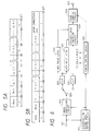
- Fig. 1 is a schematic block diagram of an image information transmitting system as a prior art.
- the image information transmitting system includes an input terminal 301.
- An analog signal obtained by raster-scanning, e.g., a television signal is sampled at a predetermined frequency, and data (n bits/sample) is input to the input terminal 301.
- the digital image data having 2 n gradation levels are supplied to a pixel block dividing circuit 302.
- Fig. 2 is a view showing a state wherein one-frame pixel data are divided into pixel blocks.
- the one-frame pixel data are temporarily stored in a memory or the like.
- the pixel data are read out in units of blocks each having (l x m) pixels, i.e., l pixels in the horizontal direction (to be referred to as an H direction hereinafter) and m pixels in the vertical direction (to be referred to as a V direction thereinafter). That is, the data are output in units of pixel blocks.
- Fig. 3 shows a format of each pixel block.
- This pixel block contains pixel data D 1,1 to D m,l .
- Image data output from the pixel block dividing circuit 302 are input to a MAX value detection circuit 303, a MIN value detection circuit 304, and a timing adjusting circuit 305.
- a pixel (D max ) having a MAX value and a pixel (D min ) having a MIN value are detected by and output from the detection circuits 303 and 304, respectively.
- the timing adjusting circuit 305 delays all the pixel data by a period required to cause the MAX and MIN value detection circuits 303 and 304 to detect the pixels D max and D min .
- the pixel data are sent to a divided value converting circuit 306 in units of pixel blocks in a predetermined order. For example, data are sent in an order of D 1,1 , D 2,1 , D 3,1 ,..., D m,1 , D 1,2 ,... D m,2 ,..., D 1,(l-1) ,... D m,(l-1) , D 1,l ,..., and D m,l in units of pixel blocks.
- All the pixel data (D 1,1 to D m,l ) and MAX and MIN values (D max and D min ) of each pixel block are input to the divided value converting circuit 306 and are compared with 2 k (where k is an integer smaller than n ) quantization levels between the values D max and D min , thereby obtaining k-bit division codes ( ⁇ 1,1 to ⁇ m,l ).
- the quantization state is shown in Fig. 4A.
- the division code ⁇ i,j is output as a k-bit binary code.
- the obtained k-bit division code ⁇ i,j and the n-bit values D max and D min are converted into serial data by parallel-to-serial (P-S) converters 307, 307', and 307", respectively.
- P-S parallel-to-serial
- One of the outputs from the P-S converters is selected by a data selector 308, thus obtaining serial data shown in Fig. 5A.
- the data output from the data selector 308 is added with a p-bit error correction code (Fig. 5B) by an error correction code adding circuit 309.
- the output from the error correction code adding circuit 309 is processed by a first-in first-out (FIFO) memory 310 along the time axis so as to obtain a predetermined data transmission rate.
- a synchronizing signal adding circuit 311 is added with a synchronizing signal by a synchronizing signal adding circuit 311.
- the obtained signal is sent out from an output terminal 312 onto a transmission line (a magnetic recording/reproducing system such as a VTR).
- the synchronizing signal is added in units of pixel blocks or every plurality of pixel blocks.
- the operation timings of the above circuits are determined on the basis of timing signals output from a timing control circuit 313.
- Fig. 6 is a block diagram showing a schematic arrangement of a receiving side corresponding to a data transmitting side shown in Fig. 1.
- the receiving side in Fig. 6 includes an input terminal 821 for receiving transmission data highly efficiently coded at the transmitting side.
- the input transmission signal is supplied to a synchronizing signal separating circuit 822 and an error correction circuit 823.
- the synchronizing signal separating circuit 822 separates a synchronizing signal from the input transmission data and sends the separated synchronizing signal to the error correction circuit 823 and a timing control circuit 831.
- the error correction circuit 823 separates the error correction code from the transmission data in synchronism with the synchronizing signal supplied from the synchronizing signal separating circuit 822, detects a data error generated along the transmission line in accordance with the error correction code, corrects this error, and supplies the corrected data to a data selector 824.
- the timing control circuit 831 controls operating timings of the respective circuits on the receiving side on the basis of the synchronizing signal supplied from the synchronizing signal separating circuit 822.
- the data selector 824 separates the transmission data into the n-bit data D max and D min and the k-bit codes ⁇ i,j quantized between the values D max and D min . These separated data are supplied to serial-to-parallel (S-P) converters 825 and 825', respectively, and are converted into parallel data thereby.
- S-P serial-to-parallel
- the MAX and MIN value data D max and D min converted into the parallel data by the S-P converter 825 are latched by latch circuits 826 and 827, respectively.
- the latched MAX and MIN value data D max and D min are supplied to a divided value inverting circuit 828.
- the division code ⁇ i,j associated with all the pixel data in each pixel block are output from the S-P converter 825' in a predetermined order and are supplied to the divided value inverting converter 828.
- Fig. 4B is a view showing a state wherein representation data D i,j ' associated with the original pixel data are decoded from the division code ⁇ i,j and the MAX and MIN value data D max and D min .
- the representation value is set to be an intermediate value between the adjacent ones of 2 k quantization levels between the values D max and D min .
- the resultant n-bit representation value data (D 1,1 ' to D m,l ') from the divided value inverting circuit 828 are output in units of pixel blocks in the predetermined order.
- output data from the divided value inverting circuit 828 is converted in an order corresponding to raster scan, and the obtained data appears as decoded image data at an output terminal 830.
- the error correction code in order to correct a data error occurring on the transmission line, the error correction code must be added to the transmission data at the transmitting side, and the obtained data is sent onto the transmission line. At the receiving side, the data error occurring on the transmission line is corrected by using the error correction code. Redundancy of the transmission data is increased by the error correction code, and transmission efficiency cannot be improved much.
- the invention provides a method of transmitting image information, comprising:
- Embodiments of the invention illustrate various techniques for the replacing of erroneous data, such that image degradation can be minimised.
- the invention further provides a transmitting apparatus and a receiving apparatus suitable for implementing respective parts of the method of the invention, and also provides an image signal conveying image information transmitted in accordance with that method.
- Fig. 7A shows a schematic arrangement of a transmitting side of an image information transmitting system according to the first embodiment of the present invention.
- the same reference numerals as in Fig. 1 denote the same parts in Fig. 7A, and a detailed description thereof will be omitted.
- an error detection code adding circuit 101 adds q- and r-bit error detection codes to serial data output from a data selector 308a, and the obtained data are supplied to a FIFO memory 310, as shown in Fig. 7B.
- the error detection codes added by the error detection code adding circuit 101 are used to detect whether an error occurs in data.
- the number of bits of the error detection codes can be smaller than that of the error correction code, and redundancy of the transmission data can be reduced.
- Fig. 8 shows a schematic arrangement of a receiving side of the image information transmitting system according to the first embodiment of the present invention.
- the receiving side includes an input terminal 201 for receiving transmission data (Fig. 7B) coded with high efficiency by the transmitting side of Fig. 7A.
- the input transmission data is supplied to a data selector 202, an error detection circuit 203, and a synchronizing signal separating circuit 204.
- synchronizing signal separating circuit 204 a synchronizing signal is separated from the input transmission data, and the separated synchronizing signal is supplied to the error detection circuit 203 and a timing control circuit 205.
- the timing control circuit 205 controls operation timings of the respective circuits in the receiving side on the basis of the synchronizing signal supplied from the synchronizing signal separating circuit 204.
- the data selector 202 supplies the n-bit data D max to the A side, the n-bit data D min to the B side, and the k-bit code ⁇ i,j obtained by quantizing the data between the data D max and D min to the C side. These data are converted by serial-to-parallel (S-P) converters 206a, 206b, and 206c into parallel data, respectively.
- S-P serial-to-parallel
- the MAX value data D max of each pixel block which is converted into the parallel data by the S-P converter 206a is supplied to a memory 207a, and the B terminal of a data selector 208a.
- the MIN value data D min of each pixel block which is converted into the parallel data by the S-P converter 206b is supplied to a memory 207b and the B terminal of a data selector 208b.
- the division code ⁇ i,j associated with each pixel data within each pixel block and converted into the parallel data by the S-P converter 206c is supplied to a memory 207c and the B terminal of a data selector 208c.
- the memories 207a, 207b, and 207c are used to delay the input data by a one-field period each.
- the A terminals of the data selectors 208a, 208b, and 208c receive the MAX value data D max , the MIN value data D min , and the division code ⁇ i,j , respectively, of the immediately preceding field period.
- switching of the data selectors 208a, 208b, and 208c is controlled by an error detection result output from the error detection circuit 203. More specifically, when the error detection circuit 203 detects that no error occurs in the transmission data, the data selectors 208a to 208c are connected to the corresponding B terminals.
- the data selectors 208a and 208b are connected to the A terminals, respectively, and the data selector 208c is connected to the B terminal.
- the division code ⁇ i,j has an error, all the data selectors 208a to 208c are connected to the A side.
- the interpolation data is output from the data selector 208a, the data selector 208b, and/or the data selector 208c.
- the MAX value data D max , the MIN value data D min , and the division code ⁇ i,j respectively output from the data selectors 208a, 208b, and 208c are supplied to a divided value inverting circuit 211.
- the divided value inverting circuit 211 decodes the n-bit representation data D i,j associated with the original pixel data on the basis of the division code ⁇ i,j and the data D max and D min as in the receiving side shown in Fig. 6.
- the decoded data is supplied to a scan convert circuit 212.
- the scan convert circuit 212 converts the output data from the divided value inverting circuit 211 in an order corresponding to raster scan, and the converted data is output as decoded image data from an output terminal 213.
- the image data can be transmitted without its degradation.
- the transmission data of an immediately preceding field period stored in the memories 207a, 207b, and 207c can be transmitted to the divided value inverting circuit 211 as interpolation data in place of the data having the error.
- the present invention is not limited to this scheme.
- the transmission data of an immediately preceding field period, of transmission data which corresponds to an error, and transmission data corresponding to neighboring pixel blocks of a pixel block represented by the transmission data of the immediately preceding field period may be used to calculate interpolation data. With this arrangement, degradation of the image data can be minimized.
- Fig. 9A shows a schematic arrangement of a transmitting side of an image information transmitting system according to the second embodiment of the present invention.
- the same reference numerals as in Fig. 1 denote the same parts in Fig. 9A, and a detailed description thereof will be omitted.
- an error detection code adding circuit 101 adds q- and r-bit error detection codes to serial data output from a data selector 308a, and the obtained data are supplied to a FIFO memory 310, as shown in Fig. 9B.
- the error detection codes added by the error detection code adding circuit 101 are used to detect whether an error occurs in data.
- the number of bits of the error detection codes can be smaller than that of the error correction code, and redundancy of the transmission data can be reduced.
- Fig. 10 shows a schematic arrangement of a receiving side of the image information transmitting system according to the second embodiment of the present invention.
- the receiving side includes an input terminal 1201 for receiving transmission data (Fig. 9B) coded with high efficiency by the transmitting side of Fig. 9A.
- the input transmission data is supplied to memories 1202 and 1203, an error detection circuit 1204, and a synchronizing signal separating circuit 1205.
- the synchronizing signal separating circuit 1205 separates a synchronizing signal from the input transmission data and supplies the synchronizing signal to the error detection circuit 1204 and a timing control circuit 1217.
- the timing control circuit 1217 controls operation timings of the respective circuits on the receiving side on the basis of the synchronizing signal supplied from the synchronizing signal separating circuit 1205.
- the transmission data input from the input terminal 1201 are sequentially stored in the memories 1202 and 1203.
- the error detection circuit 1204 outputs error detection data representing that one of MAX value data D max , MIN value data D min , and a division code ⁇ i,j in the transmission data input from the input terminal 1201 has an error.
- the error detection data output from the error detection circuit 1204 is stored in an error detection data memory 1206.
- the transmission data corresponding to one-field image data is stored in the memories 1202 and 1203, and the error detection data corresponding to this transmission data is stored in the error detection data memory 1206.
- the data stored in the respective memories are then read out.
- new input transmission data and new error detection data are stored in the corresponding memory. Therefore, the memories store the new data in place of the readout data.
- the transmission data stored in the memory 1203 is read out in a FIFO order and supplied to the B terminal of a data selector 1207.
- an address generating circuit 1208 When the MAX value data D max or the MIN value data D min has an error, an address generating circuit 1208 outputs to the memory 1202 an address for reading out the data D max or D min in the transmission data corresponding to the neighboring pixel blocks on the screen in response to the error detection data supplied from the error detection data memory 1206.
- the address generating circuit 1208 When the division code ⁇ i,j has an error, the address generating circuit 1208 outputs to the memory 1202 an address for reading out the codes ⁇ i,j corresponding to the neighboring pixels in the pixel block.
- the stored data are read out from the memory 1202 in response to the read address output from the address generating circuit 1208.
- the readout data is supplied to an operation circuit 1209.
- the operation circuit 1209 calculates interpolation MAX value data D max ', interpolation MIN value data D min ', and an interpolation division code ⁇ i,j ' by using the data supplied from the memory 1202. The calculated data are supplied to the A terminal of the data selector 1207.
- the error detection data read out from the error detection data memory 1206 is also supplied to a data selector control circuit 1210.
- the data selector control circuit 1210 connects the data selector 1207 to the A terminal. Otherwise, the data selector control circuit 1210 connects the data selector 1207 to the B terminal.
- the data having an error is replaced with the corresponding interpolation data, and the interpolated data is output.
- the transmission data output from the data selector 1207 is separated into n-bit data D max and D min and the division code ⁇ i,j by a data selector 1211. These separated data are converted into parallel data by serial-to-parallel (S-P) converters 1212 and 1213.
- S-P serial-to-parallel
- the parallel MAX and MIN value data D max and D min from the S-P converter 1212 are latched by latches 1214 and 1215, respectively.
- the latched MAX and MIN value data D max and D min are supplied to a divided value inverting circuit 1216.
- the division code ⁇ i,j converted as parallel data by the S-P converter 1213 is also supplied to the divided value inverting circuit 1216.
- the divided value inverting circuit 1216 decodes n-bit representation data D i,j ' associated with the original pixel data on the basis of the division code ⁇ i,j and the data D max and D min as in the receiving side shown in Fig. 6.
- the decoded value is supplied to a scan convert circuit 1218.
- the scan convert circuit 1218 converts the output data from the divided value inverting circuit 1216 in an order corresponding to raster scan.
- the converted data is output as decoded image data from an output terminal 1219.
- the image data can be corrected to an extent that image quality degradation occurring on the transmission line is negligible. Since extra data is not transmitted, transmission efficiency can be improved.
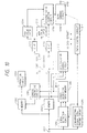
- Fig. 11A shows a schematic arrangement of a transmitting side of an image information transmitting system according to the third embodiment of the present invention.
- the same reference numerals as in Fig. 1 denote the same parts in Fig. 11A, and a detailed description thereof will be omitted.
- an error detection code adding circuit 101 adds q- and r-bit error detection codes to serial data output from a data selector 308a, and the obtained data are supplied to a FIFO memory 310, as shown in Fig. 11B.
- the error detection codes added by the error detection code adding circuit 101 are used to detect whether an error occurs in data.
- the number of bits of the error detection codes can be smaller than that of the error correction code, and redundancy of the transmission data can be reduced.
- Fig. 12 shows a schematic arrangement of a receiving side of the image information transmitting system according to the third embodiment of the present invention.
- the receiving side includes an input terminal 2201 for receiving transmission data (Fig. 11B) coded with high efficiency by the transmitting side of Fig. 11A.
- the input transmission data is supplied to a data selector 2202, an error detection circuit 2203, and a synchronizing signal separating circuit 2204.
- synchronizing signal separating circuit 2204 a synchronizing signal is separated from the input transmission data, and the separated synchronizing signal is supplied to the error detection circuit 2203 and a timing control circuit 2205.
- the timing control circuit 2205 controls operation timings of the respective circuits in the receiving side on the basis of the synchronizing signal supplied from the synchronizing signal separating circuit 2204.
- the data selector 2202 supplies the n-bit data D max to the A side, the n-bit data D min to the B side, and the k-bit code ⁇ i,j obtained by quantizing the data between the data D max and D min to the C side. These data are converted by serial-to-parallel (S-P) converters 2206a, 2206b, and 2206c into parallel data, respectively.
- S-P serial-to-parallel
- the MAX value data D max of each pixel block which is converted into the parallel data by the S-P converter 2206a is supplied to a memory 2207a and the B terminal of a data selector 2208a.
- the MIN value data D min of each pixel block which is converted into the parallel data by the S-P converter 2206b is supplied to a memory 2207b and the B terminal of a data selector 2208b.
- the division code ⁇ i,j associated with each pixel data within each pixel block and converted into the parallel data by the S-P converter 2206c is supplied to a memory 2207c, the B terminal of a data selector 2208c, and an operation circuit 2209.
- the memories 2207a, 2207b, and 2207c are used to delay the input data by a one-field period each.
- the A terminals of the data selectors 2208a, 2208b, and 2208c receive the MAX value data D max , the MIN value data D min , and the division code ⁇ i,j , respectively.
- the operation circuit 2209 is a circuit for calculating an average value of the division codes ⁇ i,j associated with the pixel data of the pixel blocks output from the S-P converter 2206c.
- the data calculated by the operation circuit 2209 is supplied to the C terminal of the data selector 2208c, and a fixed data generator 2210 generates data representing an intermediate value of the values represented by the division codes ⁇ i,j .
- the output from the fixed data generator 2210 is supplied to the D terminal of the data selector 2208c.
- switching of the data selectors 2208a, 2208b, and 2208c is controlled by an error detection result output from the error detection circuit 2203. More specifically, when the error detection circuit 2203 detects that no error occurs in the transmission data, the data selectors 2208a to 2208c are connected to the corresponding B terminals. When only the MAX value data D max has an error, the data selector 2208a is connected to the A terminal. When only the MIN value data D min has an error, the data selector 2208b is connected to the A terminal. When the MIN and MIN value data D max and D min and the division code ⁇ i,j have errors, all the data selectors 2208a to 2208c are connected to the A side.
- the data selector 2208c when no error is present in the MAX data D max and the MIN value data D min , and an error is present in the division code ⁇ i,j , the data selector 2208c is connected to the C or D terminal in accordance with an error rate. More specifically, when the error detection circuit 2203 detects that the number of errors in the division codes ⁇ i,j exceeds a predetermined number, the average value of the division codes ⁇ i,j cannot be calculated. In this case, the data selector 2208c is connected to the D terminal, and data representing an intermediate value of the values of the division codes ⁇ i,j is output from the data selector 2208c in place of the data representing the average value.
- the error detection circuit 2203 detects that the detected number of errors in the division codes ⁇ i,j is smaller than the predetermined number
- the data selector 2208c is connected to the C terminal.
- Data representing the average value of the division codes ⁇ i,j and calculated by the operation circuit 2209 is output from the data selector 2208c.
- the data selectors 2208a, 2208b, and 2208c output the corresponding interpolation data in place of the error data.
- the MAX value data D max , the MIN value data D min , and the division code ⁇ i,j respectively output from the data selectors 2208a, 2208b, and 2208c are supplied to a divided value inverting circuit 2211.
- the divided value inverting circuit 2211 decodes n-bit representation value data D i,j associated from the original pixel data on the basis of the division code ⁇ i,j and the data D max and D min as in the receiving side shown in Fig. 6.
- the decoded data is supplied to a scan convert circuit 2212.
- the scan convert circuit 2211 converts the output data from the divided value inverting circuit 2211 in an order corresponding to raster scan.
- the converted data is output as decoded image data from an output terminal 2213.
Landscapes
- Engineering & Computer Science (AREA)
- Multimedia (AREA)
- Signal Processing (AREA)
- Compression Or Coding Systems Of Tv Signals (AREA)
- Detection And Prevention Of Errors In Transmission (AREA)
Claims (14)
- Verfahren zum Übertragen von Bildinformation, mit den Verfahrensschritten:(a) Einteilen (302) einer Vielzahl von ein Bild zusammenfassenden Pixeldaten in eine Vielzahl von Pixeldatenblöcken, wobei jeder Block eine vorbestimmte Anzahl (1 × m) von Pixeln umfaßt;(b) Formieren (304 - 306) von Aufteilungsdaten (Dmin, Dmax) für jeden Pixeldatenblock, die eine Aufteilung der Pixeldaten des Pixeldatenblockes repräsentieren, und von Positionsdaten (Δi, j), die für jedes Pixel des Blockes eine relative Position in der Aufteilung darstellen, die durch die Aufteilungsdaten repräsentiert ist;(c) Senden (307 - 312) für jeden Block über einen Übertragungskanal: (i) die Aufteilungsdaten; (ii) die Positionsdaten und (iii) Fehlerfeststelldaten zur Verwendung bei der Feststellung, ob ein Fehler im Übertragungskanal aufgetreten ist;(d) Empfangen (201 - 206) der Aufteilungsdaten, der Positionsdaten und der Fehlerfeststelldaten, die für jeden Block über den Übertragungskanal gesendet wurden;(e) Feststellen (203), ob ein Fehler in den Empfangsdaten für einen vorgegebenen Block unter Verwendung der empfangenen Fehlerfeststelldaten aufgetreten ist; und(f) Ersetzen (208a - 208c) festgestellter fehlerhafter Daten der empfangenen Daten unter Verwendung anderer Daten (a) abhängig von der Feststellung des Fehlerauftritts;wobei der Verfahrensschritt der Feststellung (e) für jeden Block zwischen Fehlern unterscheidet, die in den Aufteilungsdaten auftreten, und Fehlern, die in den Positionsdaten auftreten, wobei der Verfahrensschritt des Ersetzens (f) in einer Weise ausgeführt wird, die vom Ergebnis der Unterscheidung abhängt, und wobei die Fehlerfeststelldaten für die Feststellung, nicht jedoch für die Korrektur von in den Aufteilungsdaten und den Positionsdaten aufgetretenen Fehlern hinreichend sind.
- Verfahren nach Anspruch 1, bei dem für den Verfahrensschritt (f) vorhergehend gesendete und empfangene Daten über den Übertragungskanal als die anderen Daten verwendet werden.
- Verfahren nach Anspruch 1 oder 2, bei dem für den Verfahrensschritt (f) die für das Ersetzen der fehlerhaften Daten eines vorgegebenen Blockes verwendeten anderen Daten solche enthält, die in Hinsicht auf dasselbe Bild, das den vorgegebenen Block einschließt, über den Übertragungskanal gesendet und empfangen wurden.
- Verfahren nach Anspruch 1 oder 2, bei dem für den Verfahrensschritt (f) die zum Ersetzen fehlerhaften Daten eines vorgegebenen Blockes verwendeten anderen Daten solche einschließt, die in Hinsicht auf ein anderes Bild als das, das den vorgegebenen Block enthält, über den Übertragungskanal gesendet und empfangen wurden.
- Verfahren nach einem der vorstehenden Ansprüche, bei dem für einen Block mit einem Fehler, der nur in den Aufteilungsdaten festgestellt wurde, die fehlerhaften Aufteilungsdaten unter Verwendung der anderen Daten ersetzt werden, während die empfangenen Positionsdaten nicht ersetzt werden.
- Verfahren nach einem der vorstehenden Ansprüche, bei dem die Positionsdaten durch vorbestimmte Daten ersetzt werden, die eine Zwischenposition in der Aufteilung darstellen, wenn kein Fehler in den empfangenen Aufteilungsdaten festgestellt wird, während Fehler über einer vorbestimmten Anzahl in den Positionsdaten für den Block auftreten.
- Verfahren nach einem der vorstehenden Ansprüche, bei dem fehlerhafte Positionsdaten unter Verwendung eines Durchschnittswertes der für den Block empfangenen Positionsdaten ersetzt werden, wenn in den empfangenen Positionsdaten festgestellte Fehler für einen Block eine vorbestimmte Anzahl nicht übersteigen.
- Verfahren nach einem der vorstehenden Ansprüche, bei dem für einen Block mit Fehlern in den Aufteilungsdaten und den Positionsdaten die gesamten Daten für diesen Block ersetzt werden.
- Verfahren nach einem der vorstehenden Ansprüche, bei dem die Aufteilungsdaten zwei Komponenten umfassen, die einen Dynamikbereich von Pixelwerten für jeden Block definieren, und bei dem Fehler festgestellt werden und das Ersetzen für die individuellen Komponenten der Aufteilungsdaten ausgeführt wird.
- Gerät zum Tragen von Bildinformation über einen Übertragungskanal, mit:Mitteln (302) zum Einteilen einer Vielzahl von ein Bild zusammenfassenden Pixeldaten in eine Vielzahl von Pixeldatenblöcken, wobei jeder Block eine vorbestimmte Anzahl von Pixeln darstellt;Mitteln (304 - 306) zum Formieren von Aufteilungsdaten (Dmin, Dmax) für jeden Pixeldatenblock, die eine Aufteilung der Pixeldaten des Pixeldatenblockes repräsentieren, und von Positionsdaten (Δi, j), die für jedes Pixel des Blockes eine relative Position in der Aufteilung darstellen, die durch die Aufteilungsdaten repräsentiert ist; und mitMitteln (307 - 312) zum Senden für jeden Block über einen Übertragungskanal: (i) die Aufteilungsdaten; (ii) die Positionsdaten und (iii) Fehlerfeststelldaten zur Verwendung bei der Feststellung, ob ein Fehler im Übertragungskanal aufgetreten ist;wobei die Fehlerfeststelldaten so erzeugt werden, daß sie die Unterscheidung für einen vorgegebenen Block unter Fehlern gestatten, die in den Aufteilungsdaten auftreten und Fehlern, die in den Positionsdaten auftreten,dadurch gekennzeichnet, daß die Fehlerfeststelldaten für die Feststellung, nicht jedoch für die Korrektur von in den Aufteilungsdaten und den Positionsdaten aufgetretenen Fehlern hinreichend sind.
- Sendegerät nach Anspruch 10, bei dem die Aufteilungsdaten zwei Komponenten umfassen, die einen Dynamikbereich für Pixeldaten des Blockes festlegen, und bei dem die Fehlerfeststelldaten so erzeugt werden, daß sie die Unterscheidung zwischen den Fehlern bei der Sendung einer jeden Komponente gestattet.
- Gerät zum Empfang von Bildinformation über einen Übertragungskanal, bei dem Pixeldaten für ein Bild zur Sendung in eine Vielzahl von Pixeldatenblöcken eingeteilt sind, wobei jeder Block eine vorbestimmte Anzahl von Pixeln repräsentiert, mit:Mitteln (201 - 206) für jeden Block zum Empfang von: (i) Aufteilungsdaten, die eine Aufteilung der Pixeldaten des Blockes darstellen; (ii) Positionsdaten, die für jedes Pixel des Blockes eine relative Position in der Aufteilung darstellen, die durch die Aufteilungsdaten dargestellt wird; und (iii) Fehlerfeststelldaten;einem Mittel (203) zur Feststellung unter Verwendung der empfangenen Fehlerfeststelldaten, ob ein Fehler in den empfangenen Daten für einen Block aufgetreten ist; und mitMitteln (208a - 208c) zum Ersetzen festgestellter fehlerhafter Daten der empfangenen Daten unter Verwendung anderer Daten in Abhängigkeit von der Feststellung des Auftretens des Fehlers durch das Feststellmittel,wobei das Feststellmittel (203) Mittel zur Unterscheidung für einen vorgegebenen Block zwischen in den Aufteilungsdaten auftretenden Fehlern und in den Positionsdaten auftretenden Fehlern enthält, und wobei die Fehlerfeststelldaten, die mit den Aufteilungsdaten und den Positionsdaten empfangen werden, hinreichend sind zur Feststellung, aber nicht zur Korrektur der in den Aufteilungsdaten und den Positionsdaten auftretenden Fehler.
- Empfangsgerät nach Anspruch 12, dessen Aufteilungsdaten zwei Komponenten umfassen, die einen Dynamikbereich für die Pixeldaten jeden Blockes festlegen, und wobei das Feststellmittel (203) Mittel zur Unterscheidung zwischen Fehlern bei der Sendung jeder der individuellen Komponenten enthält.
- Signaltransportierende Bildinformation, bei der eine Vielzahl von Pixeldaten ein Bild zusammenfassen, die in eine Vielzahl von Pixeldatenblöcken eingeteilt sind, wobei der Signaltransport für jedes der Blockaufteilungsdaten die Aufteilung von Pixeldaten des Pixeldatenblockes und Positionsdaten repräsentiert, die für jedes Pixel des Blockes eine relative Position in der durch die Aufteilungsdaten repräsentierten Aufteilung darstellen, wobei das Signal Fehlerfeststelldaten für jeden Block transportiert, die die Unterscheidung zwischen Fehlern gestatten, die in den Aufteilungsdaten auftreten, und Fehlern, die in den Positionsdaten auftreten, dadurch gekennzeichnet, daß die Fehlerfeststelldaten hinreichend sind zur Feststellung, nicht aber zur Korrektur von in den Aufteilungsdaten und den Positionsdaten auftretenden Fehlern.
Applications Claiming Priority (6)
| Application Number | Priority Date | Filing Date | Title |
|---|---|---|---|
| JP126381/89 | 1989-05-19 | ||
| JP1126380A JPH02305281A (ja) | 1989-05-19 | 1989-05-19 | 画像情報伝送方式 |
| JP126380/89 | 1989-05-19 | ||
| JP1126381A JPH02305282A (ja) | 1989-05-19 | 1989-05-19 | 画像情報伝送方式 |
| JP126379/89 | 1989-05-19 | ||
| JP12637989A JP2951967B2 (ja) | 1989-05-19 | 1989-05-19 | 画像復号化方法及びその装置 |
Publications (3)
| Publication Number | Publication Date |
|---|---|
| EP0398741A2 EP0398741A2 (de) | 1990-11-22 |
| EP0398741A3 EP0398741A3 (de) | 1991-08-28 |
| EP0398741B1 true EP0398741B1 (de) | 1997-10-29 |
Family
ID=27315318
Family Applications (1)
| Application Number | Title | Priority Date | Filing Date |
|---|---|---|---|
| EP90305399A Expired - Lifetime EP0398741B1 (de) | 1989-05-19 | 1990-05-18 | System zum Übertragen von Bildinformation |
Country Status (3)
| Country | Link |
|---|---|
| US (1) | US5448298A (de) |
| EP (1) | EP0398741B1 (de) |
| DE (1) | DE69031638T2 (de) |
Cited By (8)
| Publication number | Priority date | Publication date | Assignee | Title |
|---|---|---|---|---|
| US6351494B1 (en) | 1999-09-24 | 2002-02-26 | Sony Corporation | Classified adaptive error recovery method and apparatus |
| US6389562B1 (en) | 1999-06-29 | 2002-05-14 | Sony Corporation | Source code shuffling to provide for robust error recovery |
| US6473876B1 (en) | 1999-06-29 | 2002-10-29 | Sony Corporation | Method and apparatus for encoding of bitstreams using rotation |
| US6493842B1 (en) | 1999-06-29 | 2002-12-10 | Sony Corporation | Time-varying randomization for data synchronization and implicit information transmission |
| US6519369B1 (en) | 1999-02-12 | 2003-02-11 | Sony Corporation | Method and apparatus for filter tap expansion |
| US6522785B1 (en) | 1999-09-24 | 2003-02-18 | Sony Corporation | Classified adaptive error recovery method and apparatus |
| US6539517B1 (en) | 1999-11-09 | 2003-03-25 | Sony Corporation | Data transformation for explicit transmission of control information |
| US6621936B1 (en) | 1999-02-12 | 2003-09-16 | Sony Corporation | Method and apparatus for spatial class reduction |
Families Citing this family (17)
| Publication number | Priority date | Publication date | Assignee | Title |
|---|---|---|---|---|
| US5146325A (en) * | 1991-04-29 | 1992-09-08 | Rca Thomson Licensing Corporation | Video signal decompression apparatus for independently compressed even and odd field data |
| JP3259428B2 (ja) * | 1993-03-24 | 2002-02-25 | ソニー株式会社 | ディジタル画像信号のコンシール装置及び方法 |
| DE69428722T2 (de) * | 1993-03-31 | 2002-06-20 | Sony Corp., Tokio/Tokyo | Signalverarbeitungsanlage |
| US6377628B1 (en) | 1996-12-18 | 2002-04-23 | Thomson Licensing S.A. | System for maintaining datastream continuity in the presence of disrupted source data |
| EP0945022B1 (de) * | 1996-12-18 | 2003-02-26 | Thomson Consumer Electronics, Inc. | Effiziente kompression und dekompression von blocks fester länge |
| CN1219255C (zh) * | 1997-10-23 | 2005-09-14 | 索尼电子有限公司 | 差错恢复的设备与方法 |
| US6282684B1 (en) | 1997-10-23 | 2001-08-28 | Sony Corporation | Apparatus and method for recovery of data in a lossy transmission environment |
| US6581170B1 (en) | 1997-10-23 | 2003-06-17 | Sony Corporation | Source coding to provide for robust error recovery during transmission losses |
| US6298085B1 (en) | 1997-10-23 | 2001-10-02 | Sony Corporation | Source encoding using shuffling of data to provide robust error recovery in a burst error-environment |
| US6418548B1 (en) | 1999-02-12 | 2002-07-09 | Sony Corporation | Method and apparatus for preprocessing for peripheral erroneous data |
| US6591398B1 (en) | 1999-02-12 | 2003-07-08 | Sony Corporation | Multiple processing system |
| US6363118B1 (en) | 1999-02-12 | 2002-03-26 | Sony Corporation | Apparatus and method for the recovery of compression constants in the encoded domain |
| US6535148B1 (en) | 1999-02-12 | 2003-03-18 | Sony Corporation | Method and apparatus for truncated decoding |
| US6170074B1 (en) | 1999-02-12 | 2001-01-02 | Sony Corporation | Source coding to provide for robust error recovery |
| EP1151615B1 (de) * | 1999-02-12 | 2011-11-09 | Sony Electronics, Inc. | Vorrichtung und verfahren zur zurückgewinnung von kompressionskonstanten im kodierten bereich |
| US6307560B1 (en) | 1999-02-12 | 2001-10-23 | Sony Corporation | Classified adaptive spatio-temporal format conversion method and apparatus |
| US6549672B1 (en) | 1999-06-29 | 2003-04-15 | Sony Corporation | Method and apparatus for recovery of encoded data using central value |
Family Cites Families (14)
| Publication number | Priority date | Publication date | Assignee | Title |
|---|---|---|---|---|
| JPS5529482B2 (de) * | 1974-04-01 | 1980-08-04 | ||
| JPS5657374A (en) * | 1979-10-16 | 1981-05-19 | Sony Corp | Processor of digital video signal |
| CA1251555A (en) * | 1984-12-19 | 1989-03-21 | Tetsujiro Kondo | High efficiency technique for coding a digital video signal |
| JP2670259B2 (ja) * | 1985-11-29 | 1997-10-29 | ソニー株式会社 | 高能率符号化装置 |
| US4792953A (en) * | 1986-03-28 | 1988-12-20 | Ampex Corporation | Digital signal error concealment |
| JP2540809B2 (ja) * | 1986-07-30 | 1996-10-09 | ソニー株式会社 | 高能率符号化装置 |
| JP2508439B2 (ja) * | 1987-05-29 | 1996-06-19 | ソニー株式会社 | 高能率符号化装置 |
| US4953019A (en) * | 1987-11-27 | 1990-08-28 | Canon Kabushiki Kaisha | Image signal encoding apparatus |
| JP2629238B2 (ja) * | 1988-02-05 | 1997-07-09 | ソニー株式会社 | 復号装置及び復号方法 |
| US4903124A (en) * | 1988-03-17 | 1990-02-20 | Canon Kabushiki Kaisha | Image information signal transmission apparatus |
| US4953023A (en) * | 1988-09-29 | 1990-08-28 | Sony Corporation | Coding apparatus for encoding and compressing video data |
| US4947249A (en) * | 1988-10-14 | 1990-08-07 | Sony Corporation | Apparatus in which subsampling and block coding are both employed for coding digital video data |
| US5150210A (en) * | 1988-12-26 | 1992-09-22 | Canon Kabushiki Kaisha | Image signal restoring apparatus |
| US5122876A (en) * | 1988-12-26 | 1992-06-16 | Canon Kabushiki Kaisha | Image signal restoring apparatus |
-
1990
- 1990-05-18 DE DE69031638T patent/DE69031638T2/de not_active Expired - Fee Related
- 1990-05-18 EP EP90305399A patent/EP0398741B1/de not_active Expired - Lifetime
-
1994
- 1994-11-10 US US08/338,815 patent/US5448298A/en not_active Expired - Fee Related
Cited By (9)
| Publication number | Priority date | Publication date | Assignee | Title |
|---|---|---|---|---|
| US6519369B1 (en) | 1999-02-12 | 2003-02-11 | Sony Corporation | Method and apparatus for filter tap expansion |
| US6621936B1 (en) | 1999-02-12 | 2003-09-16 | Sony Corporation | Method and apparatus for spatial class reduction |
| US6389562B1 (en) | 1999-06-29 | 2002-05-14 | Sony Corporation | Source code shuffling to provide for robust error recovery |
| US6473876B1 (en) | 1999-06-29 | 2002-10-29 | Sony Corporation | Method and apparatus for encoding of bitstreams using rotation |
| US6493842B1 (en) | 1999-06-29 | 2002-12-10 | Sony Corporation | Time-varying randomization for data synchronization and implicit information transmission |
| US6553381B2 (en) | 1999-06-29 | 2003-04-22 | Sony Corporation | Time-varying randomization for data synchronization and implicit information transmission |
| US6351494B1 (en) | 1999-09-24 | 2002-02-26 | Sony Corporation | Classified adaptive error recovery method and apparatus |
| US6522785B1 (en) | 1999-09-24 | 2003-02-18 | Sony Corporation | Classified adaptive error recovery method and apparatus |
| US6539517B1 (en) | 1999-11-09 | 2003-03-25 | Sony Corporation | Data transformation for explicit transmission of control information |
Also Published As
| Publication number | Publication date |
|---|---|
| DE69031638D1 (de) | 1997-12-04 |
| US5448298A (en) | 1995-09-05 |
| EP0398741A2 (de) | 1990-11-22 |
| DE69031638T2 (de) | 1998-03-19 |
| EP0398741A3 (de) | 1991-08-28 |
Similar Documents
| Publication | Publication Date | Title |
|---|---|---|
| EP0398741B1 (de) | System zum Übertragen von Bildinformation | |
| US4217609A (en) | Adaptive predictive coding system for television signals | |
| US5193003A (en) | Apparatus for decoding digital video data with small memory requirement | |
| EP0473384A2 (de) | Kodierungsgerät für digitale Bildsignale | |
| EP0138529A2 (de) | Adaptierende Vorhersage von Bilddaten | |
| US4910594A (en) | Method and apparatus for adaptively compressing a video signal in accordance with the valves of individual pixels | |
| EP0539155B1 (de) | Verfahren zur Bildübertragung | |
| JPS5989086A (ja) | 画像デ−タ伝送方式 | |
| US5532837A (en) | Digital video signal processing apparatus | |
| US4982270A (en) | Video data transmitting system | |
| US5040060A (en) | Image information transmission system with compression based on still-image redundancy | |
| EP0891101B1 (de) | Vorrichtung und verfahren zur bildkodierung und -dekodierung sowie aufzeichnungsmedium | |
| US5023715A (en) | Method of and apparatus for transmitting image information | |
| US6339615B1 (en) | Picture encoding device, picture encoding method, picture decoding device, picture decoding method, and recording medium | |
| US4677621A (en) | Signal storage system | |
| US5047854A (en) | Image information transmission system transmitting maximum and minimum value data | |
| EP0699001A2 (de) | Verfahren zur Komprimierung/Übertragung von Bilddatensignalen | |
| EP0390471B1 (de) | Vorhersage-Kodierungsvorrichtung | |
| US6731816B2 (en) | Image processing apparatus | |
| JP2951967B2 (ja) | 画像復号化方法及びその装置 | |
| JP2888523B2 (ja) | 画像処理装置 | |
| JP3271109B2 (ja) | ディジタル画像信号処理装置および処理方法 | |
| JPH0133993B2 (de) | ||
| JP2692899B2 (ja) | 画像符号化装置 | |
| JP3040728B2 (ja) | 画像処理装置および画像処理方法 |
Legal Events
| Date | Code | Title | Description |
|---|---|---|---|
| PUAI | Public reference made under article 153(3) epc to a published international application that has entered the european phase |
Free format text: ORIGINAL CODE: 0009012 |
|
| AK | Designated contracting states |
Kind code of ref document: A2 Designated state(s): DE ES FR GB IT NL |
|
| 17P | Request for examination filed |
Effective date: 19901231 |
|
| PUAL | Search report despatched |
Free format text: ORIGINAL CODE: 0009013 |
|
| AK | Designated contracting states |
Kind code of ref document: A3 Designated state(s): DE ES FR GB IT NL |
|
| 17Q | First examination report despatched |
Effective date: 19930802 |
|
| GRAG | Despatch of communication of intention to grant |
Free format text: ORIGINAL CODE: EPIDOS AGRA |
|
| GRAH | Despatch of communication of intention to grant a patent |
Free format text: ORIGINAL CODE: EPIDOS IGRA |
|
| GRAH | Despatch of communication of intention to grant a patent |
Free format text: ORIGINAL CODE: EPIDOS IGRA |
|
| GRAA | (expected) grant |
Free format text: ORIGINAL CODE: 0009210 |
|
| AK | Designated contracting states |
Kind code of ref document: B1 Designated state(s): DE ES FR GB IT NL |
|
| PG25 | Lapsed in a contracting state [announced via postgrant information from national office to epo] |
Ref country code: ES Free format text: THE PATENT HAS BEEN ANNULLED BY A DECISION OF A NATIONAL AUTHORITY Effective date: 19971029 Ref country code: NL Free format text: LAPSE BECAUSE OF FAILURE TO SUBMIT A TRANSLATION OF THE DESCRIPTION OR TO PAY THE FEE WITHIN THE PRESCRIBED TIME-LIMIT Effective date: 19971029 Ref country code: IT Free format text: LAPSE BECAUSE OF FAILURE TO SUBMIT A TRANSLATION OF THE DESCRIPTION OR TO PAY THE FEE WITHIN THE PRESCRIBED TIME-LIMIT;WARNING: LAPSES OF ITALIAN PATENTS WITH EFFECTIVE DATE BEFORE 2007 MAY HAVE OCCURRED AT ANY TIME BEFORE 2007. THE CORRECT EFFECTIVE DATE MAY BE DIFFERENT FROM THE ONE RECORDED. Effective date: 19971029 |
|
| REF | Corresponds to: |
Ref document number: 69031638 Country of ref document: DE Date of ref document: 19971204 |
|
| ET | Fr: translation filed | ||
| NLV1 | Nl: lapsed or annulled due to failure to fulfill the requirements of art. 29p and 29m of the patents act | ||
| PLBE | No opposition filed within time limit |
Free format text: ORIGINAL CODE: 0009261 |
|
| STAA | Information on the status of an ep patent application or granted ep patent |
Free format text: STATUS: NO OPPOSITION FILED WITHIN TIME LIMIT |
|
| 26N | No opposition filed | ||
| REG | Reference to a national code |
Ref country code: GB Ref legal event code: IF02 |
|
| PGFP | Annual fee paid to national office [announced via postgrant information from national office to epo] |
Ref country code: DE Payment date: 20050720 Year of fee payment: 16 |
|
| PGFP | Annual fee paid to national office [announced via postgrant information from national office to epo] |
Ref country code: GB Payment date: 20060517 Year of fee payment: 17 |
|
| PGFP | Annual fee paid to national office [announced via postgrant information from national office to epo] |
Ref country code: FR Payment date: 20060518 Year of fee payment: 17 |
|
| PG25 | Lapsed in a contracting state [announced via postgrant information from national office to epo] |
Ref country code: DE Free format text: LAPSE BECAUSE OF NON-PAYMENT OF DUE FEES Effective date: 20061201 |
|
| GBPC | Gb: european patent ceased through non-payment of renewal fee |
Effective date: 20070518 |
|
| REG | Reference to a national code |
Ref country code: FR Ref legal event code: ST Effective date: 20080131 |
|
| PG25 | Lapsed in a contracting state [announced via postgrant information from national office to epo] |
Ref country code: GB Free format text: LAPSE BECAUSE OF NON-PAYMENT OF DUE FEES Effective date: 20070518 |
|
| PG25 | Lapsed in a contracting state [announced via postgrant information from national office to epo] |
Ref country code: FR Free format text: LAPSE BECAUSE OF NON-PAYMENT OF DUE FEES Effective date: 20070531 |