EP0398744A2 - Bi-CMOS-Logikschaltung - Google Patents
Bi-CMOS-Logikschaltung Download PDFInfo
- Publication number
- EP0398744A2 EP0398744A2 EP90305408A EP90305408A EP0398744A2 EP 0398744 A2 EP0398744 A2 EP 0398744A2 EP 90305408 A EP90305408 A EP 90305408A EP 90305408 A EP90305408 A EP 90305408A EP 0398744 A2 EP0398744 A2 EP 0398744A2
- Authority
- EP
- European Patent Office
- Prior art keywords
- mos transistor
- transistor
- mos
- logic circuit
- bipolar
- Prior art date
- Legal status (The legal status is an assumption and is not a legal conclusion. Google has not performed a legal analysis and makes no representation as to the accuracy of the status listed.)
- Withdrawn
Links
Images

Classifications
-
- H—ELECTRICITY
- H03—ELECTRONIC CIRCUITRY
- H03K—PULSE TECHNIQUE
- H03K19/00—Logic circuits, i.e. having at least two inputs acting on one output; Inverting circuits
- H03K19/01—Modifications for accelerating switching
- H03K19/013—Modifications for accelerating switching in bipolar transistor circuits
- H03K19/0136—Modifications for accelerating switching in bipolar transistor circuits by means of a pull-up or down element
-
- H—ELECTRICITY
- H03—ELECTRONIC CIRCUITRY
- H03K—PULSE TECHNIQUE
- H03K19/00—Logic circuits, i.e. having at least two inputs acting on one output; Inverting circuits
- H03K19/02—Logic circuits, i.e. having at least two inputs acting on one output; Inverting circuits using specified components
- H03K19/08—Logic circuits, i.e. having at least two inputs acting on one output; Inverting circuits using specified components using semiconductor devices
- H03K19/094—Logic circuits, i.e. having at least two inputs acting on one output; Inverting circuits using specified components using semiconductor devices using field-effect transistors
- H03K19/0944—Logic circuits, i.e. having at least two inputs acting on one output; Inverting circuits using specified components using semiconductor devices using field-effect transistors using MOSFET or insulated gate field-effect transistors, i.e. IGFET
- H03K19/09448—Logic circuits, i.e. having at least two inputs acting on one output; Inverting circuits using specified components using semiconductor devices using field-effect transistors using MOSFET or insulated gate field-effect transistors, i.e. IGFET in combination with bipolar transistors [BIMOS]
Definitions
- the present invention generally relates to a Bi-CMOS logic circuit, and more particularly to an improvement in rise and fall characteristics of an output signal from the Bi-CMOS logic circuit.
- a Bi-CMOS logic circuit is composed of a bipolar element and a CMOS (complementary metal oxide semiconductor transistor) element.
- CMOS complementary metal oxide semiconductor transistor
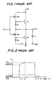
- FIG.1 there is illustrated a conventional Bi-CMOS logic circuit, which includes a CMOS inverter composed of a P-channel MOS transistor MP1 and an N-channel MOS transistor MN1 and a pair of bipolar transistors Q1 and Q2.
- the Bi-CMOS logic circuit has a high operating speed characteristic coming from the bipolar transistor pair and a low power consumption characteristic coming from the CMOS inverter.
- a resistor R1 is connected between the base and emitter of the bipolar transistor Q1 and a resistor R2 (impedance circuit) is connected between the base and emitter of the bipolar transistor Q2.
- An output terminal OUT of the Bi-CMOS logic circuit is grounded through a wiring load capacitance C, which is a parasitic capacitance.
- the bipolar transistors Q1 and Q2 are connected in series between a positive power source Vcc and a negative power source (ground).
- the output signal from the Bi-CMOS logic circuit is drawn from a connection node where the emitter of the bipolar transistor Q1 is connected to the collector of the bipolar transistor Q2.
- the MOS transistor MP1 is connected between the collector and base of the bipolar transistor Q1.
- the MOS transistor MN1 is connected between the collector and base of the bipolar transistor Q2.
- An input signal applied to an input terminal IN is supplied to the gates of the MOS transistors MP1 and MN1.
- the MOS transistor MP1 When the input signal (also indicated by IN) changes from a high (H) level (approximately equal to the power source voltage Vcc) to a low level (approximately equal to the ground potential), the MOS transistor MP1 is switched from OFF to ON. In response to this change in the state of the MOS transistor MP1, the bipolar transistor Q1 is turned ON. Thus, the load capacitance C is charged so that the output signal (also indicated by OUT) at the output terminal OUT is changed from the low level to the high level.
- the MOS transistor MP1 is switched from ON to OFF and the MOS transistor MN1 is switched from OFF to ON.
- the bipolar transistor Q2 is turned ON.
- the load capacitance C is discharged through the bipolar transistor Q2 so that the voltage of the output terminal OUT is changed from the high level to the low level.
- the bipolar transistor Q2 Until the time when the voltage of the output terminal OUT decreases to the base-emitter voltage V BE of the bipolar transistor Q2, most of current passes through the bipolar transistor Q2. This is due to the fact that the current driveability of the bipolar transistor Q2 is greater than that of the MOS transistor MN1.
- the bipolar transistor Q2 When the collector-emitter voltage of the bipolar transistor Q2 becomes equal to or less than the base-emitter voltage V BE thereof, the bipolar transistor cannot pass current. Thus, the load capacitance C is gradually discharged through the MOS transistor MN1 and the resistor R2 and finally becomes equal to the low level (approximately equal to the ground potential).
- FIG.2 is a waveform diagram of the output signal OUT obtained at the output terminal OUT.
- a letter “a” denotes the potential difference between the emitter and base of the bipolar transistor Q1
- a letter “b” denotes the potential difference between the emitter and base of the bipolar transistor Q2.
- a letter “c” denotes the time it takes the output voltage to increase by the potential difference "a”
- a letter “d” denotes the time it takes the output voltage decreases by the potential difference "b”.
- the signal waveform of the output signal OUT rises rapidly.
- the current passing the resistor R1 charges the load capacitance C so that the voltage of the output terminal OUT increases gradually by the base-emitter voltage V BE of the bipolar transistor Q1.
- the time when the current is passing through the load capacitance C is based on the time constant of R1 and C. Thus, it takes a long time the output voltage to increase to the high level so that a rounding of the waveform of the output signal appears during the time "c”.
- the current from the load capacitance C passes through the resistor R2 so that the load capacitance is gradually discharged.
- a more specific object of the present invention is to provide a Bi-CMOS logic circuit capable of providing a decreased waveform rounding and a decreased jitter.
- a Bi-CMOS logic circuit comprising first and second bipolar transistors connected in series between a first power source and a second power source, an output signal being drawn from a connection node where the first and second bipolar transistors are connected in series; a first impedance circuit connected between a base and an emitter of the first bipolar transistor; and a second impedance circuit connected between a base of the second bipolar transistor and an emitter thereof.
- the Bi-CMOS logic circuit also comprises a first MOS transistor connected between a collector of the first bipolar transistor and the base thereof; and a second MOS transistor connected between a collector of the second bipolar transistor and the base thereof. An input signal is applied to gates of the first and second MOS transistors.
- the Bi-CMOS logic circuit further comprises a third MOS transistor connected between the collector of the first bipolar transistor and the emitter thereof. The input signal is applied to a gate of the third MOS transistor. It is also possible to provide a fourth MOS transistor in place of or in addition to the third MOS transistor. The fourth MOS transistor is connected between the collector and emitter of the second bipolar transistor. The input signal is applied to the gate of the fourth MOS transistor.
- a Bi-CMOS logic circuit comprising a NAND gate connected between a first power source and a second power source, the NAND gate having first and second input terminals and an output terminal, first and second input signals being applied to the first and second input terminals, respectively; a first MOS transistor connected between the first power source and the output terminal, the first input signal being applied to a gate of the first MOS transistor; a second MOS transistor connected between the first power source and the output signal, the second input signal being applied to a gate of the second MOS transistor; a third MOS transistor; and a fourth MOS transistor, the third and fourth MOS transistors being connected in series between the output signal and the second power source, the first and second input signals being applied to gates of the third and fourth MOS transistors, respectively.
- a Bi-CMOS logic circuit comprising a NOR gate connected between a first power source and a second power source, the NAND gate having first and second input terminals and an output terminal, first and second input signals being applied to the first and second input terminals, respectively; a first MOS transistor; a second MOS transistor, the first and second MOS transistors being connected in series between the first power source and the output terminal, the first and second input terminals being applied to gates of the first and second MOS transistors, respectively; a third MOS transistor connected in series between the output terminal and the second power source, the first input signal being applied to a gate of the third MOS transistor; and a fourth MOS transistor connected in series between the output terminal and the second power source, the second input signal being applied to a gate of the fourth MOS transistor.
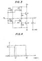
- FIG.3 A description will now be given of a Bi-CMOS logic circuit according to the first preferred embodiment of the present invention with reference to FIG.3.
- FIG.3 those parts which are the same as those shown in FIG.1 are given the same reference numerals.
- a pair of P-channel MOS transistor MP2 and N-channel MOS transistor MN2 are added to the configuration shown in FIG.1.
- the MOS transistor MP2 is connected between the collector and emitter of the bipolar transistor Q1. That is, the source and drain of the MOS transistor MP2 are connected to the collector and emitter of the bipolar transistor Q1, respectively.
- the MOS transistor MN2 is connected between the collector and emitter of the bipolar transistor Q2. That is, the drain and source of the MOS transistor MN2 are connected to the collector and emitter of the bipolar transistor Q2, respectively.
- the input signal IN through the input terminal IN is applied to the gates of the MOS transistors MP2 and MN2.
- the MOS transistors MP1 and MP2 are switched from OFF to ON, and the MOS transistors MN1 and MN2 are switched from ON to OFF.
- the bipolar transistor Q1 is turned ON and charges the load capacitance C.
- the output voltage of the output terminal OUT is changed from the low level to the high level.
- current from the power source Vcc passes through the bipolar transistor Q1 and charges the load capacitance C until the output voltage increases to the potential equal to Vcc - V BE (base-emitter voltage of the bipolar transistor Q1).
- Vcc - V BE base-emitter voltage of the bipolar transistor Q1.
- the current driveability of the bipolar transistor Q1 is greater than that of each of the MOS transistors MP1 and MP2.
- the output voltage has become equal to Vcc - V BE
- current starts to pass through the MOS transistor MP2 and charges the load capacitance C.
- the MOS transistor MP2 operates at a speed greater than that of the resistor R1.
- the MOS transistors MP1 and MP2 are switched from ON to OFF, and the MOS transistors MN1 and MN2 are switched from OFF to ON. Since the MOS transistor MN1 is turned ON, the bipolar transistor Q2 is also turned ON. Thus the load capacitance C is discharged so that the output voltage of the output terminal OUT is changed from the high level to the low level. During the discharging operation, current from the load capacitance C passes through the bipolar transistor Q2 until the output voltage decreases to the base-emitter voltage V BE of the bipolar transistor Q2. Thus, the output voltage decreases rapidly.
- the current driveability of the bipolar transistor Q2 is greater than that of each of the MOS transistors MN1 and MN2.
- V BE of the bipolar transistor Q2 current from the load capacitance C starts to pass through the MOS transistor MN2 so that the output voltage becomes approximately equal to the low level (approximately equal to the ground level).
- the MOS transistor MN2 operates at a speed greater than that of the resistor R2.
- FIG.4 is a waveform diagram of the output signal obtained at the output terminal OUT shown in FIG.3.
- the letters "a”, “b”, “c” and “d” are as follows.
- Letter “a” denotes the potential difference between the emitter and base of the bipolar transistor Q1
- letter “b” denotes the potential difference between the emitter and base of the bipolar transistor Q2.
- Letter “c” denotes the time it takes the output voltage to increase by the potential difference "a”
- letter “d” denotes the time it takes the output voltage decreases by the potential difference "b”.
- the MOS transistor MN2 When it is desired to eliminate only the rounding of the rising waveform, it is possible to provide only the MOS transistor MP2. That is, the MOS transistor MN2 may be omitted. On the other hand, when it is desired to eliminate only the rounding the falling waveform, it is possible to provide only the MOS transistor MN2.
- the Bi-CMOS logic circuit shown in FIG.5 is a two-input NAND gate.
- a conventional NAND gate 100 is made up of two bipolar transistors Q1 and Q2, two P-channel MOS transistors MP3 and MP4 and two N-channel MOS transistor MN3 and MN4.
- two P-channel MOS transistors MP5 and MP6 and two N-channel MOS transistors MN5 and MN6 are added to the conventional NAND gate 100.
- the source and drain of each of the MOS transistors MP5 and MP6 are connected to the collector and emitter of the bipolar transistor Q1, respectively.
- An input signal IN1 is applied to the gate of the MOS transistor MP5, and an input signal IN2 is applied to the gate of the MOS transistor MP6.
- the MOS transistors MN5 and MN6 are connected in series between the collector and emitter of the bipolar transistor Q2. That is, the drain of the MOS transistor MN5 is connected to the collector of the bipolar transistor Q2, and the source thereof is connected to the drain of the MOS transistor MN6. The source of the MOS transistor MN6 is grounded.
- Each of the MOS transistors MP3 and MP4 is connected between the collector and emitter of the bipolar transistor Q1.
- the input signals IN1 and IN2 are applied to the gates of the MOS transistors MP3 and MP4, respectively.
- the MOS transistors MN3 and MN4 are connected in series and provided between the collector and base of the bipolar transistor Q2.
- the input signals IN1 and IN2 are applied to the gates of the MOS transistors MN3 and MN4, respectively.
- the bipolar transistor Q1 When the output voltage has become equal to Vcc - V BE (base-emitter voltage of the bipolar transistor Q1), the bipolar transistor Q1 cannot pass current from the power source Vcc. Instead, the current from the power source Vcc passes through the MOS transistor MP5 and charges the load capacitance C. Thus, the output voltage is rapidly increased by the base-emitter voltage V BE of the bipolar transistor Q1 so that the output signal becomes approximately equal to the power source voltage Vcc.
- Vcc - V BE base-emitter voltage of the bipolar transistor Q1
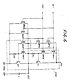
- the Bi-CMOS circuit shown in FIG.6 is a two-input NOR gate.
- a conventional NOR gate 200 is composed of two bipolar transistors Q1 and Q2, two P-channel MOS transistors MP7 and MP8 and two N-channel MOS transistors MN7 and MN8.
- two P-channel MOS transistors MP9 and MP10 and two N-channel MOS transistors MN9 and MN10 are added to the conventional NOR gate 200.
- the MOS transistors MP9 and MP10 are connected in series between the collector and emitter of the bipolar transistor Q1.
- the source of the MOS transistor MP9 is connected to the collector of the bipolar transistor Q1, and the drain thereof is connected to the source of the MOS transistor MP10.
- the drain of the MOS transistor MP10 is connected to the emitter of the bipolar transistor Q1.
- the input signals IN1 and IN2 are applied to the gates of the MOS transistors MP9 and MP10, respectively.
- Each of the MOS transistors MN9 and MN10 are connected between the collector and emitter of the bipolar transistor Q2.
- the input signals IN1 and IN2 are applied to the gates of the MOS transistors MN9 and MN10, respectively.
- the MOS transistors MP7 and MP8 are connected in series between the collector and base of the bipolar transistor Q1. Each of the MOS transistors MN7 and MN8 is connected between the collector and base of the bipolar transistor Q2.
- the input signals IN1 and IN2 are applied to the gates of the MOS transistors MN7 and MN8, respectively.
- the MOS transistors MP7 and MP9 are turned OFF and the MOS transistors MN7 and MN9 are turned ON.
- Current resulting from a charge stored in the load capacitance C passes through the bipolar transistor Q2 so that the output voltage decreases by Vcc - V BE (base-emitter voltage of the bipolar transistor Q2).
- Vcc - V BE base-emitter voltage of the bipolar transistor Q2
- the bipolar transistor Q2 cannot pass current. After that, the current from the load capacitance C starts to pass through the MOS transistor MN9 so that the output voltage becomes equal to the low level rapidly.
Landscapes
- Engineering & Computer Science (AREA)
- Physics & Mathematics (AREA)
- Computer Hardware Design (AREA)
- Computing Systems (AREA)
- General Engineering & Computer Science (AREA)
- Mathematical Physics (AREA)
- Power Engineering (AREA)
- Logic Circuits (AREA)
- Metal-Oxide And Bipolar Metal-Oxide Semiconductor Integrated Circuits (AREA)
Applications Claiming Priority (2)
| Application Number | Priority Date | Filing Date | Title |
|---|---|---|---|
| JP127402/89 | 1989-05-19 | ||
| JP1127402A JPH02305220A (ja) | 1989-05-19 | 1989-05-19 | Bi―cmos回路 |
Publications (2)
| Publication Number | Publication Date |
|---|---|
| EP0398744A2 true EP0398744A2 (de) | 1990-11-22 |
| EP0398744A3 EP0398744A3 (de) | 1991-04-17 |
Family
ID=14959103
Family Applications (1)
| Application Number | Title | Priority Date | Filing Date |
|---|---|---|---|
| EP19900305408 Withdrawn EP0398744A3 (de) | 1989-05-19 | 1990-05-18 | Bi-CMOS-Logikschaltung |
Country Status (4)
| Country | Link |
|---|---|
| US (1) | US5097150A (de) |
| EP (1) | EP0398744A3 (de) |
| JP (1) | JPH02305220A (de) |
| KR (1) | KR900019387A (de) |
Cited By (1)
| Publication number | Priority date | Publication date | Assignee | Title |
|---|---|---|---|---|
| FR2704371A1 (fr) * | 1993-03-17 | 1994-10-28 | Fujitsu Ltd | Circuit Bi-CMOS. |
Families Citing this family (4)
| Publication number | Priority date | Publication date | Assignee | Title |
|---|---|---|---|---|
| JP2607394B2 (ja) * | 1990-11-01 | 1997-05-07 | 株式会社日立製作所 | 非反転バッファ装置および半導体記憶装置 |
| US5287021A (en) * | 1992-05-06 | 1994-02-15 | Motorola, Inc. | Low noise BICMOS circuit |
| US6377088B1 (en) * | 2000-07-21 | 2002-04-23 | Semiconductor Components Industries Llc | Sharp transition push-pull drive circuit with switching signal input circuit |
| JP2004104642A (ja) * | 2002-09-12 | 2004-04-02 | Rohm Co Ltd | トランジスタ出力回路、トランジスタ出力回路を含む半導体装置及び、そのトランジスタ出力回路を備えたスイッチング電源装置 |
Family Cites Families (9)
| Publication number | Priority date | Publication date | Assignee | Title |
|---|---|---|---|---|
| JPH0783252B2 (ja) * | 1982-07-12 | 1995-09-06 | 株式会社日立製作所 | 半導体集積回路装置 |
| JPH0616585B2 (ja) * | 1983-12-16 | 1994-03-02 | 株式会社日立製作所 | バツフア回路 |
| JPS61224519A (ja) * | 1985-03-28 | 1986-10-06 | Toshiba Corp | 論理回路 |
| JPS6235716A (ja) * | 1985-08-09 | 1987-02-16 | Hitachi Ltd | 半導体集積回路装置 |
| JPS6362411A (ja) * | 1986-09-02 | 1988-03-18 | Nec Corp | 半導体回路 |
| JPH07120727B2 (ja) * | 1987-03-27 | 1995-12-20 | 株式会社東芝 | BiMOS論理回路 |
| JPS6468021A (en) * | 1987-09-08 | 1989-03-14 | Mitsubishi Electric Corp | Logic circuit |
| KR920009870B1 (ko) * | 1988-04-21 | 1992-11-02 | 삼성반도체통신 주식회사 | Bi-CMOS 인버터 회로 |
| US4965470A (en) * | 1989-01-30 | 1990-10-23 | Samsung Electronics Co., Ltd. | High integrated Bi-CMOS logic circuit |
-
1989
- 1989-05-19 JP JP1127402A patent/JPH02305220A/ja active Pending
-
1990
- 1990-05-18 US US07/525,058 patent/US5097150A/en not_active Expired - Fee Related
- 1990-05-18 EP EP19900305408 patent/EP0398744A3/de not_active Withdrawn
- 1990-05-19 KR KR1019900007224A patent/KR900019387A/ko not_active Ceased
Cited By (2)
| Publication number | Priority date | Publication date | Assignee | Title |
|---|---|---|---|---|
| FR2704371A1 (fr) * | 1993-03-17 | 1994-10-28 | Fujitsu Ltd | Circuit Bi-CMOS. |
| US5754061A (en) * | 1993-03-17 | 1998-05-19 | Fujitsu Limited | Bi-CMOS circuits with enhanced power supply noise suppression and enhanced speed |
Also Published As
| Publication number | Publication date |
|---|---|
| KR900019387A (ko) | 1990-12-24 |
| EP0398744A3 (de) | 1991-04-17 |
| US5097150A (en) | 1992-03-17 |
| JPH02305220A (ja) | 1990-12-18 |
Similar Documents
| Publication | Publication Date | Title |
|---|---|---|
| US4783604A (en) | Buffer circuit for outputting signals of different polarities | |
| US4985645A (en) | BiCMOS logic circuit having a rapid output voltage falling-down property | |
| US5138195A (en) | Bi-CMOS logic circuit having full voltage swing and rapid turn-off | |
| KR900000487B1 (ko) | 논리 게이트 회로 | |
| JPH0583004B2 (de) | ||
| US4880998A (en) | Bipolar transistor and CMOS transistor logic circuit having improved discharge capabilities | |
| US4948990A (en) | BiCMOS inverter circuit | |
| US5097150A (en) | Bi-cmos logic circuit | |
| US5369318A (en) | Level translator capable of high speed operation | |
| US5331225A (en) | BiCMOS logic circuit with bipolar transistor and MOS transistor formed on the same semiconductor substrate | |
| US5066874A (en) | Signal output circuit having bipolar transistor in output stage and arranged in cmos semiconductor integrated circuit | |
| JPH06232727A (ja) | トライステート可能な駆動回路 | |
| US5247214A (en) | Bi-cmos out buffer circuit for cmos logic | |
| US5182472A (en) | Logic circuit with bipolar CMOS configuration | |
| JPH0795045A (ja) | 半導体集積回路 | |
| US5397937A (en) | Semiconductor integrated circuit | |
| JP3094040B2 (ja) | Cmos論理回路 | |
| JP2538986B2 (ja) | 論理回路 | |
| JP2540928B2 (ja) | 論理回路 | |
| US5495099A (en) | High speed super push-pull logic (SPL) circuit using bipolar technology | |
| JP3207305B2 (ja) | Bimos回路 | |
| JP2641261B2 (ja) | バッファ回路 | |
| JP2934265B2 (ja) | 相補型mos出力回路 | |
| KR930007564B1 (ko) | Fet 풀다운 부하를 가지는 ecl 회로 | |
| JP3233473B2 (ja) | 電圧レベル変換回路 |
Legal Events
| Date | Code | Title | Description |
|---|---|---|---|
| PUAI | Public reference made under article 153(3) epc to a published international application that has entered the european phase |
Free format text: ORIGINAL CODE: 0009012 |
|
| AK | Designated contracting states |
Kind code of ref document: A2 Designated state(s): DE FR GB |
|
| PUAL | Search report despatched |
Free format text: ORIGINAL CODE: 0009013 |
|
| AK | Designated contracting states |
Kind code of ref document: A3 Designated state(s): DE FR GB |
|
| 17P | Request for examination filed |
Effective date: 19910912 |
|
| STAA | Information on the status of an ep patent application or granted ep patent |
Free format text: STATUS: THE APPLICATION HAS BEEN WITHDRAWN |
|
| 18W | Application withdrawn |
Withdrawal date: 19920817 |