EP0399299A2 - Elektrisch leitfähige Polymermaterialien und ihre Anwendungen - Google Patents
Elektrisch leitfähige Polymermaterialien und ihre Anwendungen Download PDFInfo
- Publication number
- EP0399299A2 EP0399299A2 EP90108792A EP90108792A EP0399299A2 EP 0399299 A2 EP0399299 A2 EP 0399299A2 EP 90108792 A EP90108792 A EP 90108792A EP 90108792 A EP90108792 A EP 90108792A EP 0399299 A2 EP0399299 A2 EP 0399299A2
- Authority
- EP
- European Patent Office
- Prior art keywords
- salts
- poly
- group
- electron beam
- polymer
- Prior art date
- Legal status (The legal status is an assumption and is not a legal conclusion. Google has not performed a legal analysis and makes no representation as to the accuracy of the status listed.)
- Withdrawn
Links
Images


Classifications
-
- H—ELECTRICITY
- H05—ELECTRIC TECHNIQUES NOT OTHERWISE PROVIDED FOR
- H05K—PRINTED CIRCUITS; CASINGS OR CONSTRUCTIONAL DETAILS OF ELECTRIC APPARATUS; MANUFACTURE OF ASSEMBLAGES OF ELECTRICAL COMPONENTS
- H05K9/00—Screening of apparatus or components against electric or magnetic fields
- H05K9/0073—Shielding materials
- H05K9/0079—Electrostatic discharge protection, e.g. ESD treated surface for rapid dissipation of charges
-
- C—CHEMISTRY; METALLURGY
- C08—ORGANIC MACROMOLECULAR COMPOUNDS; THEIR PREPARATION OR CHEMICAL WORKING-UP; COMPOSITIONS BASED THEREON
- C08G—MACROMOLECULAR COMPOUNDS OBTAINED OTHERWISE THAN BY REACTIONS ONLY INVOLVING UNSATURATED CARBON-TO-CARBON BONDS
- C08G61/00—Macromolecular compounds obtained by reactions forming a carbon-to-carbon link in the main chain of the macromolecule
- C08G61/12—Macromolecular compounds containing atoms other than carbon in the main chain of the macromolecule
-
- H—ELECTRICITY
- H01—ELECTRIC ELEMENTS
- H01B—CABLES; CONDUCTORS; INSULATORS; SELECTION OF MATERIALS FOR THEIR CONDUCTIVE, INSULATING OR DIELECTRIC PROPERTIES
- H01B1/00—Conductors or conductive bodies characterised by the conductive materials; Selection of materials as conductors
- H01B1/06—Conductors or conductive bodies characterised by the conductive materials; Selection of materials as conductors mainly consisting of other non-metallic substances
- H01B1/12—Conductors or conductive bodies characterised by the conductive materials; Selection of materials as conductors mainly consisting of other non-metallic substances organic substances
- H01B1/124—Intrinsically conductive polymers
- H01B1/127—Intrinsically conductive polymers comprising five-membered aromatic rings in the main chain, e.g. polypyrroles, polythiophenes
-
- H—ELECTRICITY
- H01—ELECTRIC ELEMENTS
- H01B—CABLES; CONDUCTORS; INSULATORS; SELECTION OF MATERIALS FOR THEIR CONDUCTIVE, INSULATING OR DIELECTRIC PROPERTIES
- H01B1/00—Conductors or conductive bodies characterised by the conductive materials; Selection of materials as conductors
- H01B1/06—Conductors or conductive bodies characterised by the conductive materials; Selection of materials as conductors mainly consisting of other non-metallic substances
- H01B1/12—Conductors or conductive bodies characterised by the conductive materials; Selection of materials as conductors mainly consisting of other non-metallic substances organic substances
- H01B1/124—Intrinsically conductive polymers
- H01B1/128—Intrinsically conductive polymers comprising six-membered aromatic rings in the main chain, e.g. polyanilines, polyphenylenes
-
- H—ELECTRICITY
- H01—ELECTRIC ELEMENTS
- H01J—ELECTRIC DISCHARGE TUBES OR DISCHARGE LAMPS
- H01J29/00—Details of cathode-ray tubes or of electron-beam tubes of the types covered by group H01J31/00
- H01J29/86—Vessels; Containers; Vacuum locks
- H01J29/867—Means associated with the outside of the vessel for shielding, e.g. magnetic shields
- H01J29/868—Screens covering the input or output face of the vessel, e.g. transparent anti-static coatings, X-ray absorbing layers
-
- H—ELECTRICITY
- H05—ELECTRIC TECHNIQUES NOT OTHERWISE PROVIDED FOR
- H05K—PRINTED CIRCUITS; CASINGS OR CONSTRUCTIONAL DETAILS OF ELECTRIC APPARATUS; MANUFACTURE OF ASSEMBLAGES OF ELECTRICAL COMPONENTS
- H05K9/00—Screening of apparatus or components against electric or magnetic fields
- H05K9/0073—Shielding materials
- H05K9/0081—Electromagnetic shielding materials, e.g. EMI, RFI shielding
-
- H—ELECTRICITY
- H10—SEMICONDUCTOR DEVICES; ELECTRIC SOLID-STATE DEVICES NOT OTHERWISE PROVIDED FOR
- H10W—GENERIC PACKAGES, INTERCONNECTIONS, CONNECTORS OR OTHER CONSTRUCTIONAL DETAILS OF DEVICES COVERED BY CLASS H10
- H10W42/00—Arrangements for protection of devices
- H10W42/60—Arrangements for protection of devices protecting against electrostatic charges or discharges, e.g. Faraday shields
-
- H—ELECTRICITY
- H10—SEMICONDUCTOR DEVICES; ELECTRIC SOLID-STATE DEVICES NOT OTHERWISE PROVIDED FOR
- H10W—GENERIC PACKAGES, INTERCONNECTIONS, CONNECTORS OR OTHER CONSTRUCTIONAL DETAILS OF DEVICES COVERED BY CLASS H10
- H10W70/00—Package substrates; Interposers; Redistribution layers [RDL]
- H10W70/60—Insulating or insulated package substrates; Interposers; Redistribution layers
- H10W70/67—Insulating or insulated package substrates; Interposers; Redistribution layers characterised by their insulating layers or insulating parts
- H10W70/69—Insulating materials thereof
-
- Y—GENERAL TAGGING OF NEW TECHNOLOGICAL DEVELOPMENTS; GENERAL TAGGING OF CROSS-SECTIONAL TECHNOLOGIES SPANNING OVER SEVERAL SECTIONS OF THE IPC; TECHNICAL SUBJECTS COVERED BY FORMER USPC CROSS-REFERENCE ART COLLECTIONS [XRACs] AND DIGESTS
- Y10—TECHNICAL SUBJECTS COVERED BY FORMER USPC
- Y10T—TECHNICAL SUBJECTS COVERED BY FORMER US CLASSIFICATION
- Y10T428/00—Stock material or miscellaneous articles
- Y10T428/31504—Composite [nonstructural laminate]
- Y10T428/31855—Of addition polymer from unsaturated monomers
Definitions
- This invention relates to electrically conductive polymers, electrically conductive resists, uses thereof and structures fabricated therewith. More particularly, this invention relates to electrically conductive substituted and unsubstituted polyanilines, substituted polyparaphenylenevinylenes, substituted and unsubstituted polythiophenes, polyazines, substituted polyfuranes, substituted polypyrroles, substituted polyselenophene, substituted and unsubstituted poly-p-phenylene sulfides and polyacetylenes formed from soluble precursors and to selectively forming conducting patterns in these materials and the use of these materials as an electrical discharge layer.
- the polyacetylene is impregnated with one of the group of triarylsulfonium and diaryliodonium which are inert to the polyacetylene but which on irradiation with UV light undergo a photochemical reaction leading to the doping of the polyacetylene to make it conductive.
- the impregnated film can be selectively exposed to light through a mask to selectively dope selected regions of the polymer.
- Polyacetylene is not suitable as a resist material since the polyacetylene is not soluble.
- a polymer to be suitable as a resist material it must be capable of having a preselected pattern formed therein, for example on exposure to radiation, with either the exposed or unexposed region being soluble in a solvent while the other of the exposed or unexposed region is insoluble in the solvent.
- an insoluble solid polymer is immersed in a solution containing a dopant material.
- the dopant material and the solvent are absorbed into the surface of the material.
- the solvent in combination with the dopant is exposed to light to render the irradiated part of the polymer electrically conducting. Because of the non-soluble nature of the polymers, the dopants can only be impregnated or absorbed into the surface of the polymer film.
- a pattern in a dielectric layer or an electrically conducting layer can be formed by depositing a resist material thereover.
- a commonly used method of selectively removing the resist material is to selectively expose the resist material to an electron beam.
- the resist material in the exposed region is either made soluble or insoluble upon exposure to the electron beam radiation.
- the solubility of the unexposed region is opposite that of the exposed region. Therefore, the exposed or the unexposed region can be removed.
- the resist material is typically a dielectric.
- the conductive polymer materials of the present invention can also be used as an electrical discharge layer for scanning electron microscopic applications.
- a thin metal layer is coated onto the sample.
- a commonly used metal layer is gold or a mixture of gold with other metals.
- This thin metallic layer acts as an electrical discharge layer to prevent the accumulation of electrical charge on the surface of the sample being examined.
- a metallic material is used as an electrical discharge layer it cannot be easily removed, therefore, the sample being examined must be discarded. This is particularly costly in microelectronic applications where it may be desirable to examine a semiconductor chip or semiconductor chip packaging substrate with an electron microscope where the chip or substrate is functional and useful. Depositing a thin metallic layer onto a substrate would render the chip or substrate not usable.
- Selected regions of films of the materials of the present invention can be made conducting upon the selective exposure to a source of energy.
- These materials can be used to make a patternable conductive resist material and can be used as an electrostatic discharge layer, or as an electromagnetic interference (EMI) layer on the surface of a substrate. Because of the electrostatic properties of these materials they can be used as an electron beam resist which acts as its own discharge layer.
- the materials of the present invention can be readily removed from a surface on which they are deposited, they can be used as a removable electrostatic discharge layer disposed on a dielectric surface under electron beam microscopic examination, for example in a scanning electron microscope (SEM).
- SEM scanning electron microscope
- the dopant reagent and polymer are mixed in a solvent which is thereafter dried to remove the solvents to form a solid solution of the dopant reagent and the polymer.
- the solid solution is then selectively exposed to energy, for example, electromagnetic radiation, heat or an electron beam, which causes the reagent to decompose to dope those regions of the polymer which are exposed to the energy forming a conductive polymer in exposed regions.
- energy for example, electromagnetic radiation, heat or an electron beam
- the polymer is rendered insoluble and in the unexposed regions the polymer is soluble and can thereby be removed to act as a negative photoresist which is selectively electrically conducting.
- a resist material of this kind is particularly useful for electron beam lithographic applications since the resist material can be its own discharge layer.
- a resist material which is on selective exposure to energy, for example electromagnetic radiation, an electron beam or heat, rendered insoluble and at the same time electrically conducting.
- the exposed regions are insoluble and conducting and the unexposed regions are soluble and nonconducting.
- the source of energy generating the pattern is an electron beam
- the pattern which is conducting forms an electron discharge path preventing distortion of the writing beam. If the dielectric layer on which the resist is deposited is thin, the discharge path does not have to be grounded. This avoids the requirement of depositing a metal layer to act as a discharge layer.
- the polymer materials which are made electrically conductive according to the present invention have additional utility in providing an easily processable and low cost EMI (electromagnetic interference) layer which can provide shielding of electrical components from electrical noise.
- EMI electromagnetic interference
- a broad aspect of this invention is a polymeric material which has selected regions which are electrically conductive and insoluble and wherein non-electrically conductive regions are soluble.
- the polymeric material has a partially conjugated ⁇ system which is extended by the addition of dopants to the polymeric material to provide at least enough ⁇ conjugation so that the ⁇ conjugated parts of a molecule of the polymer are substantially in contact with the ⁇ conjugated parts of an adjacent molecule.
- the polymer is selected from substituted polyparaphenylenevinylenes, substituted or unsubstituted polyanilines, substituted polythiophenes, polyazines, substituted or unsubstituted poly-p-phenylene sulfides, substituted polypyrroles, substituted polyselenophene, polyacetylenes formed from soluble precursors, combinations thereof and blends thereof with other polymers.
- a reagent containing a doping species is contained within the polymer matrix.
- the doping species is capable of dissociating upon the application of energy, such as electromagnetic radiation, an electron beam and heat.
- the dissociated species dopes the polymer making it electrically conductive.
- the dopant species is selected from the group of onium salts, iodonium salts, borate salts, tosylate salts, triflate salts and sulfonyloxyimides.
- Another more particular aspect of the present invention is a method of writing and developing a negative image in a polymer wherein the undeveloped portions of the polymer are electrically conducting.
- a solution is formed from a polymer having an extended ⁇ conjugated system with a doping species and a solvent.
- the solution is deposited onto the surface of a substrate, dried to remove the solvent leaving a solid solution of the polymer and the doping species on the surface.
- the solid solution is selectively exposed to energy, for example, electromagnetic radiation, electron beam radiation or heat, to render the selectively exposed regions electrically conductive.
- the unexposed regions are thereafter removed in a solvent leaving a pattern of an electrically conductive polymer.
- a substrate is coated with the electrically conductive polymers according to the present invention, wherein the electrically conductive polymer coating acts as an electrical discharge layer.
- a functional sample can be coated with the polymer, subjected to examination under an electron microscope and thereafter the electrically conductive polymer can be easily removed permitting electron microscopic examination of the functioning part and permitting it to be subsequently used.
- the polymers with the dopant therein according to the present invention are disposed on the surface of a sample for electron beam microscope examination to function as an electrical discharge layer eliminating distortion from accumulated charge on the electron beam irradiated surface.
- One embodiment of the present invention is a polymeric material which can be used as a negative resist material.
- the polymer is disposed onto a substrate and selectively exposed to a source of energy. The energy renders the exposed regions insoluble as compared to the unexposed regions and the exposed regions are rendered electrically conductive.
- These materials are useful as negative resists for microelectronic applications, such as patterning a dielectric or metal layer on the surface of a semiconductor chip or semiconductor chip package substrate.
- the use of these materials as resist material has particular utility in electron beam lithography.
- Resist materials are generally polymers which are dielectrics. If an electron beam is used to write a pattern in a dielectric resist material, electrons can accumulate on the surface of the dielectric resist. These electrons create an electric field which results in distortion of the electron beam which is writing the pattern.
- State of the art electron beam lithography uses electron beams having a cross-sectional size in the order of a micron and less. It does not take much locally accumulated charge to create a distortion in such a small cross-sectional beam. To avoid this problem it is common practice in the art to deposit over a resist material a thin layer of metal. We have discovered a way of avoiding depositing a thin layer of metal onto a resist material to avoid the charging problem.
- the polymers of the present invention can be used as a direct substitute for the metal layer. The polymer is deposited onto the surface of the electron beam resist and exposed to a source of energy to render it conducting. The conducting polymers act as a discharge layer.
- the polymers used to fabricate the resist materials of the present invention contain a partially conjugated ⁇ system.
- a solution is formed of the polymer.
- a doping species dopant precursor
- dopant precursor which on exposure to energy generates a dopant which dopes the polymer to the conducting state.
- the addition of the dopant results in an expansion of the extent of the conjugated ⁇ system in the individual polymer molecule. It is not necessary to extend the conjugated ⁇ system over the full extent of the molecule. It is only necessary to sufficiently extend the ⁇ conjugated system of an individual molecule so that after the solvent is removed the ⁇ conjugated part of an individual molecule is adjacent to a part of the ⁇ conjugated part of an adjacent molecule.
- an electron is essentially delocalized over the entire ⁇ conjugated bonds. These electrons are more loosely bond and are available for electrical conduction.
- an electric field When an electric field is applied, an electron can flow along an individual molecule and hop from one molecule to an adjacent molecule in a region where the ⁇ conjugated parts of the adjacent molecules overlap.
- a ⁇ conjugated system must be soluble when not exposed to the dopant and insoluble when exposed to the dopant.
- Dopants can be a cationic species. The dopant transfers positive charges to the ⁇ conjugated parts of the polymer through protonation, pseudo protonation or oxidation. The polymer now has positive charges on the backbone and then combines with anions to form ion pairs. It is more difficult for a solvent to have enough solvation energy for these ion pairs than for the pristine polymer.
- Nonconducting polymer useful to practice the present invention is a substituted or unsubstituted polyaniline having the following general formula: wherein each R can be H or any organic or inorganic radical; each R can be the same or different; x ⁇ 1; preferably x ⁇ 2 and y has a value from 0 to 1.
- organic radicals are alkyl or aryl radicals.
- inorganic radicals are Si and Ge. This list is exemplary only and not limiting. The most preferred embodiment is the emeraldine base form of the polyaniline wherein y has a value of 0.5.
- the polyaniline base is exposed to a cationic species QA, for example a protic acid wherein Q is hydrogen, the nitrogen atoms of the imine part of the polymer become substituted with the Q cation to form an emeraldine salt as shown in the following equation:
- the emeraldine base form of polyaniline is soluble in various organic solvents and in various aqueous acid solutions.
- organic solvents are dimethylsulfoxide (DMSO), dimethylformamide (DMF) and N-methylpyrrolidinone (NMP). This list is exemplary only and not limiting.
- aqueous acid solutions are 80% acetic acid and 60-88% formic acid. This list is exemplary only and not limiting.
- Substituted polyanilines are soluble in more solvents such as chloroform and methylenechloride.
- a powder of the emeraldine base is mixed in a solvent with a radiation sensitive onium salt.
- the onium salt Upon exposure to radiation the onium salt produces free acid which protonates the emeraldine base to yield an emeraldine salt. Anything that generates a cationic species upon electromagnetic or electron beam radiation can dope the polyaniline polymer.
- onium salts examples include aromatic onium salts of Group IVa elements discussed in U.S Patent 4,175,972, disclosure of which is incorporated herein by reference, and aromatic onium salts of Group Va elements discussed in U.S. Patent 4,069,055, disclosure of which is incorporate herein by reference.
- Radicals included by R are, for example, C (6-13) aromatic hydrocarbon radicals such as phenyl, tolyl, naphthyl, anthryl, and such radicals substituted with up to 1 to 4 monovalent radicals such as C (1-8) alkyl such as methyl and ethyl, substituted alkyl such as -C2H4OCH3, -CH2COOC2H5, -CH2COCH3 , etc.
- R 2 radicals include such structures as:
- MQe (e-f)- of Formula I are, for example, BF - 4 , PF - 6 , SbF - 6 , FeCl - 6 , SbCl - 6 , BiCl - 5 AlF 3- 6 , GaCl - 4 , InF - 4 , TiF - 6 ZrF - 6 , etc., where M is a transition metal such as Sb, Fe, Sn, Bi, Al, Ga, In, Ti, Zr, Sc, V, Cr, Mn, Cs, rare earth elements such as the lanthanides, for example, Ce, Pr, Nd, etc., actinides, such as Th, Pa, U, Np, etc. and metalloids such as B,P and As.
- Group IVa onium salts included by Formula I are, for example:
- Radicals included by R are, for example, C (6-13) aromatic hydrocarbon radicals such as phenyl, tolyl, naphthyl, anthryl and such radicals substituted with up to 1 to 4 monovalent radicals such as C (1-8) alkoxy, C (1-8) alkyl, nitro, chloro, and hydroxy; arylacyl radicals such as phenylacyl; arylalkyl radicals such as pyridyl and furfuryl; R1 radicals include C (1-8) alkyl, C (3-8) cycloalkyl, substituted alkyl such as haloalkyl, for example, choroethyl; alkoxy such as -OCH2C6H5 and -OCH3; alkoxyalkyl such as -CH2COCH3; alkylacyl such as -CH2COOC2H5; ketoalkyl such as -CH2COCH3.
- C (6-13) aromatic hydrocarbon radicals such as pheny
- Radicals included by R2 are, for example: where Q is selected from O, CH2, N, R, and S; Z is selected from -O-, -S- and and R′ is a monovalent radical selected from hydrogen and hydrocarbon.
- Complex anions included by MQe (e-f)- are, for example, BF - 4 , PF - 6 , AsF - 6 , FeCl - 4 , SnCl - 6 , SbCl - 6 , BiCl - 5 , where M is more particularly a transition metal such as Sb, Fe, Sn, Bi, Al, Ga, In, Ti, Zr, Sc, V, Cr, Mn and Co; rare earth elements such as the lanthanides, for example, Ce, Pr and Nd; actinides such as Th, Pa, U and Np; and metalloids such as B, P and As.
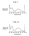
- Fig. 1 shows a uv/visible spectrum of this film. The peaks at 320 nm and 610 nm are characteristic of emeraldine base as seen by comparison with the uv/visible spectrum of emeraldine base alone shown in Fig. 2.
- the film is dried to remove the solvent.
- the uv/visible spectrum of the emeraldine base film contained the onium salt changes. (It is not necessary to filter the radiation, flooding exposure at all wavelengths can be used.)
- the peaks characteristic of the insulating emeraldine base decrease and there is an appearance of an absorption peak around 850 nm which is characteristic of the conducting emeraldine salt.
- the conductivity of the exposed film was measured using a four point probe to be approximately 1.6 ohm ⁇ 1cm ⁇ 1.
- the conductivity can be controlled by controlling the amount of onium salt added to the polyaniline and by the amount of time to which the polymer and onium salt combination is exposed to the radiation.
- the polyaniline becomes insoluble upon exposure.
- an emeraldine base is mixed in solution with an acid which protonates the emeraldine base in solution.
- an onium salt is mixed with the emeraldine base solution, the onium salt does not protonate the polymer to be conductive at this point.
- the solution is disposed onto the surface of a substrate and the solvent is removed by heating to result in a solid solution of the polymer with the onium salt embedded therein.
- the polymer at this point is still not conductive. Only after exposure to electromagnetic radiation, most preferably UV light, or an electron beam does the polymer become conducting.
- Fig. 4 shows a photograph showing an example of the polyaniline onium salt polymer mixture exposed to radiation through a mask to form conducting lines which appear dark in the figure. There is a color change upon exposure. The nonconducting form is blue and the conducting or exposed form is green. The width of these conducting lines are about 2 microns.
- Fig. 5 is a photograph of the pattern of Fig. 4 with the parts of the polymer which have not been exposed to radiation removed by exposure to an organic solvent such as those listed above. Therefore, a negative resist material resulting in conducting lines has been formed.
- Fig. 10 shows a photograph of a polyaniline onium salt combination which has been selectivly exposed to an electron beam to form conducting line having conductivity of 10 ⁇ 2OHM ⁇ 1CM ⁇ 1, width 0.5 ⁇ m and 1.0 ⁇ m spacing.
- the present invention is applicable to a substituted polythiophene.
- Polythiophenes have the general formula: wherein each R2 is H or any organic or inorganic radical; wherein t ⁇ 1 and wherein at least one R2 is not H.
- an onium salt, iodonium salt, a triflate salt, a borate salt, a tosylate salt, a sulfonyloxyimide, or any reagent (referred to herein as a dopant precursor) or oxidizing (a dopant) which dissociates upon exposure to a source of energy to a cationic species is mixed in solution with the polythiophene, deposited on the substrate, dried to remove the solvents and then exposed to either electromagnetic radiation, for example UV radiation, an electron beam, or heat, to convert the polymer to the conductive state.
- Examples 2, 3 and 4 can be repeated using an electron beam of about 200 ⁇ C/cm2 to about 1mC/cm2 at about 25 KeV.
- Polyparaphenylenevinylenes useful to practice the present invention have general formula (V) wherein each R3 is H or any organic or inorganic radical, and wherein s ⁇ 1.
- Each R3 can be the same or different:
- Polyfurans useful to practice the present invention have general formula (VII), wherein Z ⁇ 1 and each R4 is H or any organic radical, and each R4 can be the same or different;
- Polypyrroles which are useful to practice the present invention have general formula (VIII), wherein w ⁇ 1, each R5 is H or any organic or inorganic radical; wherein each R5 can be the same or different:
- Polyselenophenes useful to practice the present invention have general formula (IX), wherein v ⁇ 1, and each R6 is H or any organic or inorganic radical and wherein each R5 can be the same or different:
- R4, R5 and R6 are as defined above, wherein at least two of a, b, c and d are greater than or equal to 1; m ⁇ 1; Q1, Q2, Q3 can be a vinylene group or a direct bond between adjacent constituents:
- Poly-p-phenylene sulfides useful to practice the present invention are represented by the following general formula wherein each R7 is H or any organic or inorganic radical and f ⁇ 1, each R7 can be the same or different:
- Polyacetylene can be prepared from a number of precursors by the use of ring opening metathesis polymerization (ROMP).
- Cyclooctatetraene a high boiling liquid, can be bulk polymerized to polyacetylene. In effect, this provides polyacetylene that can be processed as a viscous liquid.
- Substituted cyclooctatetraenes can be polymerized or co-polymerized to a soluble polymer that can be easily fabricated. Treatment of the polybenzvalene with Lewis acids results in the rearrangement to polyacetylene.
- the polymers of the present invention can be easily spin coated onto a sample and exposed to energy to induce conductivity.
- the conductive polymers of the present invention can be used as top surface electrical discharge layers or as buried electrical discharge layers for electron beam applications.
- the conductive polymers according to the present invention are readily etchable in an oxygen plasma.
- a first resist layer is deposited onto a substrate
- a polymer layer, according to the present invention is deposited thereover and a second resist layer is deposited onto the polymer layer.
- the polymer layer can be made conducting by exposure to electromagnetic radiation, an electron beam or heat.
- the top resist layer When the conducting polymers according to the present invention are used as a buried discharge layer underneath a dielectric resist layer, the top resist layer still charges up. When exposed to an electron beam the degree of charging depends upon the thickness of this top layer. If the resist material is not too thick, charge which accumulates in this top surface layer will leak to the conductive interlayer and flow to ground if the conductive interlayer is grounded. It has been found that the conductive interlayer does not have to be grounded to avoid a distortion of an incident electron beam. It is only necessary that the charge leaks away quick enough so as not to build up any significant potential at the electron beam target point.
- a surface conductivity of approximately 10 ⁇ 6OHM ⁇ 1 is sufficient to avoid distortion of an incident electron beam of approximately 25 KeV with a dose of 15 ⁇ C/cm2. It has been found that this surface resistance will maintain the voltage difference between the target point on the top surface resist and a grounded buried conductive layer at a few volts, preferably less than 1.6V, when an electron beam voltage of approximately 20 KeV is used.
- a volume conductivity of about 10 ⁇ 2OHM ⁇ 1cm ⁇ 1 is needed to achieve a surface conductivity of this value.
- a volume conductivity of about 10 ⁇ 1OHM ⁇ 1cm ⁇ 1 is needed for a 1 micron thick film.
- the polythiophenes of the present invention have been found to be soluble in toluene and xylene and a little less soluble in polar solvents as for example THF (tetrahydrofuran), NMP and anisole. Very good mixing has been achieved between the polythiophenes and MDT in xylenes. Enhanced mixing in other solvents may be achievable by incorporating C-O-C linkages or other polar groups as side chains on the thiophene ring of the polymer.
- Conductivity of the order of 10 OHM ⁇ 1cm ⁇ 1 can be thermally induced in polymers according to the present invention.
- the polymeric conductivity is induced thermally by the use of reagents which on heating generate dopants, for example cations.
- the generated dopants dope the polymer to the metallic regime.
- amine triflate salts When amine triflate salts are heated they unblock to liberate a free acid, triflic acid, and the volatile amine constituent, the temperature at which unblocking occurs depends on the volatility of the amine constituent.
- the general equation of an amine triflate salt is CF3SO3H NR3.
- CF3SO3H a free acid represented by chemical formula CF3SO3H and the volatile amine represented by chemical formula R3N.
- the triflic acid is then capable of protonating the polyaniline as described above.
- Triflic acid is expected to protonate polyparaphenylenevinylenes, polyazines, polyfuranes, polypyrroles, polyselenophenes, poly-p-phenylene sulfides and polyacetylenes.
- NMP solution of the non-conducting polyaniline containing either diethyl ammonium trifluoromethane sulphonate or diisopropyl ammonium trifluoromethane sulfonate was spin-coated onto quartz wafers to yield thin films of approximately 0.2 nm (2,000 angstroms).
- the films were placed on a hot plate at a temperature range from about 80° to 90°C for 3 minutes by which time the films displayed a conductivity in the order of about 1 S/cm.
- triflate salts useful to practice the present invention which are thermally decomposable to a cationic species which can be used to generate dopants useful to practice the present invention includes the triflates, tosylates and borates of the following list: CF3SO3H ⁇ N(C6H5)3 CF3SO3H ⁇ NH3 CF3SO3H ⁇ (CH3)3N CF3SO3H ⁇ C2H5NH2 CF3SO3H ⁇ (C2H5)2NH CF3SO3H ⁇ (C2H5)3N CF3SO3H ⁇ (i-C3H7)2NH CF3SO3H ⁇ (i-C3H7)2N(C2H5) CF3SO3H ⁇ (i-C3H7)2N(C2H4OH) CF3SO3H ⁇ H2N(C2H4OH) CF3SO3H ⁇ HN[(C4H4)O]2 CF3SO3H ⁇ H2NC(CH3)2CH2OH CF
- thermoly decomposing species which generates a cation or oxide species can be used to thermally induce conductivity in the polymers of the present invention.
- the electrically conducting polymers of the present invention have particular usefulness in electron microscopy. Electron microcoscopy is currently used in microelectronics to make observations and dimensional measurements on dielectric masks, for example, quartz/chromium masks used in optical lithography. Charging is caused by the incident electron beam. The current solution to avoid the charging problem is to deposit a thin layer of metal onto the mask. This is, however, a destructive method since complete removal of the metal layer is quite difficult if not impossible. Therefore, scanning electron microscopic observations and measurements are limited to scrapped pieces.
- the conducting polymers of the present invention are readily removable, for example by an oxygen plasma or by undoping in a base, for example, in 0.1M NH4OH and dissolving off in a solvent, for example, NMP, they can be used as a discharge layer in SEM applications. Since the conductive polymers of the present invention are removable, they can be used as a discharge layer on the surface of masks, electronic devices such as semiconductor chips and semiconductor chip packaging substrates which are not scrap pieces.
- any of the conducting polymers according to the present invention can be used as a discharge layer to avoid distortion in electron beam microscopic observations.
- a quartz/chromium mask was observed with a SEM at 10 KV at various resolutions.
- the same mask was coated with an NMP solution of polyaniline which was doped with 1N HCl to result in a conductivity of about 1 S/cm.
- the coated mask was heated to a temperature of about 80°C to drive off the solvent.
- the resulting film thickness was about 0.1 nm (1,000 angstoms).
- the polyaniline coated mask was observed with a SEM.
- Fig. 6 shows a 244 SEM of a bare quartz/chromium mask.
- FIG. 7 shows a low resolution SEM of the same mask with a polyaniline coating.
- Fig. 8 shows a high resolution SEM of a bare mask.
- Fig. 9 shows a 16.4 KV SEM of the mask with a polyaniline coating.
- the masks which are coated with the conductive polyaniline have a substantially higher resolution than the uncoated mask.
- the minimum surface conductivity of the conductive polymer to avoid resolution distortion due to charging of the observed substrate is about 10 ⁇ 6OHM ⁇ 1. Charging was not observed at 10 KV for a conducting polyaniline. Without the conductive coating charging is observed above 2 KV. It is quite surprising that materials having conductivities less than that of metals can act as a discharge layer when they are grounded or not grounded.
- conducting polymers can be made by techniques described herein.
- a solution of a proton donor such as HCl and an emeraldine base form of a polyaniline can be mixed in solution which creates a conductive polymer.
- the solution can be disposed on the sample to be observed under an electron beam.
- the solvent can be driven off by the application of heat to form an electrically conductive polymer layer.
- the polymers fabricated according to the present invention can be used.
- the coated sample can either be exposed to heat or radiation to induce conductivity in the polymer or in the case of the electron beam sensitive cationic species, the electron beam used to make the SEM observation can induce the electrical conductivity in the polymer coating.
- the polymer coating can be removed for example using a plasma etch, such as an oxygen plasma or in the case of a polyaniline doped with HCl the conductive polymer can be removed by a wash with for example a base, such as KOH, followed by an organic solvent, such as NMP.
- a plasma etch such as an oxygen plasma
- the conductive polymer can be removed by a wash with for example a base, such as KOH, followed by an organic solvent, such as NMP.
- the electrically conductive polymer materials of the present invention have additional uses such as an electromagnetic interference (EMI) coating on a dielectric surface.
- EMI electromagnetic interference
- electrical components are frequently contained within dielectric housings such as cabinets, molded plastics and the like.
- the dieletric housing can be coated with the polymeric materials of the present invention.
- This EMI technique is easily implemented in a high volume manufacturing line and has very low cost.
- Continual EMI coatings contain expensive precious metals such as silver embedded in a polymer matrix.
- electrically conductive resist structures and materials have been described which act as their own electrostatic discharge layers.
- the electrical conductivity can be induced in the polymers of the present invention by exposure to sources of energy such as electromagnetic radiation, an electron beam and heat.
- the polymers according to the present invention contain ⁇ conjugated systems which are extended by exposing to dopants such as a cationic species.
- the preferred polymers are selected from the group of substituted and unsubstituted polyanilines, polyparaphenylenevinylenes, polythiophenes, poly-p-phenylene sulfides, polyfuranes, polypyrroles, polyselenophenes, polyacetylenes formed from soluble precursors, combinations thereof and combinations thereof with other materials, blends thereof with other polymers and polymers thereof formed from soluble precursors.
- the polymers can be selectively doped.
- the polymers are useful as buried and surface electrical discharge layers for electron beam lithography applications and for discharge layers for electronmicroscopy applications, for example, scanning electron microscopy.
Landscapes
- Physics & Mathematics (AREA)
- Engineering & Computer Science (AREA)
- Microelectronics & Electronic Packaging (AREA)
- Spectroscopy & Molecular Physics (AREA)
- Chemical & Material Sciences (AREA)
- Medicinal Chemistry (AREA)
- Polymers & Plastics (AREA)
- Organic Chemistry (AREA)
- Chemical Kinetics & Catalysis (AREA)
- Electromagnetism (AREA)
- Health & Medical Sciences (AREA)
- Electron Beam Exposure (AREA)
- Polyoxymethylene Polymers And Polymers With Carbon-To-Carbon Bonds (AREA)
- Polymers With Sulfur, Phosphorus Or Metals In The Main Chain (AREA)
- Macromolecular Compounds Obtained By Forming Nitrogen-Containing Linkages In General (AREA)
- Parts Printed On Printed Circuit Boards (AREA)
- Compositions Of Macromolecular Compounds (AREA)
- Shielding Devices Or Components To Electric Or Magnetic Fields (AREA)
- Organic Insulating Materials (AREA)
- Materials For Photolithography (AREA)
Applications Claiming Priority (2)
| Application Number | Priority Date | Filing Date | Title |
|---|---|---|---|
| US357565 | 1989-05-26 | ||
| US07/357,565 US5198153A (en) | 1989-05-26 | 1989-05-26 | Electrically conductive polymeric |
Publications (2)
| Publication Number | Publication Date |
|---|---|
| EP0399299A2 true EP0399299A2 (de) | 1990-11-28 |
| EP0399299A3 EP0399299A3 (de) | 1991-08-21 |
Family
ID=23406131
Family Applications (1)
| Application Number | Title | Priority Date | Filing Date |
|---|---|---|---|
| EP19900108792 Withdrawn EP0399299A3 (de) | 1989-05-26 | 1990-05-10 | Elektrisch leitfähige Polymermaterialien und ihre Anwendungen |
Country Status (3)
| Country | Link |
|---|---|
| US (1) | US5198153A (de) |
| EP (1) | EP0399299A3 (de) |
| JP (1) | JP2657956B2 (de) |
Cited By (25)
| Publication number | Priority date | Publication date | Assignee | Title |
|---|---|---|---|---|
| WO1992017995A1 (fr) * | 1991-04-02 | 1992-10-15 | Alcatel Cable | Materiau pour ecran semi-conducteur |
| US5266617A (en) * | 1991-04-22 | 1993-11-30 | Allied-Signal Inc. | Lewis base catalyzed phase transfer coating process for polyanilines |
| US5278213A (en) * | 1991-04-22 | 1994-01-11 | Allied Signal Inc. | Method of processing neutral polyanilines in solvent and solvent mixtures |
| EP0615257A3 (de) * | 1993-03-09 | 1994-11-17 | Koninkl Philips Electronics Nv | Verbundstoff mit einer Metallschicht auf einer leitfähigen Polymerschicht und Methode zur Herstellung eines solchen Verbundstoffes. |
| EP0615256A3 (de) * | 1993-03-09 | 1994-11-17 | Koninkl Philips Electronics Nv | Herstellungsverfahren eines Musters von einem elektrisch leitfähigen Polymer auf eine Substratoberfläche und Metallisierungsverfahren solches Musters. |
| US5447824A (en) * | 1993-03-09 | 1995-09-05 | U.S. Philips Corporation | Method of manufacturing a pattern of an electrically conductive polymer on a substrate surface and method of metallizing such a pattern |
| FR2718140A1 (fr) * | 1994-03-31 | 1995-10-06 | France Telecom | Compositions polymériques électriquement conductrices, procédé de fabrication de telles compositions, substrats revêtus avec ces compositions et solutions oxydantes pour leur fabrication. |
| EP0721194A3 (de) * | 1995-01-09 | 1997-03-05 | Ibm | Zersetzte, elektrisch leitfähige Polymere und ihre Verläufer |
| EP0773479A1 (de) * | 1995-11-13 | 1997-05-14 | Motorola, Inc. | Verfahren zur Umwandlung von Polymeren und Strukturierung von einem PPV-Derivat |
| WO1998005043A1 (en) * | 1996-07-25 | 1998-02-05 | International Business Machines Corporation | Vibrational methods of deaggregation of electrically conductive polymers and precursors thereof |
| US5721299A (en) * | 1989-05-26 | 1998-02-24 | International Business Machines Corporation | Electrically conductive and abrasion/scratch resistant polymeric materials, method of fabrication thereof and uses thereof |
| WO1999048122A1 (en) * | 1998-03-13 | 1999-09-23 | The University Of Liverpool | Field emission cathode and field emission display |
| EP1079397A1 (de) * | 1999-08-23 | 2001-02-28 | Agfa-Gevaert N.V. | Verfahren zur Herstellung eines leitenden Musters auf einem Substrat |
| WO2001033649A1 (en) | 1999-11-02 | 2001-05-10 | Koninklijke Philips Electronics N.V. | Method of producing vertical interconnects between thin film microelectronic devices and products comprising such vertical interconnects |
| US6444400B1 (en) | 1999-08-23 | 2002-09-03 | Agfa-Gevaert | Method of making an electroconductive pattern on a support |
| DE10116876A1 (de) * | 2001-04-04 | 2002-10-17 | Infineon Technologies Ag | Selbstjustierte Kontaktdotierung für organische Feldeffekttransistoren |
| WO2003038851A1 (en) * | 2001-11-01 | 2003-05-08 | Massachusetts Institute Of Technology | Organic field emission device |
| DE102004047273A1 (de) * | 2004-09-24 | 2006-04-06 | Infineon Technologies Ag | Elektrisch leitfähiger Resist für die Fotomaskenherstellung |
| KR100736286B1 (ko) * | 2004-06-09 | 2007-07-09 | 후지쯔 가부시끼가이샤 | 다층체, 레지스트 패턴 형성 방법, 미세 가공 패턴을 갖는장치의 제조 방법 및 전자 장치 |
| US7723721B2 (en) | 2001-11-09 | 2010-05-25 | Semiconductor Energy Laboratory Co., Ltd. | Light emitting device having TFT |
| EP1919006A4 (de) * | 2005-07-29 | 2012-10-17 | Consejo Superior Investigacion | Verfahren zum erhalten von mustern in einem organischen leitersubstrat und so erhaltenes organisches material |
| CN103443162A (zh) * | 2011-03-28 | 2013-12-11 | 富士胶片株式会社 | 导电性组合物、使用该组合物的导电性膜及其制备方法 |
| US8609181B2 (en) | 2003-06-16 | 2013-12-17 | Semiconductor Energy Laboratory Co., Ltd. | Light emitting device and method for fabricating light emitting device |
| US8828649B2 (en) | 2005-11-17 | 2014-09-09 | Imperial Innovations Limited | Method of patterning a thin film |
| CN104170021A (zh) * | 2012-05-22 | 2014-11-26 | 太阳控股株式会社 | 导电性组合物及由其形成有导电膜的电路基板 |
Families Citing this family (165)
| Publication number | Priority date | Publication date | Assignee | Title |
|---|---|---|---|---|
| US5917707A (en) | 1993-11-16 | 1999-06-29 | Formfactor, Inc. | Flexible contact structure with an electrically conductive shell |
| JPH0826231B2 (ja) * | 1991-08-16 | 1996-03-13 | インターナショナル・ビジネス・マシーンズ・コーポレイション | 導電性ポリマー材料及びその使用 |
| JPH06125519A (ja) * | 1992-04-28 | 1994-05-06 | Internatl Business Mach Corp <Ibm> | 耐摩耗性・耐スクラッチ性の導電性重合体組成物 |
| JP3112745B2 (ja) * | 1992-06-17 | 2000-11-27 | 富士通株式会社 | パターン形成用導電性組成物及び該組成物を用いたパターン形成方法 |
| US5804354A (en) * | 1992-06-17 | 1998-09-08 | Fujitsu Limited | Composition for forming conductivity imparting agent and pattern forming method |
| EP0579027A1 (de) * | 1992-06-30 | 1994-01-19 | Nitto Denko Corporation | Organische Polymerlösung und Verfahren zur Herstellung von elektrisch leitenden organischen Polymeren |
| JP2751779B2 (ja) * | 1992-08-28 | 1998-05-18 | 日本電気株式会社 | 光分解性高分子化合物およびフォトレジスト組成物 |
| US6399206B1 (en) | 1992-09-30 | 2002-06-04 | The Dow Chemical Company | Electrostatically painted polymers and a process for making same |
| US5340500A (en) * | 1993-02-26 | 1994-08-23 | National Science Council | Conducting pan-layered inorganic composite and preparation of the same |
| US7166241B1 (en) | 1993-03-03 | 2007-01-23 | International Business Machines Corporation | Water-soluble electrically conducting polymers, their synthesis and use |
| US5370825A (en) * | 1993-03-03 | 1994-12-06 | International Business Machines Corporation | Water-soluble electrically conducting polymers, their synthesis and use |
| US5637652A (en) * | 1993-06-04 | 1997-06-10 | Showa Denko Kabushiki Kaisha | Electroconductive polymer and process for producing the same |
| US5820014A (en) | 1993-11-16 | 1998-10-13 | Form Factor, Inc. | Solder preforms |
| US7073254B2 (en) | 1993-11-16 | 2006-07-11 | Formfactor, Inc. | Method for mounting a plurality of spring contact elements |
| US20020053734A1 (en) | 1993-11-16 | 2002-05-09 | Formfactor, Inc. | Probe card assembly and kit, and methods of making same |
| US5571454A (en) * | 1994-03-16 | 1996-11-05 | National Science Council | Soluble and processable doped electrically conductive polymer and polymer blend thereof |
| ES2191057T3 (es) * | 1994-09-06 | 2003-09-01 | Koninkl Philips Electronics Nv | Dispositivo electroluminiscente que comprende una capa de poli-3,4-dioxitiofeno. |
| US5700398A (en) * | 1994-12-14 | 1997-12-23 | International Business Machines Corporation | Composition containing a polymer and conductive filler and use thereof |
| US6087472A (en) * | 1995-01-09 | 2000-07-11 | International Business Machines Corporation | Methods of fabrication of deaggregated electrically conductive polymers and precursors thereof |
| US5804100A (en) * | 1995-01-09 | 1998-09-08 | International Business Machines Corporation | Deaggregated electrically conductive polymers and precursors thereof |
| US6210537B1 (en) * | 1995-06-19 | 2001-04-03 | Lynntech, Inc. | Method of forming electronically conducting polymers on conducting and nonconducting substrates |
| US5716550A (en) * | 1995-08-10 | 1998-02-10 | Eastman Kodak Company | Electrically conductive composition and elements containing solubilized polyaniline complex and solvent mixture |
| US8033838B2 (en) | 1996-02-21 | 2011-10-11 | Formfactor, Inc. | Microelectronic contact structure |
| US5994152A (en) | 1996-02-21 | 1999-11-30 | Formfactor, Inc. | Fabricating interconnects and tips using sacrificial substrates |
| US5767624A (en) * | 1996-06-26 | 1998-06-16 | International Business Machines Corporation | Light emitting device |
| US6099756A (en) * | 1996-07-25 | 2000-08-08 | International Business Machines Corporation | Vibrational methods of deaggregation of electrically conductive polymers and precursors thereof |
| US6132644A (en) * | 1997-05-29 | 2000-10-17 | International Business Machines Corporation | Energy sensitive electrically conductive admixtures |
| US5985516A (en) * | 1997-07-03 | 1999-11-16 | United Microelectronics Corp. | Electron beam imaging method using conducting polyaniline material |
| US6063547A (en) * | 1998-06-11 | 2000-05-16 | Chartered Semiconductor Manufacturing, Ltd. | Physical vapor deposition poly-p-phenylene sulfide film as a bottom anti-reflective coating on polysilicon |
| US6334965B1 (en) | 1999-09-07 | 2002-01-01 | Lynntech, Inc. | Electronically conductive polymers |
| US6936405B2 (en) | 2000-02-22 | 2005-08-30 | Brewer Science Inc. | Organic polymeric antireflective coatings deposited by chemical vapor deposition |
| EP1269258B1 (de) | 2000-02-22 | 2012-01-11 | Brewer Science, Inc. | Organische polymerische antireflexionsbeschichtungen, die durch chemisches aufdampfen abgelagert werden |
| US6406669B1 (en) * | 2001-01-12 | 2002-06-18 | The Regents Of The University Of California | Polyaniline-based optical ammonia detector |
| US7132219B2 (en) * | 2001-02-02 | 2006-11-07 | Brewer Science Inc. | Polymeric antireflective coatings deposited by plasma enhanced chemical vapor deposition |
| DE10133256B4 (de) * | 2001-07-09 | 2007-07-05 | Infineon Technologies Ag | Verfahren zur Herstellung von leitfähigen oder halbleitenden strukturierten Polymeren |
| KR20030010508A (ko) | 2001-07-25 | 2003-02-05 | 메르크 파텐트 게엠베하 | 모노-, 올리고- 및 폴리-4-플루오로티오펜 및 전하 이동물질로서의 이들의 용도 |
| DE60229090D1 (de) | 2001-07-25 | 2008-11-13 | Merck Patent Gmbh | Mono-, Oligo and Poly-3-(1,1-difluoroalkyl)thiophene und ihre Verwendung als Ladungstransportmaterial |
| US6824706B2 (en) | 2001-07-25 | 2004-11-30 | Merck Patent Gesellschaft Mit Beschrank Haftung | Mono-, Oligo- and poly-difluorovinyl-(hetero)arylenes, their synthesis and their use as charge transport materials |
| JP2003046257A (ja) * | 2001-07-30 | 2003-02-14 | Toppan Forms Co Ltd | 導電性高分子を用いた多層回路を備えたプリント配線紙 |
| ATE461237T1 (de) | 2001-08-17 | 2010-04-15 | Merck Patent Gmbh | Konjugierte copolymere aus dithienothiophen und vinylen oder acetylen |
| TWI245795B (en) * | 2001-08-17 | 2005-12-21 | Merck Patent Gmbh | Mono-, oligo- and polyalkylidenefluorenes and their use as charge transport materials |
| ATE473251T1 (de) | 2001-09-29 | 2010-07-15 | Merck Patent Gmbh | Mono-, oligo- und polymere aus benzo(b)thiophen und 2,2'-bisbenzothiophen und ihre verwendung als ladungstransportmaterial |
| US6649327B2 (en) * | 2001-10-25 | 2003-11-18 | The United States Of America As Represented By The Secretary Of The Navy | Method of patterning electrically conductive polymers |
| ATE295872T1 (de) * | 2001-12-10 | 2005-06-15 | Merck Patent Gmbh | Oligomere und polymere enthaltend eine 2,6- azulene gruppe und ihre verwendung als ladungstransport materialien |
| US6863841B2 (en) * | 2001-12-13 | 2005-03-08 | Merck Patent Gmbh | Oxadiazole derivative and its use as charge transport and light emitting material |
| DE60305570T2 (de) * | 2002-04-24 | 2007-05-03 | Merck Patent Gmbh | Reaktive mesogene Benzodithiophene |
| US6852474B2 (en) * | 2002-04-30 | 2005-02-08 | Brewer Science Inc. | Polymeric antireflective coatings deposited by plasma enhanced chemical vapor deposition |
| DE602004016858D1 (de) * | 2003-08-06 | 2008-11-13 | Merck Patent Gmbh | Verfahren zur herstellung von regioregulären polymeren |
| CN100358074C (zh) * | 2004-03-22 | 2007-12-26 | 华南理工大学 | 高分子薄膜场发射阴极材料及其制备方法与装置 |
| US20050255410A1 (en) | 2004-04-29 | 2005-11-17 | Guerrero Douglas J | Anti-reflective coatings using vinyl ether crosslinkers |
| US20070207406A1 (en) * | 2004-04-29 | 2007-09-06 | Guerrero Douglas J | Anti-reflective coatings using vinyl ether crosslinkers |
| US7235344B2 (en) * | 2004-06-30 | 2007-06-26 | Intel Corporation | Energy harvesting molecules and photoresist technology |
| KR100852540B1 (ko) * | 2004-06-30 | 2008-08-18 | 인텔 코포레이션 | 에너지 수확 분자 및 포토레지스트 기술 |
| US8927114B2 (en) * | 2004-11-30 | 2015-01-06 | Semiconductor Energy Laboratory Co., Ltd. | Light emitting element and electronic device using the same |
| KR101182435B1 (ko) * | 2005-02-03 | 2012-09-12 | 삼성디스플레이 주식회사 | 전도성 고분자 패턴막 및 이를 패터닝 하는 방법 그리고 이를 이용하는 유기전계 발광소자 및 그 제조방법 |
| ATE509055T1 (de) * | 2005-08-16 | 2011-05-15 | Merck Patent Gmbh | Verfahren zur polymerisation von thiophen- oder selenophenderivaten |
| EP1754736B1 (de) | 2005-08-16 | 2011-05-11 | Merck Patent GmbH | Verfahren zur Polymerisation von Thiophen- oder Selenophenderivaten |
| US20070077452A1 (en) * | 2005-10-04 | 2007-04-05 | Jie Liu | Organic light emitting devices having latent activated layers and methods of fabricating the same |
| ATE502970T1 (de) | 2005-11-24 | 2011-04-15 | Merck Patent Gmbh | Verfahren zur herstellung von regioregulären polymeren |
| GB2445514B (en) | 2005-11-24 | 2010-01-13 | Merck Patent Gmbh | Regioregular polyselenophenes |
| JP5683104B2 (ja) * | 2006-03-21 | 2015-03-11 | ノヴァレッド・アクチエンゲゼルシャフト | ドープされた有機半導体材料の製造方法及びそのために用いられる配合物 |
| US20100004423A1 (en) | 2006-06-07 | 2010-01-07 | Rieke Metals Inc. | Process for preparation of regioregular poly(3-substituted-thiophene) |
| US7914974B2 (en) | 2006-08-18 | 2011-03-29 | Brewer Science Inc. | Anti-reflective imaging layer for multiple patterning process |
| FR2913430B1 (fr) * | 2007-03-07 | 2011-02-25 | Commissariat Energie Atomique | Materiau composite adhesif a resistivite controlee. |
| US7831225B2 (en) * | 2007-07-26 | 2010-11-09 | The United States Of America As Represented By The Administrator Of The National Aeronautics And Space Administration | Radio frequency power load and associated method |
| US20100234478A1 (en) * | 2007-10-29 | 2010-09-16 | Base Se | Process for preparation of conducting polymers |
| JP2011508954A (ja) * | 2008-01-04 | 2011-03-17 | オルメコン・ゲーエムベーハー | ポリチオフェンおよびその誘導体に基づく高い導電率を示す塗膜の製造方法 |
| US8133659B2 (en) * | 2008-01-29 | 2012-03-13 | Brewer Science Inc. | On-track process for patterning hardmask by multiple dark field exposures |
| KR101683026B1 (ko) * | 2008-04-11 | 2016-12-07 | 닛산 가가쿠 고교 가부시키 가이샤 | 도핑된 공액 중합체, 소자, 및 소자의 제조 방법 |
| WO2010000669A1 (en) * | 2008-07-02 | 2010-01-07 | Basf Se | Poly(5,5'bis(thiophen-2-yl)-benzo[2,1-b;3,4-b']dithiophene) and its use as high performance solution processable semiconducting polymer |
| TWI471328B (zh) * | 2008-07-02 | 2015-02-01 | 巴地斯顏料化工廠 | 以二噻吩并〔2,3-d:2’,3’-d’〕苯并〔1,2-b:4,5-b’〕二噻吩為主之高效能溶液可加工之半導體 |
| WO2010000755A1 (en) * | 2008-07-02 | 2010-01-07 | Basf Se | High performance solution processable semiconducting polymers based on alternat-ing donor acceptor copolymers |
| EP2315793B1 (de) | 2008-08-18 | 2013-08-21 | Merck Patent GmbH | Indacenodithiophen- und indacenodiselenophenpolymere und ihre verwendung als organische halbleiter |
| CN102159618B (zh) | 2008-09-19 | 2014-11-12 | 默克专利股份有限公司 | 衍生自苯并双(噻咯并噻吩)的聚合物和它们作为有机半导体的应用 |
| WO2010031479A1 (en) | 2008-09-19 | 2010-03-25 | Merck Patent Gmbh | Polymers derived from bis(thienocyclopenta)benzothiadiazole and their use as organic semiconductors |
| US9640396B2 (en) * | 2009-01-07 | 2017-05-02 | Brewer Science Inc. | Spin-on spacer materials for double- and triple-patterning lithography |
| KR20120055669A (ko) | 2009-08-12 | 2012-05-31 | 메르크 파텐트 게엠베하 | 페난트로[1,10,9,8?c,d,e,f,g]카르바졸 중합체 및 유기 반도체로서의 이의 용도 |
| US8389670B2 (en) | 2009-12-02 | 2013-03-05 | Basf Se | Dithienobenzo-thieno[3,2-B]thiophene-copolymer and its use as high performance solution processable semiconducting polymer |
| JP5801322B2 (ja) | 2010-02-15 | 2015-10-28 | メルク パテント ゲゼルシャフト ミット ベシュレンクテル ハフツングMerck Patent Gesellschaft mit beschraenkter Haftung | 半導体ポリマー |
| US9212260B2 (en) | 2010-03-24 | 2015-12-15 | Merck Patent Gmbh | Polymers of 8,9-dihydrobenzo[def]carbazole and their use as organic semiconductors |
| CN102834945A (zh) | 2010-03-31 | 2012-12-19 | 巴斯夫欧洲公司 | 稠合的二噻吩共聚物 |
| JP5847800B2 (ja) | 2010-04-19 | 2016-01-27 | メルク パテント ゲゼルシャフト ミット ベシュレンクテル ハフツングMerck Patent Gesellschaft mit beschraenkter Haftung | ベンゾジチオフェンのポリマーおよび有機半導体としてのそれらの使用 |
| US8877546B2 (en) * | 2010-05-28 | 2014-11-04 | Corning Incorporated | Enhanced semiconductor devices employing photoactive organic materials and methods of manufacturing same |
| KR20130135830A (ko) | 2010-07-08 | 2013-12-11 | 메르크 파텐트 게엠베하 | 반전도성 중합체 |
| GB2494607B (en) | 2010-07-09 | 2018-05-02 | Merck Patent Gmbh | Semiconducting polymers |
| EP2603499A2 (de) | 2010-08-13 | 2013-06-19 | Merck Patent GmbH | Anthra[2,3-b:7,6-b']dithiophenderivate und ihre verwendung als organische halbleiter |
| GB2496565B (en) | 2010-09-04 | 2017-05-17 | Merck Patent Gmbh | Conjugated polymers based on BTZ dicarboxylic acid bis-ester monomers and analogues thereof |
| EP2614068A1 (de) | 2010-09-10 | 2013-07-17 | Merck Patent GmbH | Anthra[2,3-b:7,6b']dithiophenderivate und und ihre verwendung als organische halbleiter |
| RU2013122682A (ru) | 2010-10-20 | 2014-11-27 | Мерк Патент Гмбх | Сопряжённые полимеры |
| RU2013130877A (ru) | 2010-12-06 | 2015-01-20 | Мерк Патент Гмбх | Нелинейные аценовые производные и их применение в качестве органических полупроводников |
| WO2012079675A2 (en) | 2010-12-17 | 2012-06-21 | Merck Patent Gmbh | Conjugated polymers |
| US9373801B2 (en) | 2011-01-28 | 2016-06-21 | Merck Patent Gmbh | Flavanthrene derivatives and their use as organic semiconductors |
| CN103415526A (zh) | 2011-03-11 | 2013-11-27 | 默克专利股份有限公司 | 二萘并[2,3-a:2’,3’-h]吩嗪类和它们作为有机半导体的用途 |
| KR20140023923A (ko) | 2011-03-11 | 2014-02-27 | 메르크 파텐트 게엠베하 | 공액 중합체 |
| JP2014516468A (ja) | 2011-03-25 | 2014-07-10 | メルク パテント ゲゼルシャフト ミット ベシュレンクテル ハフツング | ピロロ[3,2−b]ピロール−2,5−ジオンおよび有機半導体としてのそれらの使用 |
| EP2699617A1 (de) | 2011-04-18 | 2014-02-26 | Merck Patent GmbH | Konjugierte polymere |
| US20140061538A1 (en) | 2011-05-16 | 2014-03-06 | Merck Patent Gmbh | Conjugated polymers |
| KR20140063579A (ko) | 2011-06-28 | 2014-05-27 | 메르크 파텐트 게엠베하 | 유기 반도체로서의 인다세노 유도체 |
| KR20140068009A (ko) | 2011-07-08 | 2014-06-05 | 메르크 파텐트 게엠베하 | 공액 중합체 |
| EP2734528B1 (de) | 2011-07-19 | 2017-03-29 | Merck Patent GmbH | Organische halbleiter |
| WO2013010615A1 (en) | 2011-07-21 | 2013-01-24 | Merck Patent Gmbh | Conjugated polymers |
| JP2014529343A (ja) | 2011-07-27 | 2014-11-06 | メルク パテント ゲゼルシャフト ミット ベシュレンクテル ハフツングMerck Patent Gesellschaft mit beschraenkter Haftung | 小分子および有機半導体としてのそれらの使用 |
| CN103842402B (zh) | 2011-09-28 | 2018-12-11 | 默克专利股份有限公司 | 共轭聚合物 |
| JP2015501303A (ja) | 2011-10-20 | 2015-01-15 | メルク パテント ゲゼルシャフト ミット ベシュレンクテル ハフツングMerck Patent Gesellschaft mit beschraenkter Haftung | 有機半導体 |
| US8658805B2 (en) | 2011-11-07 | 2014-02-25 | Samsung Electronics Co., Ltd. | Fused polyheteroaromatic compound, organic thin film including the compound, and electronic device including the organic thin film |
| US8902015B1 (en) | 2011-11-18 | 2014-12-02 | The United States Of America As Represented By The Administrator Of The National Aeronautics And Space Administration | Radio frequency power load and associated method |
| KR20140135747A (ko) | 2012-02-15 | 2014-11-26 | 메르크 파텐트 게엠베하 | 공액 중합체 |
| EP2814863B1 (de) | 2012-02-15 | 2017-11-15 | Merck Patent GmbH | Konjugierte polymere |
| KR20140135749A (ko) | 2012-02-16 | 2014-11-26 | 메르크 파텐트 게엠베하 | 유기 반도체성 중합체 |
| TWI635111B (zh) | 2012-03-16 | 2018-09-11 | Merck Patent Gmbh | 共軛聚合物 |
| CN104245787B (zh) | 2012-04-25 | 2017-02-22 | 默克专利股份有限公司 | 共轭聚合物 |
| CN104245786B (zh) | 2012-04-25 | 2017-01-25 | 默克专利股份有限公司 | 共轭聚合物 |
| EP2856531A1 (de) | 2012-06-04 | 2015-04-08 | Merck Patent GmbH | Organische halbleiter |
| EP2671880B1 (de) | 2012-06-05 | 2015-09-16 | Samsung Electronics Co., Ltd | Kondensierte polycyclische heteroaromatische Verbindung, organische Dünnschicht mit der Verbindung und elektronische Vorrichtung mit einer organischen Dünnschicht |
| KR20150024386A (ko) | 2012-06-05 | 2015-03-06 | 메르크 파텐트 게엠베하 | 소분자 및 유기 반도체로서의 이의 용도 |
| CN104395372B (zh) | 2012-07-02 | 2017-04-05 | 默克专利股份有限公司 | 共轭聚合物 |
| GB2520464A (en) | 2012-08-24 | 2015-05-20 | Merck Patent Gmbh | Conjugated polymers |
| WO2014086457A1 (en) | 2012-12-07 | 2014-06-12 | Merck Patent Gmbh | Polymer comprising a naphthalene group and its use in organic electronic devices |
| CN104854175A (zh) | 2012-12-18 | 2015-08-19 | 默克专利股份有限公司 | 包含噻二唑基的聚合物、这种聚合物的制备和它在有机电子器件中的用途 |
| JP6438946B2 (ja) | 2013-06-21 | 2018-12-19 | メルク パテント ゲーエムベーハー | 共役ポリマー |
| CN105531267B (zh) | 2013-09-11 | 2018-11-30 | 默克专利有限公司 | 环己二烯富勒烯衍生物 |
| CN104513262A (zh) | 2013-09-30 | 2015-04-15 | 默克专利股份有限公司 | 氮杂硼杂苯衍生物,它们的合成及其在有机电子器件中的用途 |
| KR20160076528A (ko) | 2013-10-22 | 2016-06-30 | 메르크 파텐트 게엠베하 | 공액 중합체 |
| US20160272753A1 (en) | 2013-11-06 | 2016-09-22 | Merck Patent Gmbh | Conjugated polymers |
| JP6591417B2 (ja) | 2013-11-28 | 2019-10-16 | メルク パテント ゲゼルシャフト ミット ベシュレンクテル ハフツングMerck Patent Gesellschaft mit beschraenkter Haftung | チオフェン単位を含む新規の多環式ポリマー、かかるポリマーの製造方法および使用 |
| CN106103436B (zh) | 2014-03-17 | 2019-07-09 | 默克专利股份有限公司 | 有机半导体化合物 |
| JP6546602B2 (ja) | 2014-03-31 | 2019-07-17 | メルク パテント ゲゼルシャフト ミット ベシュレンクテル ハフツングMerck Patent Gesellschaft mit beschraenkter Haftung | 縮合ビスアリールフラーレン誘導体 |
| US10636974B2 (en) | 2014-04-24 | 2020-04-28 | The Trustees Of Columbia University In The City Of New York | Molecular compositions, materials, and methods for efficient multiple exciton generation |
| CN106458808B (zh) | 2014-06-17 | 2021-04-20 | 天光材料科技股份有限公司 | 富勒烯衍生物 |
| KR102502528B1 (ko) | 2014-07-29 | 2023-02-21 | 메르크 파텐트 게엠베하 | 테트라-헤테로아릴 인다세노디티오펜계 폴리시클릭 중합체 및 이들의 용도 |
| US10720259B2 (en) * | 2014-09-02 | 2020-07-21 | Tokyo University Of Science Foundation | Electroconductive film and method for manufacturing electroconductive pattern |
| US9666327B2 (en) * | 2014-09-11 | 2017-05-30 | Shin-Etsu Chemical Co., Ltd. | Conductive polymer material and substrate |
| US9663656B2 (en) * | 2014-09-12 | 2017-05-30 | Shin-Etsu Chemical Co., Ltd. | Conductive polymer material and substrate |
| EP3070756B9 (de) | 2015-03-18 | 2021-11-03 | Raynergy Tek Inc. | Halbleitermischungen mit nanopartikeln |
| KR102541669B1 (ko) | 2015-05-12 | 2023-06-08 | 메르크 파텐트 게엠베하 | 티아디아졸로피리딘 중합체, 이의 합성 및 이의 용도 |
| EP3332432B1 (de) | 2015-08-06 | 2019-08-21 | Merck Patent GmbH | Organische elektronische vorrichtung und deren herstellung |
| EP3151297A1 (de) | 2015-09-30 | 2017-04-05 | InnovationLab GmbH | Konjugierte polymere mit thermisch abspaltbaren oxalatseitengruppen |
| US20190088891A1 (en) | 2016-03-15 | 2019-03-21 | Merck Patent Gmbh | Organic semiconductors |
| US11130837B2 (en) | 2016-03-15 | 2021-09-28 | Raynergy Tek Incorporation | Organic semiconductors |
| EP3481832A1 (de) | 2016-07-08 | 2019-05-15 | Merck Patent GmbH | Kondensierte dithienothiophenderivate und deren verwendung als organische halbleiter |
| CN109415380A (zh) | 2016-07-08 | 2019-03-01 | 默克专利有限公司 | 有机半导体化合物 |
| US11098050B2 (en) | 2016-08-11 | 2021-08-24 | Merck Patent Gmbh | Organic semiconducting compounds comprising a tetraazapyrene core |
| US20190214581A1 (en) | 2016-08-22 | 2019-07-11 | Merck Patent Gmbh | Organic semiconducting compounds |
| US20190189925A1 (en) | 2016-08-29 | 2019-06-20 | Merck Patent Gmbh | Organic semiconductors |
| US10991893B2 (en) | 2016-10-05 | 2021-04-27 | Raynergy Tek Incorporation | Organic semiconducting compounds |
| EP3523836B1 (de) | 2016-10-05 | 2024-09-11 | Raynergy Tek Inc. | Organische halbleitermaterialien |
| EP3306690B1 (de) | 2016-10-05 | 2022-09-07 | Raynergy Tek Inc. | Organische halbleiterverbindungen |
| WO2018078080A1 (en) | 2016-10-31 | 2018-05-03 | Merck Patent Gmbh | Organic semiconducting compounds |
| EP3333170B1 (de) | 2016-12-06 | 2020-04-29 | Merck Patent GmbH | Asymmetrische polyzyklische verbindungen zur verwendung in organischen halbleitern |
| JP7116075B2 (ja) | 2017-03-09 | 2022-08-09 | レイナジー テック インコーポレイション | 有機半導体化合物 |
| WO2019030382A1 (en) | 2017-08-11 | 2019-02-14 | Merck Patent Gmbh | ORGANIC SEMICONDUCTOR POLYMER |
| WO2019052935A1 (en) | 2017-09-13 | 2019-03-21 | Merck Patent Gmbh | ORGANIC SEMICONDUCTOR COMPOUNDS |
| CN111315796B (zh) | 2017-11-02 | 2023-11-24 | 天光材料科技股份有限公司 | 有机半导体化合物 |
| US12101992B2 (en) | 2017-11-10 | 2024-09-24 | Raynergy Tek Incorporation | Organic semiconducting compounds |
| WO2019154973A1 (en) | 2018-02-12 | 2019-08-15 | Merck Patent Gmbh | Organic semiconducting compounds |
| US12532662B2 (en) | 2018-03-28 | 2026-01-20 | Raynergy Tek Incorporation | Organic semiconducting compounds |
| WO2019185578A1 (en) | 2018-03-28 | 2019-10-03 | Merck Patent Gmbh | Organic semiconducting compounds |
| WO2019206926A1 (en) | 2018-04-27 | 2019-10-31 | Merck Patent Gmbh | Organic semiconducting polymers |
| US12193317B2 (en) | 2018-07-13 | 2025-01-07 | Flexenable Technology Limited | Organic semiconducting compounds |
| CN112955456A (zh) | 2018-09-06 | 2021-06-11 | 天光材料科技股份有限公司 | 有机半导体化合物 |
| WO2020161052A1 (en) | 2019-02-06 | 2020-08-13 | Merck Patent Gmbh | Organic semiconducting polymers |
| WO2020178298A1 (en) | 2019-03-07 | 2020-09-10 | Raynergy Tek Inc. | Organic semiconducting composition |
| CN113631627A (zh) | 2019-03-19 | 2021-11-09 | 天光材料科技股份有限公司 | 有机半导体 |
| US11930694B2 (en) | 2020-06-08 | 2024-03-12 | University Of Waterloo | Polymer semiconductors containing acrylyl or acrylyl-like side chain and their devices |
| CN113355107A (zh) * | 2021-07-05 | 2021-09-07 | 合肥中聚合臣电子材料有限公司 | 一种液晶取向剂 |
Family Cites Families (20)
| Publication number | Priority date | Publication date | Assignee | Title |
|---|---|---|---|---|
| US3865597A (en) * | 1973-03-26 | 1975-02-11 | Western Electric Co | Additives to negative photoresists which increase the sensitivity thereof |
| US4222903A (en) * | 1978-05-04 | 1980-09-16 | University Patents, Inc. | P-Type electrically conducting doped polyacetylene film and method of preparing same |
| US4440669A (en) * | 1979-03-20 | 1984-04-03 | Allied Corporation | Electrically conducting compositions of doped polyphenylenes and shaped articles comprising the same |
| DE3049551A1 (de) * | 1980-12-31 | 1982-07-29 | Basf Ag, 6700 Ludwigshafen | Elektrisch leitfaehige poly(pyrrol)-derivate |
| DE3105948A1 (de) * | 1981-02-18 | 1982-08-19 | Basf Ag, 6700 Ludwigshafen | Verfahren zur herstellung von stabilen elekrisch leitfaehigen polymeren systemen und deren verwendung in der elektrotechnik und zur antistatischen ausruestung von kunststoffen |
| DE3118630A1 (de) * | 1981-05-11 | 1982-11-25 | Basf Ag, 6700 Ludwigshafen | Verfahren zur herstellung von elektrisch leitfaehigen polymeren und deren verwendung in der elektrotechnik und zur antistatischen ausruestung von kunststoffen |
| US4491605A (en) * | 1982-06-23 | 1985-01-01 | Massachusetts Institute Of Technology | Conductive polymers formed by ion implantation |
| DE3223544A1 (de) * | 1982-06-24 | 1983-12-29 | Basf Ag, 6700 Ludwigshafen | Copolymere von pyrrolen, verfahren zu ihrer herstellung sowie ihre verwendung |
| US4511494A (en) * | 1982-09-30 | 1985-04-16 | Allied Corporation | Solution of a chalcogen-containing polymer and process of forming conducting polymer articles therefrom |
| US4616067A (en) * | 1983-11-23 | 1986-10-07 | Gte Laboratories Incorporated | Electrically conductive polymer blends of an acetylene polymer and a triblock thermoplastic elastomer |
| US4647403A (en) * | 1984-07-13 | 1987-03-03 | Gte Laboratories Incorporated | Ion implanted polydiacetylenes |
| DE3531600A1 (de) * | 1985-09-04 | 1987-03-05 | Wacker Chemie Gmbh | Polymere mit konjugierten doppelbindungen |
| US4680236A (en) * | 1986-02-18 | 1987-07-14 | The Bf Goodrich Company | Electrodeless heterogeneous polypyrrole composite |
| US4692225A (en) * | 1986-07-08 | 1987-09-08 | Rockwell International Corporation | Method of stabilizing conductive polymers |
| EP0261286B1 (de) * | 1986-09-24 | 1991-08-28 | Katsumi Yoshino | Verfahren und Elemente zur Strahlungsdetektion |
| US5006278A (en) * | 1987-01-12 | 1991-04-09 | Allied-Signal | Solution processible forms of electrically conductive polyaniline and the method of manufacture of electroconductive articles therefrom |
| US4857426A (en) * | 1987-08-01 | 1989-08-15 | The British Petroleum Company P.L.C. | Photo polymers and uses thereof |
| US5028354A (en) * | 1987-10-05 | 1991-07-02 | Regents Of The University Of California | Conductive articles of intractable polymers method for making |
| US5021586A (en) * | 1989-03-31 | 1991-06-04 | Miles, Inc. | Dithiophenylpyrrole derivative monomers for preparing semi-conducting polymers |
| US5021193A (en) * | 1989-06-30 | 1991-06-04 | United States Department Of Energy | Nonaqueous polypyrrole colloids |
-
1989
- 1989-05-26 US US07/357,565 patent/US5198153A/en not_active Expired - Lifetime
-
1990
- 1990-04-26 JP JP2108996A patent/JP2657956B2/ja not_active Expired - Lifetime
- 1990-05-10 EP EP19900108792 patent/EP0399299A3/de not_active Withdrawn
Cited By (51)
| Publication number | Priority date | Publication date | Assignee | Title |
|---|---|---|---|---|
| US5721299A (en) * | 1989-05-26 | 1998-02-24 | International Business Machines Corporation | Electrically conductive and abrasion/scratch resistant polymeric materials, method of fabrication thereof and uses thereof |
| EP0507676A3 (de) * | 1991-04-02 | 1992-11-25 | Alcatel Cable | Material für Halbleiter-Abschirmung |
| US5416155A (en) * | 1991-04-02 | 1995-05-16 | Alcatel Cable | Material for semiconductive screening |
| WO1992017995A1 (fr) * | 1991-04-02 | 1992-10-15 | Alcatel Cable | Materiau pour ecran semi-conducteur |
| US5266617A (en) * | 1991-04-22 | 1993-11-30 | Allied-Signal Inc. | Lewis base catalyzed phase transfer coating process for polyanilines |
| US5278213A (en) * | 1991-04-22 | 1994-01-11 | Allied Signal Inc. | Method of processing neutral polyanilines in solvent and solvent mixtures |
| EP0615257A3 (de) * | 1993-03-09 | 1994-11-17 | Koninkl Philips Electronics Nv | Verbundstoff mit einer Metallschicht auf einer leitfähigen Polymerschicht und Methode zur Herstellung eines solchen Verbundstoffes. |
| EP0615256A3 (de) * | 1993-03-09 | 1994-11-17 | Koninkl Philips Electronics Nv | Herstellungsverfahren eines Musters von einem elektrisch leitfähigen Polymer auf eine Substratoberfläche und Metallisierungsverfahren solches Musters. |
| US5447824A (en) * | 1993-03-09 | 1995-09-05 | U.S. Philips Corporation | Method of manufacturing a pattern of an electrically conductive polymer on a substrate surface and method of metallizing such a pattern |
| US5885711A (en) * | 1994-03-31 | 1999-03-23 | France Telecom | Electrically conductive polymer compositions, production process and coated substrates |
| WO1995027289A1 (fr) * | 1994-03-31 | 1995-10-12 | France Telecom | Compositions polymeriques electriquement conductrices, procede de fabrication et substrats revetus |
| FR2718140A1 (fr) * | 1994-03-31 | 1995-10-06 | France Telecom | Compositions polymériques électriquement conductrices, procédé de fabrication de telles compositions, substrats revêtus avec ces compositions et solutions oxydantes pour leur fabrication. |
| EP0721194A3 (de) * | 1995-01-09 | 1997-03-05 | Ibm | Zersetzte, elektrisch leitfähige Polymere und ihre Verläufer |
| EP0773479A1 (de) * | 1995-11-13 | 1997-05-14 | Motorola, Inc. | Verfahren zur Umwandlung von Polymeren und Strukturierung von einem PPV-Derivat |
| WO1998005043A1 (en) * | 1996-07-25 | 1998-02-05 | International Business Machines Corporation | Vibrational methods of deaggregation of electrically conductive polymers and precursors thereof |
| WO1998005044A1 (en) * | 1996-07-25 | 1998-02-05 | International Business Machines Corporation | Oxidative/reductive methods of deaggregation of electrically conductive polymers and precursors thereof and methods of fabricating articles therewith |
| WO1999048122A1 (en) * | 1998-03-13 | 1999-09-23 | The University Of Liverpool | Field emission cathode and field emission display |
| US6853127B1 (en) | 1998-03-13 | 2005-02-08 | The University Of Liverpool | Field emission cathode and field emission display |
| EP1079397A1 (de) * | 1999-08-23 | 2001-02-28 | Agfa-Gevaert N.V. | Verfahren zur Herstellung eines leitenden Musters auf einem Substrat |
| US6444400B1 (en) | 1999-08-23 | 2002-09-03 | Agfa-Gevaert | Method of making an electroconductive pattern on a support |
| US6635406B1 (en) | 1999-11-02 | 2003-10-21 | Koninklijke Philips Electronics N.V. | Method of producing vertical interconnects between thin film microelectronic devices and products comprising such vertical interconnects |
| WO2001033649A1 (en) | 1999-11-02 | 2001-05-10 | Koninklijke Philips Electronics N.V. | Method of producing vertical interconnects between thin film microelectronic devices and products comprising such vertical interconnects |
| GB2379085A (en) * | 2001-04-04 | 2003-02-26 | Infineon Technologies Ag | Method for doping electrically conductive organic compounds |
| DE10116876A1 (de) * | 2001-04-04 | 2002-10-17 | Infineon Technologies Ag | Selbstjustierte Kontaktdotierung für organische Feldeffekttransistoren |
| DE10116876B4 (de) * | 2001-04-04 | 2004-09-23 | Infineon Technologies Ag | Verfahren zur Dotierung elektrisch leitfähiger organischer Verbindungen, organischer Feldeffekttransistor sowie Verfahren zu dessen Herstellung |
| GB2379085B (en) * | 2001-04-04 | 2005-10-26 | Infineon Technologies Ag | Doping electrically conductive organic compounds |
| WO2003038851A1 (en) * | 2001-11-01 | 2003-05-08 | Massachusetts Institute Of Technology | Organic field emission device |
| US6870312B2 (en) | 2001-11-01 | 2005-03-22 | Massachusetts Institute Of Technology | Organic field emission device |
| US7723721B2 (en) | 2001-11-09 | 2010-05-25 | Semiconductor Energy Laboratory Co., Ltd. | Light emitting device having TFT |
| US9054199B2 (en) | 2001-11-09 | 2015-06-09 | Semiconductor Energy Laboratory Co., Ltd. | Light emitting device |
| US8154015B2 (en) | 2001-11-09 | 2012-04-10 | Semiconductor Energy Laboratory Co., Ltd. | Light-emitting device including thin film transistor |
| US11063102B2 (en) | 2001-11-09 | 2021-07-13 | Semiconductor Energy Laboratory Co., Ltd. | Light emitting device |
| US8324618B2 (en) | 2001-11-09 | 2012-12-04 | Semiconductor Energy Laboratory Co., Ltd. | Light emitting device |
| US10680049B2 (en) | 2001-11-09 | 2020-06-09 | Semiconductor Energy Laboratory Co., Ltd. | Light emitting device |
| US8648338B2 (en) | 2001-11-09 | 2014-02-11 | Semiconductor Energy Laboratory Co., Ltd. | Light emitting device comprising an organic compound layer |
| US10461140B2 (en) | 2001-11-09 | 2019-10-29 | Semiconductor Energy Laboratory Co., Ltd. | Light emitting device |
| US9905624B2 (en) | 2001-11-09 | 2018-02-27 | Semiconductor Energy Laboratory Co., Ltd. | Light emitting device |
| US8609181B2 (en) | 2003-06-16 | 2013-12-17 | Semiconductor Energy Laboratory Co., Ltd. | Light emitting device and method for fabricating light emitting device |
| KR100736286B1 (ko) * | 2004-06-09 | 2007-07-09 | 후지쯔 가부시끼가이샤 | 다층체, 레지스트 패턴 형성 방법, 미세 가공 패턴을 갖는장치의 제조 방법 및 전자 장치 |
| EP1612603A3 (de) * | 2004-06-09 | 2007-08-01 | Fujitsu Limited | Verfahren zur Herstellung von Resistmustern und durch dieses Verfahren erhaltene, elektronische Vorrichtung |
| US8313892B2 (en) | 2004-06-09 | 2012-11-20 | Fujitsu Limited | Multi-layer body, method for forming resist pattern, method for manufacturing device having pattern by fine processing and electronic device |
| DE102004047273A1 (de) * | 2004-09-24 | 2006-04-06 | Infineon Technologies Ag | Elektrisch leitfähiger Resist für die Fotomaskenherstellung |
| EP1919006A4 (de) * | 2005-07-29 | 2012-10-17 | Consejo Superior Investigacion | Verfahren zum erhalten von mustern in einem organischen leitersubstrat und so erhaltenes organisches material |
| US8828649B2 (en) | 2005-11-17 | 2014-09-09 | Imperial Innovations Limited | Method of patterning a thin film |
| EP2692762A4 (de) * | 2011-03-28 | 2015-08-19 | Fujifilm Corp | Elektrisch leitfähige zusammensetzung, elektrisch leitfähiger film mit dieser zusammensetzung und herstellungsverfahren dafür |
| US9445501B2 (en) | 2011-03-28 | 2016-09-13 | Fujifilm Corporation | Electrically conductive composition, electrically conductive film using the composition and a method of producing the same |
| CN103443162B (zh) * | 2011-03-28 | 2016-09-21 | 富士胶片株式会社 | 导电性组合物、使用该组合物的导电性膜及其制备方法 |
| CN103443162A (zh) * | 2011-03-28 | 2013-12-11 | 富士胶片株式会社 | 导电性组合物、使用该组合物的导电性膜及其制备方法 |
| TWI556264B (zh) * | 2012-05-22 | 2016-11-01 | Taiyo Holdings Co Ltd | A conductive composition, and a circuit substrate in which a conductive film is formed by the composition |
| CN107274968A (zh) * | 2012-05-22 | 2017-10-20 | 太阳控股株式会社 | 导电性组合物及由其形成有导电膜的电路基板 |
| CN104170021A (zh) * | 2012-05-22 | 2014-11-26 | 太阳控股株式会社 | 导电性组合物及由其形成有导电膜的电路基板 |
Also Published As
| Publication number | Publication date |
|---|---|
| US5198153A (en) | 1993-03-30 |
| JP2657956B2 (ja) | 1997-09-30 |
| EP0399299A3 (de) | 1991-08-21 |
| JPH0388819A (ja) | 1991-04-15 |
Similar Documents
| Publication | Publication Date | Title |
|---|---|---|
| US5198153A (en) | Electrically conductive polymeric | |
| US5202061A (en) | Electrically conductive polymeric materials and uses thereof | |
| US5200112A (en) | Electrically conductive polymeric materials and uses thereof | |
| US6132644A (en) | Energy sensitive electrically conductive admixtures | |
| US5721299A (en) | Electrically conductive and abrasion/scratch resistant polymeric materials, method of fabrication thereof and uses thereof | |
| US6045977A (en) | Process for patterning conductive polyaniline films | |
| US5561030A (en) | Fabrication of electronically conducting polymeric patterns | |
| JP2902727B2 (ja) | 荷電粒子線照射方法及び観察方法 | |
| CA1291905C (en) | Electronic device fabrication on non-conductive polymer substrate | |
| Angelopoulos et al. | In-situ radiation induced doping | |
| EP0540448A1 (de) | In Base entwickelbarer Entladungsüberzug für Elektronenstrahlresists | |
| Persson et al. | Patterning of poly (3‐octylthiophene) conducting polymer films by electron beam exposure | |
| KR930006125B1 (ko) | 레지스트 패턴들을 형성하기 위한 전기 도전층 조성물 및 공정 | |
| JPH10168329A (ja) | 水溶性の導電性重合組成物、その生成方法および利用方法 | |
| WO1999023672A1 (en) | Conjugated polymer in an oxidized state | |
| Angelopoulos et al. | Water soluble polyanilines: properties and applications | |
| JPH06125519A (ja) | 耐摩耗性・耐スクラッチ性の導電性重合体組成物 | |
| US4548893A (en) | High resolution lithographic resist and method | |
| DE69508014T2 (de) | Elektrisch leitfähige Polymerzusammensetzungen, Herstellungsverfahren und beschichtete Substrate | |
| Angelopoulos et al. | Conducting polymers as lithographic materials | |
| US20040185284A1 (en) | Ultrathin charge dissipation coatings | |
| US6746770B1 (en) | Electrically conductive and abrasion/scratch resistant polymeric materials, method of fabrication thereof and uses thereof | |
| KR100418739B1 (ko) | 조절된피에이치를갖는전기전도성중합체를포함하는조성물,상기전기전도성중합체의층을포함하는레지스트구조물,이구조물의제조방법 | |
| US4456678A (en) | High resolution lithographic resist of negative working cationic vinyl polymer | |
| CA1220375A (en) | High resolution lithographic resist and method |
Legal Events
| Date | Code | Title | Description |
|---|---|---|---|
| PUAI | Public reference made under article 153(3) epc to a published international application that has entered the european phase |
Free format text: ORIGINAL CODE: 0009012 |
|
| AK | Designated contracting states |
Kind code of ref document: A2 Designated state(s): DE FR GB |
|
| 17P | Request for examination filed |
Effective date: 19901213 |
|
| PUAL | Search report despatched |
Free format text: ORIGINAL CODE: 0009013 |
|
| AK | Designated contracting states |
Kind code of ref document: A3 Designated state(s): DE FR GB |
|
| 17Q | First examination report despatched |
Effective date: 19940830 |
|
| STAA | Information on the status of an ep patent application or granted ep patent |
Free format text: STATUS: THE APPLICATION IS DEEMED TO BE WITHDRAWN |
|
| 18D | Application deemed to be withdrawn |
Effective date: 19961203 |