EP0399703A2 - Optischer Hochspannungsisolator - Google Patents
Optischer Hochspannungsisolator Download PDFInfo
- Publication number
- EP0399703A2 EP0399703A2 EP90305084A EP90305084A EP0399703A2 EP 0399703 A2 EP0399703 A2 EP 0399703A2 EP 90305084 A EP90305084 A EP 90305084A EP 90305084 A EP90305084 A EP 90305084A EP 0399703 A2 EP0399703 A2 EP 0399703A2
- Authority
- EP
- European Patent Office
- Prior art keywords
- optical isolator
- photodetector
- cavity
- isolator according
- light
- Prior art date
- Legal status (The legal status is an assumption and is not a legal conclusion. Google has not performed a legal analysis and makes no representation as to the accuracy of the status listed.)
- Withdrawn
Links
Images


Classifications
-
- H—ELECTRICITY
- H10—SEMICONDUCTOR DEVICES; ELECTRIC SOLID-STATE DEVICES NOT OTHERWISE PROVIDED FOR
- H10F—INORGANIC SEMICONDUCTOR DEVICES SENSITIVE TO INFRARED RADIATION, LIGHT, ELECTROMAGNETIC RADIATION OF SHORTER WAVELENGTH OR CORPUSCULAR RADIATION
- H10F55/00—Radiation-sensitive semiconductor devices covered by groups H10F10/00, H10F19/00 or H10F30/00 being structurally associated with electric light sources and electrically or optically coupled thereto
- H10F55/20—Radiation-sensitive semiconductor devices covered by groups H10F10/00, H10F19/00 or H10F30/00 being structurally associated with electric light sources and electrically or optically coupled thereto wherein the electric light source controls the radiation-sensitive semiconductor devices, e.g. optocouplers
- H10F55/25—Radiation-sensitive semiconductor devices covered by groups H10F10/00, H10F19/00 or H10F30/00 being structurally associated with electric light sources and electrically or optically coupled thereto wherein the electric light source controls the radiation-sensitive semiconductor devices, e.g. optocouplers wherein the radiation-sensitive devices and the electric light source are all semiconductor devices
Definitions
- This invention relates to an optical isolator wherein a light emitting diode and photodetector are used for transmitting a signal optically while isolating the input voltage from the output. Techniques are provided for assuring high isolation voltage and high light flux.
- An optical isolator may be used in an electrical circuit to allow signal propagation in a forward direction while maintaining voltage and current isolation between the input and the output of the optical isolator.
- Such an isolator includes a light emitting diode (LED) at the input, a photodetector at the output and an optically transmissive, high breakdown-voltage isolation gap separating the LED and the photodetector.
- LED light emitting diode
- photodetector at the output
- an optically transmissive, high breakdown-voltage isolation gap separating the LED and the photodetector.
- isolation voltages of up to about 2,500 volts have been acceptable. In some applications, performance requirements seek electrical isolation of 5,000 volts or more. The physical dimensions of the parts are extremely small so excellent electrical breakdown resistance must be provided to maintain such voltage isolation.
- the optical isolator is fabricated on an almost flat metal lead frame. A portion of the lead frame is “folded” to place the LED opposite the photodetector. An optically transmissive silicone gel is placed between the LED and photodetector to keep a clear optical path therebetween. This assembly is then encapsulated in conventional opaque transfer molding material and the metal leads are trimmed and bent to complete the DIP.
- the amount of light transmitted from an isotropic LED toward the photodiode may be increased about 30% (as measured by the photodiode current) by forming a shallow reflective cup in the metal lead on which the LED is placed.
- light emitted laterally from the LED is reflected in the direction of the photodetector. It is desirable to enhance the amount of light transmitted from the LED to the photodetector even more.
- the total light flux has been increased to 300% of the light flux without this invention.
- an optical isolator comprising a light emitting diode mounted on a first lead, and a photodetector mounted on a second lead and spaced apart from the light emitting diode for receiving illumination therefrom.
- a reflective, opaque insulating conduit is provided between the light emitting diode and the photodetector containing a transparent insulating medium. This entire assembly may be embedded in an opaque insulating molding material.
- the exterior of the conduit has a crooked surface for forming an electrical breakdown path length greater than the distance between the electrical leads and for assuring that a major portion of the exterior of the conduit is wetted by the molding material for enhancing electrical breakdown resistance of the optical isolator.
- An exemplary dual in-line package (DIP) in which an optical isolator is assembled comprises an insulating body 10, which is typically made of a moisture resistant opaque, cured epoxy transfer molding material.
- a row of electrical leads 11 extend laterally from each edge of the body and downwardly for connection to a printed circuit board or the like. It will be recognized that such a DIP is merely exemplary of packaging that may be employed for an optical isolator. Leadless chip carriers and other conventional packages may also be employed.
- a semiconductor photodetector 12 such as a photodiode is mounted on the one of the electrical leads within the body. Bond wires 13 are used in a conventional manner to make electrical connections between the photodetector and other electrical leads or to integrated circuits contained within the DIP. Details of the photodetector and its connections are not material to an understanding of this invention.
- a light emitting diode (LED) 14 is mounted on another of the electrical leads inside the body of the DIP.
- the LED is mounted on one of the upper electrical leads in the DIP and the photodetector is mounted on one of the lower leads. These could, of course, be reversed.
- Bond wires 16 make electrical connections between the LED and electrical leads integrated circuits within the DIP for applying a signal to the LED.
- a conventional indium-gallium-arsenide-phosphide or gallium-arsenide-phosphide LED may be employed, suitably doped to emit radiation in a characteristic wavelength band suitable for high efficiency detection by the photodetector.
- the radiation band for the LED may be at any convenient wavelength in the visible or infrared spectra out to about one micrometer.
- the LED is in the form of a 250 micron cube which emits radiation isotropically. Details of the LED and its connections are not material to an understanding of this invention.
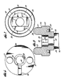
- FIG. 3 illustrates an exemplary lead frame for use in manufacturing DIPs suitable for an optical isolator as provided in practice of this invention.
- the lead frame comprises a pair of side rails 17 which may carry between them the electrical leads and supporting structure for making a plurality of DIPs in automated machinery.
- the portion of the lead frame illustrated in FIG. 3 is sufficient for making a pair of conventional eight-lead DIPs side by side. Several such pairs may be provided along the length of the side rails.
- One segment 18 of the lead frame provides the lower electrical leads for a pair of DIPs and an adjacent segment 19 provides the upper electrical leads for a pair of DIPs.
- a photodetector die 12 is fixed on one electrical lead in the bottom lead segment 18.
- an LED 14 is secured on an electrical lead in the upper lead segment 19.
- the ends of a tie bar 21 are sheared from the side rails and the array of leads in the upper segment 19 is rotated 180° by twisting hinge "pins" 22 connecting the array of leads to the side rails. This rotation (not illustrated herein) brings each LED to a carefully aligned position over the top of the corresponding photodetector die. As described in the '183 patent, this brings the LED into good alignment with the photodetector.
- the manufacturing technique for this invention differs from that described in the '183 patent in that before rotating the segment containing the LED, a light guide 23 (not shown in FIG. 3) is placed over or around the LED.
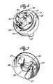
- a preferred light guide is illustrated apart from the other structure of the optical isolator in FIGS. 4 to 8.
- the light guide comprises a circular base or flange 25 which is flat on its top face 26, that is, the face that is mounted against the lead 11 supporting the LED.
- a pair of posts 27 extend from the flat face of the base.
- the light guide is assembled to the lead supporting the LED by passing the posts through holes (not shown) in the lead and then heat staking or upsetting the ends of the posts to form a bead 28 which secures the light guide and lead together.
- the base On its opposite face, the base has a circumferentially extending raised rim 29 around its perimeter.
- the rim is smoothly rounded and blends into an annular basin 31 inside the rim.
- a generally circular body 32 In the center of the basin there is a generally circular body 32 extending in the opposite direction from the mounting posts 27.
- One side portion of the body forms an extension 33 beyond a plane 34 forming the end of the principal portion of the body.
- the end 36 of the extension 33 is parallel to the flat face 26 of the base, and when the segment of upper leads is rotated to position over the lower leads, it rests against the lower lead, thereby providing a fixed spacing between the upper and lower leads.
- the height of the extension above the flat face of the base in an exemplary embodiment is 1.32 mm.
- the diameter of the base in such an embodiment is 2.29 mm.
- the plane 34 defines an end to the principal portion of the body so that there is a close spacing between the end of the body and a photodetector 12 beneath the light guide. Only a small gap is desirable between the light guide and photodetector for minimizing light loss and enhancing bonding to the molding material forming the body of the DIP. A gap as small as 75 micrometers or less is desirable.
- a generally cylindrical light passage extends through the light guide.
- a lower portion 38 of the light passage that is the portion nearer the photodiode, has a relatively smaller diameter and an upper portion 39 of the passage around the light emitting diode has a relatively larger diameter so that there is a step or shoulder 41 part way along the length of the light passage.
- a diagonally extending slit 42 between the flat face of the base and the larger diameter portion of the light passage provides clearance for lead wires to the LED.
- the passage through the light guide is slightly more than completely filled with an uncured silicone resin.
- the amount of resin added is only about 0.56 microliters.
- the silicone wets not only the interior of the light guide, but also the face of the photodetector.
- a narrow meniscus of silicone forms in the gap between the face of the photodetector and the plane 34 forming the end of the light guide.
- the light guide provides controlled spacing between the upper and lower leads. This, in combination with the known volume of the light passage, assures a fixed cavity volume so that a controlled amount of silicone resin may be added for complete filling. By carefully controlling the quantity of silicone resin placed in the passage, wetting of other surfaces of the light guide can be minimized. In the event of excess resin being added, the annular basin 31 surrounding the body of the light guide serves to catch overflow.
- a preferred silicone resin comprises mcGhan Nusil CV-8151, available from mcGhan Nusil Incorporated, Carpenteria, California. Another suitable resin may be Q1-4939 available from Dow Corning Corporation, Midland, Michigan. Each of these resins cures to form a viscous gel. It is important that the medium filling the light passage be highly transparent in the wavelength band of the optical isolator. It should also have high dielectric strength, be substantially free of bubbles, and wet the surfaces of the LED, light passage and photodetector. It should also be stable at the curing temperature of the molding material forming the body of the DIP.
- the body of the DIP is transfer molded by conventional techniques.
- An opaque insulating epoxy molding compound is typically transfer molded at about 70 kg per square centimeter. This has the incidental benefit of diminishing the size of any bubbles present in the silicone. It is important to have the optical path between the LED and photodetector filled with a transparent material; otherwise, the molding compound would intrude into the cavity and occult the photo detector.
- the epoxy is cured at elevated temperature, for example, 175 to 200 C. The leads can then be trimmed and bent to complete the DIP.
- the light guide is injection molded from high- temperature thermoplastic transparent, polyethersulfone resin such as Vitrex PES, available from Imperial Chemical Industries, Ltd, London, England.
- the polyethersulfone resin is loaded with 12% by weight of titanium dioxide pigment.
- Polyethersulfone is desirable since it has high dielectric strength, a linear coefficient of expansion similar to that of the epoxy transfer molding compound forming the body of the DIP, and a softening temperature greater than 200 C.
- the manufacturing technique can be summarized as follows:
- the light guide serves a number of functions. As suggested by the name given it herein, it serves to enhance the light flux from the LED which reaches the photodetector. This is not truly a "light guide" as one might think of it for fiber optics where there are differences in index of refraction to avoid loss of light from the sides of a guide. In some respects it is more like a reflective cavity and yet it differs from that as well.
- the actual mechanism for assuring excellent light transmission is not specular reflection, but rather it involves multiple scattering reflections in a closed cavity. This occurs since the polyethersulfone resin is transparent and light is reflected from the white titanium dioxide pigment. There is multiple scattering of light from the pigment which has a reflectivity of more than 85%. Because of this there is a large amount of scattering of light within the closed system with very little absorption. Penetration depth of light in the titanium dioxide loaded polyethersulfone is less than 500 micrometers.
- the wall thickness of the light guide should be less than 500 micrometers to avoid loss of light. It appears that light losses are less than about 10% in an exemplary embodiment.
- Metallic pigment in the resin might be more reflective, but such material is inappropriate because of the low conductivity required in the light guide to prevent electrical breakdown.
- the principal light loss appears to be due to light incident on the slit 42 which provides clearance for the LED lead wires. Reflections from the sloping wall leading away from the photodetector inefficiently return light to the principal light passage.
- Another important function of the light guide is to enhance the isolation voltage between the input and output.
- Several features of the light guide contribute to enhancing the electrical breakdown resistance.
- the light guide confines the silicone resin largely within the light passage so that wetting by the resin of other surfaces is minimized. This tends to minimize the presence of a "interlayer" of silicone resin in the interface between other structure and the insulating molding material forming the body of the DIP. Thus, only a narrow band at the gap adjacent to the photodetector is unwetted by the molding material. If any silicone does escape from the light passage it may be on a wall of the body or at most in the recessed basin 31 surrounding the body.
- the enlarged base 25 extending outwardly from the body of the light guide forms an insulating flange which increases the possible arc path along the surface of the light guide to a length significantly more the spacing between the upper and lower leads. It is observed that electrical breakdown commonly occurs along an interface such as along the surface of the light guide. By enlarging the path length along the surface of the light guide, higher breakdown voltages can be achieved. The somewhat crooked path along the outside surface of the light guide is more than the path length directly between the leads.
- the raised rounded peripheral rim 29 around the base contributes to forming an elongated crooked path along the surface of the light guide. In addition, it provides a surface which is approximately perpendicular to the electric field in the dielectric material between the conductive leads. This, too, enhances the resistance to electrical breakdown.
- the step or shoulder 41 in the light passage also provides a surface perpendicular to the electric field. As will be apparent, it also enlarges the path length along the interface between the polyethersulfone light guide and the silicone transparent medium within the light passage.
- optical isolator constructed according to principles of this invention to have an input-to-output isolation voltage of 5000 volts or more. Electrical breakdown voltage of as much as 12,000 volts may be obtained even though the spacing between the LED and the photodetector is as little as one-half millimeter.
- the entire assembly of light guide, transparent medium and molding material may be based on polyimide resins for even larger breakdown voltage resistance.
- Polyimide resins have very high inherent dielectric strength and are transparent in the wavelength bands of interest. Further, by making the entire assembly of similar resin, breakdown resistance along interfaces is enhanced.
- the light guide is molded of a transparent polyimide resin loaded with a white reflective pigment such as titanium dioxide. The resin may be only partly cured to a "B-stage" rather than completely cross-linked. Such a partly cured light guide may be secured to the electrical lead by heat deformation.
- the light passage is then filled with a transparent resin and the entire assembly embedded in a resin loaded with pigment to make it opaque.
- the resin within the light passage need not be cured before the final molding material is cured.
- the liquid polyimide resins bond well to the partially cured light guide to make an integral package of polyimide material with very high electrical breakdown resistance. Less attention needs to be directed to making crooked arc path lengths along the surfaces of the light guide in such an embodiment.
- optical isolator Although limited embodiments of optical isolator have been described and illustrated herein, many modifications and variations will be apparent to those skilled in the art. Thus, for example, a single optical isolator is provided in the DIP illustrated herein. If desired, more than one such optical isolator may be included in a single integrated circuit package. It will also be apparent that additional circuitry on integrated circuit chips, particul- ary for prccessing of the photodiode signal, may be included in the package.
- the light guide may, in effect, be reversed so that a photodetector is in a larger diameter portion of the light passage and an LED is in the smaller diameter portion. This should result in slightly less light loss due to the step in the passage. It will be noted that it immaterial whether the enlarged flange is adjacent to the photodetector lead or the LED lead. Voltage differences are all that are of concern. Further, the signals applied in many applications are alternating current.
- the features of the light guide provided in practice of this invention may be combined with mounting of an LED in an indented cup for further reflecting light toward the photodetector.
Landscapes
- Photo Coupler, Interrupter, Optical-To-Optical Conversion Devices (AREA)
Applications Claiming Priority (2)
| Application Number | Priority Date | Filing Date | Title |
|---|---|---|---|
| US355443 | 1989-05-22 | ||
| US07/355,443 US4980568A (en) | 1989-05-22 | 1989-05-22 | Optical isolator having high voltage isolation and high light flux light guide |
Publications (2)
| Publication Number | Publication Date |
|---|---|
| EP0399703A2 true EP0399703A2 (de) | 1990-11-28 |
| EP0399703A3 EP0399703A3 (de) | 1990-12-05 |
Family
ID=23397455
Family Applications (1)
| Application Number | Title | Priority Date | Filing Date |
|---|---|---|---|
| EP19900305084 Withdrawn EP0399703A3 (de) | 1989-05-22 | 1990-05-11 | Optischer Hochspannungsisolator |
Country Status (3)
| Country | Link |
|---|---|
| US (1) | US4980568A (de) |
| EP (1) | EP0399703A3 (de) |
| JP (1) | JPH036062A (de) |
Cited By (1)
| Publication number | Priority date | Publication date | Assignee | Title |
|---|---|---|---|---|
| WO2017122003A3 (en) * | 2016-01-12 | 2017-08-24 | Marcus Lewis | Isolation device |
Families Citing this family (36)
| Publication number | Priority date | Publication date | Assignee | Title |
|---|---|---|---|---|
| US5233208A (en) * | 1990-03-23 | 1993-08-03 | U.S. Philips Corp. | Photocoupler surrounded by transparent and reflective resins in a preformed pin housing |
| US5101465A (en) * | 1990-08-07 | 1992-03-31 | At&T Bell Laboratories | Leadframe-based optical assembly |
| US5329131A (en) * | 1991-05-17 | 1994-07-12 | U.S. Philips Corporation | Opto-electronic coupler having improved moisture protective housing |
| US5751009A (en) * | 1996-04-25 | 1998-05-12 | Motorola, Inc. | Optical isolator having leadframe with non-planar mounting portions |
| US6051848A (en) * | 1998-03-02 | 2000-04-18 | Motorola, Inc. | Optical device packages containing an optical transmitter die |
| US6376851B1 (en) * | 1998-09-21 | 2002-04-23 | Eugene Robert Worley | Opto-coupler applications suitable for low efficiency silicon based LEDs |
| US6931003B2 (en) * | 2000-02-09 | 2005-08-16 | Bookline Flolmstead Llc | Packet prioritization protocol for a large-scale, high speed computer network |
| US6897567B2 (en) * | 2000-07-31 | 2005-05-24 | Romh Co., Ltd. | Method of making wireless semiconductor device, and leadframe used therefor |
| JP4813691B2 (ja) * | 2001-06-06 | 2011-11-09 | シチズン電子株式会社 | 発光ダイオード |
| JP3802844B2 (ja) * | 2002-06-14 | 2006-07-26 | 古河電気工業株式会社 | 光半導体モジュール |
| US7072534B2 (en) * | 2002-07-22 | 2006-07-04 | Applied Materials, Inc. | Optical ready substrates |
| US7043106B2 (en) * | 2002-07-22 | 2006-05-09 | Applied Materials, Inc. | Optical ready wafers |
| US7110629B2 (en) | 2002-07-22 | 2006-09-19 | Applied Materials, Inc. | Optical ready substrates |
| US7084935B2 (en) * | 2002-08-28 | 2006-08-01 | Adaptive Micro Systems, Llc | Display device with molded light guide |
| WO2005001520A2 (en) * | 2003-05-29 | 2005-01-06 | Applied Materials, Inc. | Serial routing of optical signals |
| EP1649566A4 (de) * | 2003-06-27 | 2007-08-15 | Applied Materials Inc | Gepulstes quanten-dot-lasersystem mit niedrigem jitter |
| JP4282392B2 (ja) * | 2003-07-11 | 2009-06-17 | 株式会社東芝 | 光半導体装置及びその製造方法 |
| US20050016446A1 (en) | 2003-07-23 | 2005-01-27 | Abbott John S. | CaF2 lenses with reduced birefringence |
| DE10340816A1 (de) * | 2003-09-04 | 2005-03-31 | Robert Bosch Gmbh | Verfahren und Vorrichtung zum Betreiben einer Brennkraftmaschine |
| US7181919B2 (en) * | 2004-03-31 | 2007-02-27 | Denso Corporation | System utilizing waste heat of internal combustion engine |
| US20050281009A1 (en) * | 2004-06-17 | 2005-12-22 | Kokusan Denki Co., Ltd. | Electronic circuit unit for internal combustion engine |
| US20060222024A1 (en) * | 2005-03-15 | 2006-10-05 | Gray Allen L | Mode-locked semiconductor lasers with quantum-confined active region |
| US20060227825A1 (en) * | 2005-04-07 | 2006-10-12 | Nl-Nanosemiconductor Gmbh | Mode-locked quantum dot laser with controllable gain properties by multiple stacking |
| KR100689394B1 (ko) * | 2005-06-28 | 2007-03-02 | 삼성전자주식회사 | 휴대 장치용 키패드 어셈블리 |
| WO2007027615A1 (en) | 2005-09-01 | 2007-03-08 | Applied Materials, Inc. | Ridge technique for fabricating an optical detector and an optical waveguide |
| US7835408B2 (en) | 2005-12-07 | 2010-11-16 | Innolume Gmbh | Optical transmission system |
| WO2007065614A2 (en) * | 2005-12-07 | 2007-06-14 | Innolume Gmbh | Laser source with broadband spectrum emission |
| US7561607B2 (en) * | 2005-12-07 | 2009-07-14 | Innolume Gmbh | Laser source with broadband spectrum emission |
| US20070243844A1 (en) * | 2006-04-12 | 2007-10-18 | Nokia Corporation | Flexible optical illumination system |
| JP4897530B2 (ja) * | 2007-03-23 | 2012-03-14 | ルネサスエレクトロニクス株式会社 | フォトカプラおよびその組立方法 |
| TW201000806A (en) * | 2008-06-19 | 2010-01-01 | Lighthouse Technology Co Ltd | Light-emitting component and its forming mold |
| WO2010065731A2 (en) | 2008-12-03 | 2010-06-10 | Innolume Gmbh | Semiconductor laser with low relative intensity noise of individual longitudinal modes and optical transmission system incorporating the laser |
| US8265487B2 (en) * | 2009-07-29 | 2012-09-11 | Avago Technologies Fiber Ip (Singapore) Pte. Ltd. | Half-duplex, single-fiber (S-F) optical transceiver module and method |
| US9279946B2 (en) * | 2012-05-23 | 2016-03-08 | Avago Technologies General Ip (Singapore) Pte. Ltd. | Premolded cavity for optoelectronic device |
| TWI595518B (zh) | 2015-11-04 | 2017-08-11 | 財團法人工業技術研究院 | 電隔離器構裝結構及電隔離器的製造方法 |
| TWI573315B (zh) | 2016-01-19 | 2017-03-01 | 財團法人工業技術研究院 | 電隔離器電路 |
Family Cites Families (13)
| Publication number | Priority date | Publication date | Assignee | Title |
|---|---|---|---|---|
| DE2253699C3 (de) * | 1972-11-02 | 1978-11-23 | Licentia Patent-Verwaltungs-Gmbh, 6000 Frankfurt | Halbleiter-Optokoppler und Verfahren zu seiner Herstellung |
| FR2272377B1 (de) * | 1974-05-24 | 1977-06-24 | Texas Instruments France | |
| GB1557685A (en) * | 1976-02-02 | 1979-12-12 | Fairchild Camera Instr Co | Optically coupled isolator device |
| GB1564937A (en) * | 1976-12-13 | 1980-04-16 | Tokyo Shibaura Electric Co | Optoelectronic coupler |
| FR2388412A1 (fr) * | 1977-04-18 | 1978-11-17 | Radiotechnique Compelec | Element isolant pour dispositif optoelectronique photocoupleur et dispositifs comportant un tel element |
| DE2806167C2 (de) * | 1978-02-14 | 1986-05-15 | Siemens AG, 1000 Berlin und 8000 München | Hochspannungsfester Optokoppler |
| US4450461A (en) * | 1981-07-24 | 1984-05-22 | General Electric Company | Low cost high isolation voltage optocoupler with improved light transmissivity |
| US4446375A (en) * | 1981-10-14 | 1984-05-01 | General Electric Company | Optocoupler having folded lead frame construction |
| JPS6195581A (ja) * | 1984-10-16 | 1986-05-14 | Toshiba Corp | 光結合素子 |
| JPS61228681A (ja) * | 1985-04-01 | 1986-10-11 | Sharp Corp | 光結合半導体装置 |
| JPH0669040B2 (ja) * | 1985-05-13 | 1994-08-31 | 株式会社東芝 | 光半導体装置 |
| US4694183A (en) * | 1985-06-25 | 1987-09-15 | Hewlett-Packard Company | Optical isolator fabricated upon a lead frame |
| US4633582A (en) * | 1985-08-14 | 1987-01-06 | General Instrument Corporation | Method for assembling an optoisolator and leadframe therefor |
-
1989
- 1989-05-22 US US07/355,443 patent/US4980568A/en not_active Expired - Lifetime
-
1990
- 1990-05-11 EP EP19900305084 patent/EP0399703A3/de not_active Withdrawn
- 1990-05-22 JP JP2132403A patent/JPH036062A/ja active Pending
Cited By (1)
| Publication number | Priority date | Publication date | Assignee | Title |
|---|---|---|---|---|
| WO2017122003A3 (en) * | 2016-01-12 | 2017-08-24 | Marcus Lewis | Isolation device |
Also Published As
| Publication number | Publication date |
|---|---|
| US4980568A (en) | 1990-12-25 |
| JPH036062A (ja) | 1991-01-11 |
| EP0399703A3 (de) | 1990-12-05 |
Similar Documents
| Publication | Publication Date | Title |
|---|---|---|
| US4980568A (en) | Optical isolator having high voltage isolation and high light flux light guide | |
| US7446347B2 (en) | Optoelectronic component and method for the production thereof, module and device comprising a module of this type | |
| US4857746A (en) | Method for producing an optocoupler | |
| US7943951B2 (en) | Light emitting device package | |
| KR101160037B1 (ko) | 파워 표면 마운트 발광 다이 패키지 | |
| JP4180537B2 (ja) | 光学素子の封止構造体および光結合器ならびに光学素子の封止方法 | |
| US7775685B2 (en) | Power surface mount light emitting die package | |
| JP4945106B2 (ja) | 半導体発光装置 | |
| US8735931B2 (en) | Light emitting diode package and fabrication method thereof | |
| EP1537603B1 (de) | Oberflächenmontiertes gehäuse für lichtemittierenden leistungschip | |
| US20080180960A1 (en) | Lighting device package | |
| US8288183B2 (en) | Method of manufacturing an optically coupled device | |
| US4179619A (en) | Optocoupler having internal reflection and improved isolation capabilities | |
| CN101569023A (zh) | 用于光电子器件的壳体和光电子器件在壳体中的布置 | |
| TW201436294A (zh) | 具有成側向形態或頂向形態裝置定向之疊層無引線載架封裝的光電子裝置(一) | |
| EP2485284A1 (de) | Lichtemittierende vorrichtung | |
| JPH10144965A (ja) | 光半導体装置及びその製造方法 | |
| US9209338B2 (en) | Optical device with through-hole cavity | |
| EP2503609A2 (de) | Gehäuse mit lichtemittierender Vorrichtung | |
| US20040149995A1 (en) | Photo-coupler semiconductor device and production method therefor | |
| JP2000173947A (ja) | プラスティックパッケージ | |
| US7928466B2 (en) | Light emitting semi-conductor diode (with high light output) | |
| US7736070B2 (en) | Double mold optocoupler | |
| EP4443123B1 (de) | Überwachungsvorrichtung für ein halbleiterbauelement, halbleiterbauelement und verfahren zur herstellung davon | |
| KR101161397B1 (ko) | 실리콘 렌즈를 구비하는 발광소자 및 그것을 제조하는 방법 |
Legal Events
| Date | Code | Title | Description |
|---|---|---|---|
| PUAI | Public reference made under article 153(3) epc to a published international application that has entered the european phase |
Free format text: ORIGINAL CODE: 0009012 |
|
| PUAL | Search report despatched |
Free format text: ORIGINAL CODE: 0009013 |
|
| AK | Designated contracting states |
Kind code of ref document: A2 Designated state(s): DE FR GB IT |
|
| AK | Designated contracting states |
Kind code of ref document: A3 Designated state(s): DE FR GB IT |
|
| 17P | Request for examination filed |
Effective date: 19910521 |
|
| 17Q | First examination report despatched |
Effective date: 19930316 |
|
| STAA | Information on the status of an ep patent application or granted ep patent |
Free format text: STATUS: THE APPLICATION IS DEEMED TO BE WITHDRAWN |
|
| 18D | Application deemed to be withdrawn |
Effective date: 19951010 |