EP0400363B1 - Soudure tendre à température de fusion basse, dopée au cuivre, pour le montage et le remontage de composants - Google Patents
Soudure tendre à température de fusion basse, dopée au cuivre, pour le montage et le remontage de composants Download PDFInfo
- Publication number
- EP0400363B1 EP0400363B1 EP90108688A EP90108688A EP0400363B1 EP 0400363 B1 EP0400363 B1 EP 0400363B1 EP 90108688 A EP90108688 A EP 90108688A EP 90108688 A EP90108688 A EP 90108688A EP 0400363 B1 EP0400363 B1 EP 0400363B1
- Authority
- EP
- European Patent Office
- Prior art keywords
- copper
- solder
- tin
- rework
- soldering
- Prior art date
- Legal status (The legal status is an assumption and is not a legal conclusion. Google has not performed a legal analysis and makes no representation as to the accuracy of the status listed.)
- Expired - Lifetime
Links
Images

Classifications
-
- B—PERFORMING OPERATIONS; TRANSPORTING
- B23—MACHINE TOOLS; METAL-WORKING NOT OTHERWISE PROVIDED FOR
- B23K—SOLDERING OR UNSOLDERING; WELDING; CLADDING OR PLATING BY SOLDERING OR WELDING; CUTTING BY APPLYING HEAT LOCALLY, e.g. FLAME CUTTING; WORKING BY LASER BEAM
- B23K35/00—Rods, electrodes, materials, or media, for use in soldering, welding, or cutting
- B23K35/22—Rods, electrodes, materials, or media, for use in soldering, welding, or cutting characterised by the composition or nature of the material
-
- H—ELECTRICITY
- H05—ELECTRIC TECHNIQUES NOT OTHERWISE PROVIDED FOR
- H05K—PRINTED CIRCUITS; CASINGS OR CONSTRUCTIONAL DETAILS OF ELECTRIC APPARATUS; MANUFACTURE OF ASSEMBLAGES OF ELECTRICAL COMPONENTS
- H05K3/00—Apparatus or processes for manufacturing printed circuits
- H05K3/30—Assembling printed circuits with electric components, e.g. with resistors
- H05K3/32—Assembling printed circuits with electric components, e.g. with resistors electrically connecting electric components or wires to printed circuits
- H05K3/34—Assembling printed circuits with electric components, e.g. with resistors electrically connecting electric components or wires to printed circuits by soldering
- H05K3/346—Solder materials or compositions specially adapted therefor
-
- B—PERFORMING OPERATIONS; TRANSPORTING
- B23—MACHINE TOOLS; METAL-WORKING NOT OTHERWISE PROVIDED FOR
- B23K—SOLDERING OR UNSOLDERING; WELDING; CLADDING OR PLATING BY SOLDERING OR WELDING; CUTTING BY APPLYING HEAT LOCALLY, e.g. FLAME CUTTING; WORKING BY LASER BEAM
- B23K35/00—Rods, electrodes, materials, or media, for use in soldering, welding, or cutting
- B23K35/22—Rods, electrodes, materials, or media, for use in soldering, welding, or cutting characterised by the composition or nature of the material
- B23K35/24—Selection of soldering or welding materials proper
- B23K35/26—Selection of soldering or welding materials proper with the principal constituent melting at less than 400°C
- B23K35/262—Sn as the principal constituent
-
- C—CHEMISTRY; METALLURGY
- C22—METALLURGY; FERROUS OR NON-FERROUS ALLOYS; TREATMENT OF ALLOYS OR NON-FERROUS METALS
- C22C—ALLOYS
- C22C13/00—Alloys based on tin
Definitions
- This invention relates to a composition of solder suitable for low temperature soldering of printed circuit boards.
- Component assembly and reassembly, or rework, on a printed circuit board using a fountain process is conventionally performed by pumping a liquified solder through a chimney, which attaches the component or connector to the printed circuit board by means of a through hole.
- a wave solder technique or solder pen may be used.
- the walls of the through holes of a circuit board are typically coated with copper metal which makes an electrical contact between at least two levels of circuitry.
- Components can be mounted onto the circuit board by means of inserting and soldering pins into through holes.
- the composition of the solder is determinant of the temperature required to liquify the solder and thus perform the rework. This temperature is typically about 50°C above the liquidus temperature of the solder composition.
- the solder flow rate should be kept to a minimum such that the solder remains in the region where it is desired rather than flowing beyond.
- the soldering time should also be kept to a minimum. The precaution of minimizing temperature, soldering time and flow rate is intended to contribute to minimizing the dissolution of copper from the walls of the conductive through hole into the solder.
- solder is the high melt eutectic 63 wt. % Sn/37 wt. % Pb, which liquifies at 183°C.
- high temperature soldering contributes to degradation of the organic resins in the laminate, and may produce delamination and distortion in the localized area of the reworked component.
- This invention therefore relates to a composition of low temperature solder comprising tin, in which is also present a dopant level of copper in an amount below the binary tin-copper eutectic point.
- the new solder may be applied to the material to be soldered using solder fountain and other conventional soldering techniques. Because of its low melting point relative to other copper containing solders, the new solder may be used for nondestructive soldering of materials not amenable to being soldered by copper containing solders available heretofore.
- this invention relates to a composition of copper doped low temperature solder suitable for use in component assembly and rework on printed circuit cards or boards.
- solders have been devised for a number of specific applications, such as to wet and bond to carbon and semiconductors (US-A-4 512 950 to Hosoda et al, issued April 23, 1985 and US-A-4 396 677 to Intrater, issued August 2, 1983), to inhibit the formation of oxide (US-A-4 654 275 to Bose, issued March 31, 1987, to increase tensile strength (US-A-4 588 657 to Kujas, issued May 13, 1986), to soft solder aluminum (US-A-4 070 192 to Arbib et al, issued January 24, 1978, to bond semiconductor to metal (US-A-4 357 162 to Guan, issued November 2, 1982), to bond oxide surfaces using vibration (US-A-4 106 930 to Nomaki et al, issued August 15, 1978), to solder joints for lead-free potable water (US-A-4 695 428 to Ball
- the problem which is solved by the present invention is quite different: how to assemble and rework a through hole connection in a printed circuit device in such a manner that the dissolution of a copper coating on the walls of the through hole connection into the solder is suppressed. Rework is reflowing the solder in the joint.
- the '844 patent described that it was "essential that an eutectic of tin and copper should form in the (solder) alloy", that eutectic consisting of 99% Sn and 1% Cu (see column 2, lines 30-37). It also described that whatever the amount of copper in the solder, it should be minimally sufficient to form this binary tin-copper eutectic point. Thus in a 50/50 Pb/Sn solder, Cu in the amount of 0.5% of the total weight of the solder should be added.
- Copper containing solder has been obtainable on the marketplace since at least about 1964, the publication date of Solders and Soldering , pp. 65-66 McGraw-Hill Book Co., H. H. Manko. However, this reference does not give specific compositions of commercially available copper containing solders, saying only that the amount is "high".
- Savbit 1 alloy obtainable from Multicore of Westbury, NY, comprising about 1.5% to about 2.0% Cu by weight, has been used to extend the life of copper soldering tips in static hand soldering applications.
- Product data sheets recommend a minimum bit temperature of 272-294°C, above the range required for nondestructive assemblies and rework on printed circuit boards and cards.
- the present invention as claimed is directed to a novel solder composition which retards the dissolution of copper within and surrounding a through hole or blind via and operates at a lower temperature than before possible with available copper containing solders, permitting assembly and repeated rework of faulty solder connections in and around the through holes of printed circuit boards while also avoiding other problems associated with higher temperature rework, such as delamination of layers in the laminate board, localized mechanical distortion, and degeneration of solder joints and exceeding the critical temperature of the mounted device.
- doping solder comprising tin to contain non-zero levels of copper in amounts below the binary tin-copper eutectic point composition significantly reduces the amount of copper dissolution from the walls of through holes into the copper doped solder during assembly and rework while not degrading the solderability of the solder or increasing the soldering temperature.
- this effect occurs in a copper containing tin solder having a soldering temperature low enough to avoid delamination or other temperature related degradation within multilevel circuit board assemblies and provide good fatigue properties.
- Below the binary tin-copper eutectic point is defined as 99.1 wt. % Sn 0.9 wt. % Cu to 100 wt. % Sn as defined on page 299 of Metallography, Structures and Phase Diagrams , by the American Society for Metals.
- solder compositions within the following ranges would be effective for this purpose; a trace amount meaning .02 wt. %, an amount that may be present without being added, or which lies within the lowest error range. Trace amounts are inconsequential in effect.
- tin 53 to 55% by weight lead 25 to 27% by weight indium 18 to 22% by weight copper above trace amounts to 0.50% by weight, the amount in a particular instance selected to be below the binary tin-copper eutectic point.
- the following nominal composition is likewise effective: tin 54% by weight lead 26% by weight indium 20% by weight copper in an amount above trace amounts selected to be below the binary tin-copper eutectic point.
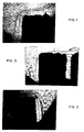
- Figure 1 shows in cross-section one corner of a copper plated through hole which has been soldered with nominal 54 tin/26 lead/20 indium low melt solder, but has not undergone rework. Magnification is 800X.
- Figure 2 shows in cross-section one corner of a copper plated through hole after four reworks with a solder of essentially the same nominal composition as shown in Figure 1, but doped to contain 0.14 wt. % Cu. Magnification is 800X.
- Figure 3 shows in cross-section one corner of a copper plated through hole after four reworks with a solder being the same composition as the solder shown in Figure 1.
- the black areas of the figures are the dielectric of the circuit board.
- the layered intermediate areas are plated copper.
- the grayish area is the solder.
- the through hole has been soldered but has undergone no rework.
- the through hole has undergone four cycles of rework and the plated copper layer is no longer electrically continuous.
- the through hole of Figure 2 has, like Figure 3, undergone four cycles of rework, the difference being that solder used in Figure 2 is copper doped, and the plated copper layer is still electrically continuous.
- a copper plated through hole which has undergone four reworks with conventional undoped Pb/Sn solder shows substantially no copper remaining on the through-hole walls.
- Figure 4 shows the copper thickness dissolved from the walls of through holes which were exposed to a ternary solder doped with copper in amounts below the binary tin-copper eutectic point, 0.10 weight percent to 0.20 weight percent.
- the nominal composition of the ternary solder in ratios of weight percent was 54 tin/26 lead/20 indium, plus the copper dopant.
- the figure also shows for comparison purposes the amount of copper dissolved into virgin, i.e. undoped, solder.
- the data were obtained in the following manner: Time zero control measurements were taken on raw cards via metallographic cross sectioning. There were four raw card technologies and eight different components to represent a worst case product hardware test. Each component was reworked on a solder fountain the maximum amount required for each card technology.
- solder contact time was kept the same for each component and varied slightly for different component type with the total solder contact time up to about 200 seconds.
- Final measurements (after maximum number of reworks) were taken via metallographic cross sectioning within the module site and in the adjacent plated through holes next to the module site. All data points were averaged for each module site. All averaged module site data points were averaged for each module type. The averaged final measurements were subtracted from the averaged initial measurements to determine the averaged amount of copper dissolved. These values were averaged with all components for each of the copper levels and plotted on a "Copper Dissolved vs. % Copper in Solder" graph.
- Photomicrographs at time zero, and after four reworks with virgin solder and after four reworks with 0.14% copper doped solder depict the advantage of copper doping.
- the figure indicates that in the ternary solders discussed above, the amount of copper dissolved drops dramatically with the addition of copper dopant and continues to drop as more dopant is added, up to the limit tested.
- composition of the present invention has been effective in soldering and reworking copper coated circuit boards, it is equally applicable to soldering any material that comprises copper and for which low temperature soldering is desirable or necessary.
Landscapes
- Engineering & Computer Science (AREA)
- Mechanical Engineering (AREA)
- Manufacturing & Machinery (AREA)
- Microelectronics & Electronic Packaging (AREA)
- Chemical & Material Sciences (AREA)
- Materials Engineering (AREA)
- Metallurgy (AREA)
- Organic Chemistry (AREA)
- Electric Connection Of Electric Components To Printed Circuits (AREA)
- Arc Welding In General (AREA)
- Manufacturing Of Printed Wiring (AREA)
Claims (2)
- Composé de soudure à l'étain adapté pour le soudage à l'étain à basses températures de cartes à circuits imprimés conçu pour empêcher la dissolution du cuivre au cours du soudage et pour permettre l'apport de retouches aux composants électroniques enrobés de cuivre ou contenant du cuivre, à base d'étain, de plomb et d'indium, et de cuivre comme agent de dopage, dans lequel la teneur en cuivre (en pourcentage du poids) est comprise entre au moins 0,02% et au plus 0,9% et les teneurs en étain, plomb et indium sont comprises dans les plages suivantes (en pourcentage du poids) :
étain 53% à 55% plomb 25% à 27% indium 18% à 22% - Composé de soudure à l'étain selon la revendication 1, dans lequel la soudure est normalement composée de 54% d'étain / 26% de plomb / 20% d'indium en pourcentage du poids, et dopée avec 0,12 à 0,20% de cuivre en pourcentage du poids.
Applications Claiming Priority (2)
| Application Number | Priority Date | Filing Date | Title |
|---|---|---|---|
| US07/359,315 US5011658A (en) | 1989-05-31 | 1989-05-31 | Copper doped low melt solder for component assembly and rework |
| US359315 | 1989-05-31 |
Publications (2)
| Publication Number | Publication Date |
|---|---|
| EP0400363A1 EP0400363A1 (fr) | 1990-12-05 |
| EP0400363B1 true EP0400363B1 (fr) | 1995-03-08 |
Family
ID=23413297
Family Applications (1)
| Application Number | Title | Priority Date | Filing Date |
|---|---|---|---|
| EP90108688A Expired - Lifetime EP0400363B1 (fr) | 1989-05-31 | 1990-05-09 | Soudure tendre à température de fusion basse, dopée au cuivre, pour le montage et le remontage de composants |
Country Status (12)
| Country | Link |
|---|---|
| US (1) | US5011658A (fr) |
| EP (1) | EP0400363B1 (fr) |
| JP (1) | JP2825001B2 (fr) |
| KR (1) | KR930001686B1 (fr) |
| CN (1) | CN1022813C (fr) |
| AU (1) | AU617615B2 (fr) |
| BR (1) | BR9002559A (fr) |
| CA (1) | CA2000301C (fr) |
| DE (1) | DE69017516T2 (fr) |
| ES (1) | ES2069622T3 (fr) |
| HK (1) | HK203696A (fr) |
| PH (1) | PH27381A (fr) |
Families Citing this family (20)
| Publication number | Priority date | Publication date | Assignee | Title |
|---|---|---|---|---|
| JP2891432B2 (ja) * | 1989-12-27 | 1999-05-17 | 田中電子工業株式会社 | 半導体材料の接続方法,それに用いる接続材料及び半導体装置 |
| US5316788A (en) * | 1991-07-26 | 1994-05-31 | International Business Machines Corporation | Applying solder to high density substrates |
| US5520752A (en) * | 1994-06-20 | 1996-05-28 | The United States Of America As Represented By The Secretary Of The Army | Composite solders |
| CA2214130C (fr) * | 1996-09-19 | 2003-12-02 | Northern Telecom Limited | Ensembles de substrats et de composants electroniques |
| US6280584B1 (en) | 1998-07-29 | 2001-08-28 | Applied Materials, Inc. | Compliant bond structure for joining ceramic to metal |
| US6221514B1 (en) * | 1999-08-30 | 2001-04-24 | Delphi Technologies, Inc. | High-current circuit trace and composition and method therefor |
| US6216938B1 (en) * | 1999-09-30 | 2001-04-17 | International Business Machines Corporation | Machine and process for reworking circuit boards |
| US6490144B1 (en) | 1999-11-29 | 2002-12-03 | Applied Materials, Inc. | Support for supporting a substrate in a process chamber |
| US6892925B2 (en) * | 2002-09-18 | 2005-05-17 | International Business Machines Corporation | Solder hierarchy for lead free solder joint |
| US6854636B2 (en) * | 2002-12-06 | 2005-02-15 | International Business Machines Corporation | Structure and method for lead free solder electronic package interconnections |
| US7309647B1 (en) * | 2003-03-05 | 2007-12-18 | Altera Corporation | Method of mounting an electroless nickel immersion gold flip chip package |
| US7111771B2 (en) * | 2003-03-31 | 2006-09-26 | Intel Corporation | Solders with surfactant-refined grain sizes, solder bumps made thereof, and methods of making same |
| US6917113B2 (en) * | 2003-04-24 | 2005-07-12 | International Business Machines Corporatiion | Lead-free alloys for column/ball grid arrays, organic interposers and passive component assembly |
| US7005745B2 (en) | 2004-01-22 | 2006-02-28 | Texas Instruments Incorporated | Method and structure to reduce risk of gold embrittlement in solder joints |
| US20060113683A1 (en) * | 2004-09-07 | 2006-06-01 | Nancy Dean | Doped alloys for electrical interconnects, methods of production and uses thereof |
| US20060226199A1 (en) * | 2005-03-30 | 2006-10-12 | Visteon Global Technologies, Inc. | Selective soldering of flat flexible cable with lead-free solder to a substrate |
| US20070138442A1 (en) * | 2005-12-19 | 2007-06-21 | Weiser Martin W | Modified and doped solder alloys for electrical interconnects, methods of production and uses thereof |
| CN103697317A (zh) * | 2013-12-17 | 2014-04-02 | 中山名创力电子有限公司 | 一种由焊接不良材料制成的电子焊接件 |
| CN107845698A (zh) * | 2016-09-19 | 2018-03-27 | 无锡市斯威克科技有限公司 | 高效预涂锡反光焊带 |
| CN108161272A (zh) * | 2018-01-30 | 2018-06-15 | 无锡市斯威克科技有限公司 | 一种专用于超薄光伏电池片焊接的低熔点焊带及制备方法 |
Family Cites Families (27)
| Publication number | Priority date | Publication date | Assignee | Title |
|---|---|---|---|---|
| US2471899A (en) * | 1940-07-08 | 1949-05-31 | Spolek | Method of separating constituents of alloys by fractional crystallization |
| US2243278A (en) * | 1940-11-09 | 1941-05-27 | Johnson John | Alloy for soldering aluminum |
| US2303193A (en) * | 1941-10-04 | 1942-11-24 | Bell Telephone Labor Inc | Alloy |
| GB601029A (en) * | 1945-06-20 | 1948-04-26 | William Martin | An improved aluminium solder |
| US2501859A (en) * | 1947-10-22 | 1950-03-28 | Western Electric Co | Spacer or mold surface for the vulcanization of rubber |
| US2671844A (en) * | 1951-07-26 | 1954-03-09 | Guenther W Laubmeyer | Tin solder |
| DE1204500B (de) * | 1960-08-02 | 1965-11-04 | Dr G Laubmeyer | Verwendung von Zinn-Blei-Legierungen als Weichlot zum automatischen Tauchloeten |
| JPS4218219B1 (fr) * | 1965-05-12 | 1967-09-20 | ||
| US3650735A (en) * | 1969-04-04 | 1972-03-21 | Luigi Monaco | Tin base alloy containing aluminum, zinc and copper |
| US3607252A (en) * | 1969-06-02 | 1971-09-21 | Sperry Rand Corp | Solder alloy composition |
| GB1294801A (en) * | 1970-09-17 | 1972-11-01 | Ibm | Tin, lead and indium alloys |
| US4106930A (en) * | 1972-02-19 | 1978-08-15 | Asahi Glass Company, Ltd. | Solder alloys for soldering difficultly solderable material |
| FR2282319A1 (fr) * | 1974-08-19 | 1976-03-19 | Multicore Solders Ltd | Composition de soudage a flux et procede de soudure |
| JPS5154056A (ja) * | 1974-11-08 | 1976-05-12 | Hitachi Ltd | Handagokin |
| GB1461371A (en) * | 1975-02-19 | 1977-01-13 | Glacier Metal Co Ltd | Bearing alloys |
| US4357162A (en) * | 1979-10-04 | 1982-11-02 | Motorola, Inc. | Solder composition |
| US4396677A (en) * | 1980-10-24 | 1983-08-02 | Josef Intrater | Metal, carbon, carbide and other composites thereof |
| JPS58151037A (ja) * | 1982-03-02 | 1983-09-08 | Mitsubishi Metal Corp | 半導体装置用pb合金ろう材 |
| JPS60166191A (ja) * | 1984-02-06 | 1985-08-29 | Nippon Handa Kogyo Kk | 耐疲労特性にすぐれたはんだ合金 |
| GB2158459A (en) * | 1984-05-05 | 1985-11-13 | Imi Yorkshire Imperial Limited | Solder |
| US4588657A (en) * | 1984-11-01 | 1986-05-13 | Rca Corporation | Solder composition |
| US4622205A (en) * | 1985-04-12 | 1986-11-11 | Ibm Corporation | Electromigration lifetime increase of lead base alloys |
| JPS6272496A (ja) * | 1985-09-26 | 1987-04-03 | Matsuo Handa Kk | はんだ合金 |
| US4654275A (en) * | 1985-11-27 | 1987-03-31 | Allied Corporation | Storage life of Pb-In-Ag solder foil by Sn addition |
| US4695428A (en) * | 1986-08-21 | 1987-09-22 | J. W. Harris Company | Solder composition |
| JP2529257B2 (ja) * | 1987-04-22 | 1996-08-28 | 住友電気工業株式会社 | ヒユ−ズ用導体 |
| JPS63270437A (ja) * | 1987-04-24 | 1988-11-08 | Sumitomo Electric Ind Ltd | ヒユ−ズ用導体 |
-
1989
- 1989-05-31 US US07/359,315 patent/US5011658A/en not_active Expired - Lifetime
- 1989-10-06 CA CA002000301A patent/CA2000301C/fr not_active Expired - Fee Related
-
1990
- 1990-04-26 KR KR1019900005885A patent/KR930001686B1/ko not_active Expired - Fee Related
- 1990-05-03 PH PH40472A patent/PH27381A/en unknown
- 1990-05-09 DE DE69017516T patent/DE69017516T2/de not_active Expired - Lifetime
- 1990-05-09 EP EP90108688A patent/EP0400363B1/fr not_active Expired - Lifetime
- 1990-05-09 ES ES90108688T patent/ES2069622T3/es not_active Expired - Lifetime
- 1990-05-14 CN CN90102758A patent/CN1022813C/zh not_active Expired - Lifetime
- 1990-05-15 AU AU55052/90A patent/AU617615B2/en not_active Ceased
- 1990-05-30 BR BR909002559A patent/BR9002559A/pt active Search and Examination
- 1990-05-31 JP JP2140166A patent/JP2825001B2/ja not_active Expired - Fee Related
-
1996
- 1996-11-07 HK HK203696A patent/HK203696A/en not_active IP Right Cessation
Also Published As
| Publication number | Publication date |
|---|---|
| JPH0318497A (ja) | 1991-01-28 |
| HK203696A (en) | 1996-11-15 |
| PH27381A (en) | 1993-06-21 |
| DE69017516D1 (de) | 1995-04-13 |
| AU617615B2 (en) | 1991-11-28 |
| AU5505290A (en) | 1990-12-06 |
| KR930001686B1 (ko) | 1993-03-11 |
| JP2825001B2 (ja) | 1998-11-18 |
| US5011658A (en) | 1991-04-30 |
| CA2000301C (fr) | 1996-02-06 |
| KR900017721A (ko) | 1990-12-19 |
| ES2069622T3 (es) | 1995-05-16 |
| EP0400363A1 (fr) | 1990-12-05 |
| BR9002559A (pt) | 1991-08-13 |
| CA2000301A1 (fr) | 1990-11-30 |
| CN1047639A (zh) | 1990-12-12 |
| CN1022813C (zh) | 1993-11-24 |
| DE69017516T2 (de) | 1995-10-05 |
Similar Documents
| Publication | Publication Date | Title |
|---|---|---|
| EP0400363B1 (fr) | Soudure tendre à température de fusion basse, dopée au cuivre, pour le montage et le remontage de composants | |
| JP4613823B2 (ja) | ソルダペーストおよびプリント基板 | |
| EP1088615B1 (fr) | Brasure Sn-Ag-Cu et méthodes de traitement de surface et de montage de pièces l'utilisant | |
| EP0787559A1 (fr) | Alliage de soudage, soudure en pâte et procédé de soudage tendre | |
| US5942185A (en) | Lead-free solder used for connecting electronic parts on organic substrate and electronic products made using same | |
| EP2275224A1 (fr) | Alliage de brasage sans plomb ayant une apparition de cavité de retrait supprimée | |
| GB2346380A (en) | Nickel containing tin-based solder alloys | |
| CN1400081A (zh) | 无铅焊料合金 | |
| JP2005517535A (ja) | 無鉛すず−銀−銅合金はんだ組成物 | |
| EP1298726A2 (fr) | Composition de soudure pour des bosses sur semi-conducteurs | |
| US4941929A (en) | Solder paste formulation containing stannous fluoride | |
| KR20000070612A (ko) | 무연 주석 합금 | |
| EP1402989B1 (fr) | Alliage de soudage résistant au lessivage pour les films conducteurs épais à base d'argent | |
| JP3446517B2 (ja) | Pbフリーはんだ材料及びそれを用いた電子機器 | |
| JP2001168519A (ja) | 混載実装構造体及び混載実装方法並びに電子機器 | |
| KR930002154B1 (ko) | 땜납합금을 사용한 전자 회로장치 | |
| EP4667148A1 (fr) | Alliage de soudure, bille de soudure, pâte de soudure et joint soudé | |
| JP2004167569A (ja) | 無鉛はんだペースト組成物およびはんだ付け方法 | |
| JP2910527B2 (ja) | 高温はんだ | |
| JPH07246493A (ja) | はんだ合金 | |
| JP2004122223A (ja) | 電子部品および電子部品の製造方法 | |
| Strauss et al. | Low temperature soldering | |
| WO2006020769A1 (fr) | Procede et dispositif de fixation semi-conductrice | |
| KR100460957B1 (ko) | 무연 합금 솔더의 솔더링 플럭스 | |
| JPH07299585A (ja) | はんだ合金 |
Legal Events
| Date | Code | Title | Description |
|---|---|---|---|
| PUAI | Public reference made under article 153(3) epc to a published international application that has entered the european phase |
Free format text: ORIGINAL CODE: 0009012 |
|
| AK | Designated contracting states |
Kind code of ref document: A1 Designated state(s): CH DE ES FR GB IT LI NL SE |
|
| 17P | Request for examination filed |
Effective date: 19901213 |
|
| 17Q | First examination report despatched |
Effective date: 19930429 |
|
| GRAA | (expected) grant |
Free format text: ORIGINAL CODE: 0009210 |
|
| AK | Designated contracting states |
Kind code of ref document: B1 Designated state(s): CH DE ES FR GB IT LI NL SE |
|
| REF | Corresponds to: |
Ref document number: 69017516 Country of ref document: DE Date of ref document: 19950413 |
|
| REG | Reference to a national code |
Ref country code: ES Ref legal event code: FG2A Ref document number: 2069622 Country of ref document: ES Kind code of ref document: T3 |
|
| PGFP | Annual fee paid to national office [announced via postgrant information from national office to epo] |
Ref country code: SE Payment date: 19950519 Year of fee payment: 6 |
|
| ITF | It: translation for a ep patent filed | ||
| PGFP | Annual fee paid to national office [announced via postgrant information from national office to epo] |
Ref country code: ES Payment date: 19950523 Year of fee payment: 6 |
|
| PGFP | Annual fee paid to national office [announced via postgrant information from national office to epo] |
Ref country code: NL Payment date: 19950531 Year of fee payment: 6 |
|
| ET | Fr: translation filed | ||
| PLBE | No opposition filed within time limit |
Free format text: ORIGINAL CODE: 0009261 |
|
| STAA | Information on the status of an ep patent application or granted ep patent |
Free format text: STATUS: NO OPPOSITION FILED WITHIN TIME LIMIT |
|
| 26N | No opposition filed | ||
| PG25 | Lapsed in a contracting state [announced via postgrant information from national office to epo] |
Ref country code: ES Free format text: LAPSE BECAUSE OF NON-PAYMENT OF DUE FEES Effective date: 19960510 Ref country code: SE Effective date: 19960510 |
|
| PG25 | Lapsed in a contracting state [announced via postgrant information from national office to epo] |
Ref country code: NL Effective date: 19961201 |
|
| EUG | Se: european patent has lapsed |
Ref document number: 90108688.4 |
|
| NLV4 | Nl: lapsed or anulled due to non-payment of the annual fee |
Effective date: 19961201 |
|
| PGFP | Annual fee paid to national office [announced via postgrant information from national office to epo] |
Ref country code: CH Payment date: 19980828 Year of fee payment: 9 |
|
| REG | Reference to a national code |
Ref country code: ES Ref legal event code: FD2A Effective date: 19990301 |
|
| PG25 | Lapsed in a contracting state [announced via postgrant information from national office to epo] |
Ref country code: CH Free format text: LAPSE BECAUSE OF NON-PAYMENT OF DUE FEES Effective date: 19990531 Ref country code: LI Free format text: LAPSE BECAUSE OF NON-PAYMENT OF DUE FEES Effective date: 19990531 |
|
| REG | Reference to a national code |
Ref country code: CH Ref legal event code: PL |
|
| REG | Reference to a national code |
Ref country code: GB Ref legal event code: IF02 |
|
| PGFP | Annual fee paid to national office [announced via postgrant information from national office to epo] |
Ref country code: FR Payment date: 20020516 Year of fee payment: 13 |
|
| PG25 | Lapsed in a contracting state [announced via postgrant information from national office to epo] |
Ref country code: FR Free format text: LAPSE BECAUSE OF NON-PAYMENT OF DUE FEES Effective date: 20040130 |
|
| REG | Reference to a national code |
Ref country code: FR Ref legal event code: ST |
|
| PGFP | Annual fee paid to national office [announced via postgrant information from national office to epo] |
Ref country code: IT Payment date: 20060531 Year of fee payment: 17 |
|
| REG | Reference to a national code |
Ref country code: GB Ref legal event code: 746 Effective date: 20080416 |
|
| PGFP | Annual fee paid to national office [announced via postgrant information from national office to epo] |
Ref country code: DE Payment date: 20090528 Year of fee payment: 20 |
|
| PG25 | Lapsed in a contracting state [announced via postgrant information from national office to epo] |
Ref country code: IT Free format text: LAPSE BECAUSE OF NON-PAYMENT OF DUE FEES Effective date: 20070509 |
|
| PGFP | Annual fee paid to national office [announced via postgrant information from national office to epo] |
Ref country code: GB Payment date: 20090519 Year of fee payment: 20 |
|
| REG | Reference to a national code |
Ref country code: GB Ref legal event code: PE20 Expiry date: 20100508 |
|
| PG25 | Lapsed in a contracting state [announced via postgrant information from national office to epo] |
Ref country code: GB Free format text: LAPSE BECAUSE OF EXPIRATION OF PROTECTION Effective date: 20100508 |
|
| PG25 | Lapsed in a contracting state [announced via postgrant information from national office to epo] |
Ref country code: DE Free format text: LAPSE BECAUSE OF EXPIRATION OF PROTECTION Effective date: 20100509 |