EP0400397A2 - Procédé de synchronisation d'une horloge engendré à l'aide d'un compteur sur une horloge de référence - Google Patents
Procédé de synchronisation d'une horloge engendré à l'aide d'un compteur sur une horloge de référence Download PDFInfo
- Publication number
- EP0400397A2 EP0400397A2 EP90109250A EP90109250A EP0400397A2 EP 0400397 A2 EP0400397 A2 EP 0400397A2 EP 90109250 A EP90109250 A EP 90109250A EP 90109250 A EP90109250 A EP 90109250A EP 0400397 A2 EP0400397 A2 EP 0400397A2
- Authority
- EP
- European Patent Office
- Prior art keywords
- clock
- reference clock
- counter
- synchronization
- window
- Prior art date
- Legal status (The legal status is an assumption and is not a legal conclusion. Google has not performed a legal analysis and makes no representation as to the accuracy of the status listed.)
- Granted
Links
- 238000000034 method Methods 0.000 title claims abstract description 9
- 230000001360 synchronised effect Effects 0.000 claims abstract description 6
- 230000005540 biological transmission Effects 0.000 claims description 2
- 230000010363 phase shift Effects 0.000 abstract 1
- 230000000630 rising effect Effects 0.000 description 3
- 101000596093 Homo sapiens Transcription initiation factor TFIID subunit 1 Proteins 0.000 description 2
- 102100035222 Transcription initiation factor TFIID subunit 1 Human genes 0.000 description 2
- 102100034088 40S ribosomal protein S4, X isoform Human genes 0.000 description 1
- 101100350613 Arabidopsis thaliana PLL1 gene Proteins 0.000 description 1
- 101100082028 Arabidopsis thaliana PLL2 gene Proteins 0.000 description 1
- 101000732165 Homo sapiens 40S ribosomal protein S4, X isoform Proteins 0.000 description 1
- 238000010586 diagram Methods 0.000 description 1
- 238000012544 monitoring process Methods 0.000 description 1
- 238000009666 routine test Methods 0.000 description 1
- 230000001960 triggered effect Effects 0.000 description 1
Images

Classifications
-
- H—ELECTRICITY
- H04—ELECTRIC COMMUNICATION TECHNIQUE
- H04J—MULTIPLEX COMMUNICATION
- H04J3/00—Time-division multiplex systems
- H04J3/02—Details
- H04J3/06—Synchronising arrangements
- H04J3/0635—Clock or time synchronisation in a network
- H04J3/0685—Clock or time synchronisation in a node; Intranode synchronisation
- H04J3/0688—Change of the master or reference, e.g. take-over or failure of the master
-
- H—ELECTRICITY
- H03—ELECTRONIC CIRCUITRY
- H03L—AUTOMATIC CONTROL, STARTING, SYNCHRONISATION OR STABILISATION OF GENERATORS OF ELECTRONIC OSCILLATIONS OR PULSES
- H03L7/00—Automatic control of frequency or phase; Synchronisation
- H03L7/06—Automatic control of frequency or phase; Synchronisation using a reference signal applied to a frequency- or phase-locked loop
- H03L7/07—Automatic control of frequency or phase; Synchronisation using a reference signal applied to a frequency- or phase-locked loop using several loops, e.g. for redundant clock signal generation
Definitions
- the invention relates to a method for synchronizing a clock generated with the aid of a counter to a reference clock, which is supplied via a reference line.
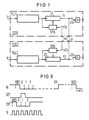
- the central clock supply consists of a first central clock generator CCG1 and a second central clock generator CCG2, whereby in normal operation of the central clock supply the first central clock generator CCG1 generates a first clock f 1 from the external reference clock f E via a first phase locked loop PLL1 and a first counter C1, which is connected through a switch s1a to the output of the clock supply and synchronizes the switching center as a public clock.
- the second central clock generator also forms a second phase control loop PLL2 and a second counter C2, a second clock f2 of the same frequency, which, however, only in the event of an emergency (in the event of failure of the first central clock generator or for routine test purposes) via a second switch s2a as the official clock to the Output of the central clock supply is switched through.
- switch s1a If switch s1a is closed, switch s2a is open and vice versa.
- a switch s1p and a switch S2p have the same relationship to one another. In normal operation of the central clock supply, switch s2p is closed and switch s1p is open, while when the normally active first central clock generator, the switch s2p is opened and the switch s1p is closed.
- a synchronization circuit SYN which, for example, registers every falling edge of the reference clock and resets a counter with the subsequent rising edge of a counting clock, as a result of which the clock generated by this counter is constantly synchronized with the reference clock.
- the supply of the synchronization with the reference clock occurs via a reference line L R.
- pulses occur on the reference line, e.g. in the event of a sudden failure of the reference clock or due to undesired overcouplings to the reference line, their falling edges also lead to synchronization and, in the special example according to FIG.
- the invention has for its object to ensure error-free synchronization of a clock to a reference clock.
- a retriggerable monostable multivibrator allows in a particularly simple manner to prevent unauthorized synchronization if the reference clock fails.
- a time window with respect to the clock is also determined in a particularly simple manner by a comparator.
- a further embodiment of the arrangement according to claim 5 is used for the appropriate circuit implementation of the requirement that synchronization may generally only take place if a certain edge of the reference clock is within a certain periodically recurring time range.
- a circuit arrangement SYN for synchronizing a clock f to a reference clock f R with the aid of a counter C consists of a comparator Vg, a device E, a second counter C2 and a retriggerable monostable multivibrator MF.
- the comparator Vg immediately receives the status of the counter C, which it compares with the values of its internal value set (0, 1, 2). Its output is zero if and only if the counter C is 0, 1 or 2. In this way, it generates with its output a window signal CEP which generates a time window ZF defined by the values 0, 1, 2 with respect to the clock f.
- a time window could also be implemented in a somewhat more complex manner with a synchronous counter in conjunction with a small logic.
- the size of the time window ZF depends on the extent to which the clock f normally drifts away from the reference clock in a period 1 / f without the synchronization circuit SYN according to the invention, i.e. how far the certain flanks of the two bars move against each other.
- the device E generates a synchronization pulse SI which, on the one hand, brings about the synchronization of the clock to the reference clock f R by reloading L of the counter C and, on the other hand, simultaneously reloading L of the second counter C2.
- the time of reloading is determined by the rising edge of a counter clock f c .
- the device E consists of an edge detector FD and combinatorial logic in the form of a switching network SN.
- the edge detector generates a pulse of a counter enable signal CET which has the period length of the counter clock f c from each falling edge of the reference clock with the next rising edge of the counter clock f C.
- the output of the switching network which supplies the synchronization pulse, is at logic 0 if and only if either the counter enable signal CET is at logic 1 and the window signal CEP is at logic 0, or a carry signal CI, which comes from the second counter, is at logic 1 and the window signal GEP is at logical 1.
- the synchronization pulse with the length of one period of the counting clock Except for the transmission signal CI, it is only generated when the negative edge of the reference clock f R falls in the time range that is identified by the counter readings 1023 (highest counter reading), 0, and 1 of counter C, that is, by one counter clock before the same time window ZF.
- the second counter C2 counts those pulses of the counter enable signal CET that lie outside the time window ZF defined by the window signal and, when it reaches its maximum level, generates the carry signal CI, which leads to the triggering of a synchronization pulse via the switching network SN.
- the pulse formed by the counter enable signal CET will generally be outside the time window and synchronization can therefore only take place after the second counter C2 has been counted up.
- the retriggerable monostable multivibrator MF has a time constant that is slightly larger than the period of the reference clock. This means that when the reference clock is applied, its output remains set to logic 1. If the reference clock fails, it returns to its stable state and causes after each period of the counter clock f c, a reset R of the second counter C2. This prevents the second counter from gradually reaching its maximum due to negative edges of individual pulses which nevertheless occur on the reference line L R for supplying the reference clock (for example by overcoupling) and could thereby erroneously cause synchronization.
- a microprocessor which is informed of the failure of the reference clock by monitoring.
- the microprocessor can then lock the synchronization circuit if the reference clock fails, for example with the aid of a signal SL, which it sets to zero for this purpose.
Landscapes
- Engineering & Computer Science (AREA)
- Computer Networks & Wireless Communication (AREA)
- Signal Processing (AREA)
- Synchronisation In Digital Transmission Systems (AREA)
- Synchronizing For Television (AREA)
- Stabilization Of Oscillater, Synchronisation, Frequency Synthesizers (AREA)
- Communication Control (AREA)
- Electric Clocks (AREA)
Applications Claiming Priority (2)
| Application Number | Priority Date | Filing Date | Title |
|---|---|---|---|
| DE3917712 | 1989-05-31 | ||
| DE3917712 | 1989-05-31 |
Publications (3)
| Publication Number | Publication Date |
|---|---|
| EP0400397A2 true EP0400397A2 (fr) | 1990-12-05 |
| EP0400397A3 EP0400397A3 (fr) | 1991-05-02 |
| EP0400397B1 EP0400397B1 (fr) | 1995-04-12 |
Family
ID=6381764
Family Applications (1)
| Application Number | Title | Priority Date | Filing Date |
|---|---|---|---|
| EP90109250A Expired - Lifetime EP0400397B1 (fr) | 1989-05-31 | 1990-05-16 | Procédé de synchronisation d'une horloge engendré à l'aide d'un compteur sur une horloge de référence |
Country Status (6)
| Country | Link |
|---|---|
| US (1) | US5052030A (fr) |
| EP (1) | EP0400397B1 (fr) |
| AT (1) | ATE121238T1 (fr) |
| DE (1) | DE59008876D1 (fr) |
| ES (1) | ES2070205T3 (fr) |
| GR (1) | GR3015779T3 (fr) |
Cited By (1)
| Publication number | Priority date | Publication date | Assignee | Title |
|---|---|---|---|---|
| DE4232037A1 (de) * | 1992-09-24 | 1994-03-31 | Siemens Ag | Schaltung mit zwei sich gegenseitig synchronisierenden spannungsgeregelten Oszillatoren |
Families Citing this family (9)
| Publication number | Priority date | Publication date | Assignee | Title |
|---|---|---|---|---|
| US5151591A (en) * | 1991-03-20 | 1992-09-29 | Honeywell Inc. | Asynchronous signal interrogation circuit for an detection apparatus |
| US5381542A (en) * | 1991-07-29 | 1995-01-10 | Unisys Corporation | System for switching between a plurality of clock sources upon detection of phase alignment thereof and disabling all other clock sources |
| US6308077B1 (en) * | 1992-10-02 | 2001-10-23 | Motorola, Inc. | Apparatus and method for providing synchronization of base-stations in a communication system |
| SE9300679L (sv) * | 1993-03-01 | 1994-09-02 | Ellemtel Utvecklings Ab | Bitsynkroniserare |
| JPH075949A (ja) * | 1993-06-18 | 1995-01-10 | Nec Corp | 2重化クロック切替えの方法と装置 |
| US5672988A (en) * | 1994-04-15 | 1997-09-30 | Linear Technology Corporation | High-speed switching regulator drive circuit |
| US6970045B1 (en) | 2003-06-25 | 2005-11-29 | Nel Frequency Controls, Inc. | Redundant clock module |
| JP7382980B2 (ja) | 2021-02-26 | 2023-11-17 | 株式会社安川電機 | コントローラ、機器制御システム、時刻同期方法、および時刻同期プログラム |
| JP7248044B2 (ja) | 2021-02-26 | 2023-03-29 | 株式会社安川電機 | コントローラ、機器制御システム、時刻同期方法、および時刻同期プログラム |
Family Cites Families (5)
| Publication number | Priority date | Publication date | Assignee | Title |
|---|---|---|---|---|
| IT7825268A0 (it) * | 1978-07-03 | 1978-07-03 | Sits Soc It Telecom Siemens | Disposizione circuitale per individuare l'elemento guasto in una pluralita' di oscillatori controllati in fase. |
| US4282493A (en) * | 1979-07-02 | 1981-08-04 | Motorola, Inc. | Redundant clock signal generating circuitry |
| FR2546691B1 (fr) * | 1983-05-27 | 1985-07-05 | Cit Alcatel | Base de temps asservie |
| US4583054A (en) * | 1984-11-13 | 1986-04-15 | Rca Corporation | Frequency time standard failure monitor |
| US4651103A (en) * | 1985-12-30 | 1987-03-17 | At&T Company | Phase adjustment system |
-
1990
- 1990-04-02 US US07/502,931 patent/US5052030A/en not_active Expired - Lifetime
- 1990-05-16 ES ES90109250T patent/ES2070205T3/es not_active Expired - Lifetime
- 1990-05-16 EP EP90109250A patent/EP0400397B1/fr not_active Expired - Lifetime
- 1990-05-16 AT AT90109250T patent/ATE121238T1/de not_active IP Right Cessation
- 1990-05-16 DE DE59008876T patent/DE59008876D1/de not_active Expired - Fee Related
-
1995
- 1995-04-13 GR GR950400884T patent/GR3015779T3/el unknown
Cited By (1)
| Publication number | Priority date | Publication date | Assignee | Title |
|---|---|---|---|---|
| DE4232037A1 (de) * | 1992-09-24 | 1994-03-31 | Siemens Ag | Schaltung mit zwei sich gegenseitig synchronisierenden spannungsgeregelten Oszillatoren |
Also Published As
| Publication number | Publication date |
|---|---|
| DE59008876D1 (de) | 1995-05-18 |
| US5052030A (en) | 1991-09-24 |
| ATE121238T1 (de) | 1995-04-15 |
| GR3015779T3 (en) | 1995-07-31 |
| ES2070205T3 (es) | 1995-06-01 |
| EP0400397B1 (fr) | 1995-04-12 |
| EP0400397A3 (fr) | 1991-05-02 |
Similar Documents
| Publication | Publication Date | Title |
|---|---|---|
| DE69124319T2 (de) | Bitsynchronisierung mittels elastisches Speichers | |
| DE4017494C2 (fr) | ||
| DE69702811T3 (de) | Stabilisation einer elektronischen Schaltung zur Regelung des mechanischen Gangwerks einer Zeitmessvorrichtung | |
| DE2144551A1 (de) | Synchronisierschaltung | |
| EP0400397B1 (fr) | Procédé de synchronisation d'une horloge engendré à l'aide d'un compteur sur une horloge de référence | |
| DE2725998A1 (de) | Vertikalsynchronisierschaltung | |
| DE3215783C2 (de) | Digitale Datenübertragungsanlage mit störungsfreiem Umschalten von regulären Kanälen auf einen Reservekanal | |
| EP0216113B1 (fr) | Synchronisateur | |
| DE3340553C2 (fr) | ||
| DE2622634A1 (de) | Anordnung zur ermittlung der phase des hilfstraegers in einem pal- signal | |
| DE2930586A1 (de) | Schaltungsanordnung zur synchronisierung einer untergeordneten einrichtung, insbesondere einer digitalen teilnehmerstation, durch eine uebergeordnete einrichtung, insbesondere eine digitale vermittlungsstelle eines pcm-fernmeldenetzes | |
| DE3888133T2 (de) | Datenmustersynchronisiereinrichtung. | |
| DE69210158T2 (de) | Verriegelungsdetektor eines digitalen Phasenregelkreises | |
| DE2808762C2 (fr) | ||
| EP0012185A1 (fr) | Circuit de test pour le fonctionnement synchrone de générateurs de cadence | |
| EP0100076B1 (fr) | Arrangement pour la génération de signaux d'horloge dans des installations de télécommunication, en particulier des centraux numériques temporels | |
| EP0429140B1 (fr) | Dispositif numérique de synchronisation | |
| EP0491084A1 (fr) | Dispositif pour produire des signaux synchrones pour synchroniser des blocs de télégrammes de données codées en code de blocs avec mots de correction et utilisation | |
| DE3715595C2 (fr) | ||
| DE3832330C2 (de) | Schaltungsanordnung zur Ableitung von horizontalfrequenten und veritikalfrequenten Impulsen | |
| DE3227849A1 (de) | Schaltungsanordnung zur takterzeugung in fernmeldeanlagen, insbesondere zeitmultiplex-digital-vermittlungsanlagen | |
| DE2933322A1 (de) | Schaltungsanordnung zum ableiten eines bittaktsignals aus einem digitalsignal | |
| DE3633024C2 (de) | Schaltungsanordnung für die Phasensynchronisierung zweier Taktimpulsfolgen | |
| DE2832589C2 (fr) | ||
| DE2351478B2 (de) | Verfahren zur Synchronisation des Zeitrahmens im Empfaenger eines Zeitmultiplex-UEbertragungssystems auf den Zeitrahmen des Senders |
Legal Events
| Date | Code | Title | Description |
|---|---|---|---|
| PUAI | Public reference made under article 153(3) epc to a published international application that has entered the european phase |
Free format text: ORIGINAL CODE: 0009012 |
|
| AK | Designated contracting states |
Kind code of ref document: A2 Designated state(s): AT BE CH DE ES FR GB GR IT LI NL SE |
|
| 17P | Request for examination filed |
Effective date: 19901205 |
|
| PUAL | Search report despatched |
Free format text: ORIGINAL CODE: 0009013 |
|
| AK | Designated contracting states |
Kind code of ref document: A3 Designated state(s): AT BE CH DE ES FR GB GR IT LI NL SE |
|
| 17Q | First examination report despatched |
Effective date: 19940310 |
|
| GRAA | (expected) grant |
Free format text: ORIGINAL CODE: 0009210 |
|
| AK | Designated contracting states |
Kind code of ref document: B1 Designated state(s): AT BE CH DE ES FR GB GR IT LI NL SE |
|
| REF | Corresponds to: |
Ref document number: 121238 Country of ref document: AT Date of ref document: 19950415 Kind code of ref document: T |
|
| REF | Corresponds to: |
Ref document number: 59008876 Country of ref document: DE Date of ref document: 19950518 |
|
| REG | Reference to a national code |
Ref country code: ES Ref legal event code: FG2A Ref document number: 2070205 Country of ref document: ES Kind code of ref document: T3 |
|
| ITF | It: translation for a ep patent filed | ||
| REG | Reference to a national code |
Ref country code: GR Ref legal event code: FG4A Free format text: 3015779 |
|
| GBT | Gb: translation of ep patent filed (gb section 77(6)(a)/1977) |
Effective date: 19950619 |
|
| ET | Fr: translation filed | ||
| PGFP | Annual fee paid to national office [announced via postgrant information from national office to epo] |
Ref country code: CH Payment date: 19950817 Year of fee payment: 6 |
|
| PLBE | No opposition filed within time limit |
Free format text: ORIGINAL CODE: 0009261 |
|
| STAA | Information on the status of an ep patent application or granted ep patent |
Free format text: STATUS: NO OPPOSITION FILED WITHIN TIME LIMIT |
|
| 26N | No opposition filed | ||
| PGFP | Annual fee paid to national office [announced via postgrant information from national office to epo] |
Ref country code: GB Payment date: 19960419 Year of fee payment: 7 |
|
| PGFP | Annual fee paid to national office [announced via postgrant information from national office to epo] |
Ref country code: AT Payment date: 19960426 Year of fee payment: 7 |
|
| PGFP | Annual fee paid to national office [announced via postgrant information from national office to epo] |
Ref country code: GR Payment date: 19960509 Year of fee payment: 7 |
|
| PGFP | Annual fee paid to national office [announced via postgrant information from national office to epo] |
Ref country code: ES Payment date: 19960510 Year of fee payment: 7 |
|
| PGFP | Annual fee paid to national office [announced via postgrant information from national office to epo] |
Ref country code: SE Payment date: 19960514 Year of fee payment: 7 |
|
| PGFP | Annual fee paid to national office [announced via postgrant information from national office to epo] |
Ref country code: BE Payment date: 19960515 Year of fee payment: 7 |
|
| PGFP | Annual fee paid to national office [announced via postgrant information from national office to epo] |
Ref country code: FR Payment date: 19960523 Year of fee payment: 7 |
|
| PG25 | Lapsed in a contracting state [announced via postgrant information from national office to epo] |
Ref country code: LI Effective date: 19960531 Ref country code: CH Effective date: 19960531 |
|
| PGFP | Annual fee paid to national office [announced via postgrant information from national office to epo] |
Ref country code: NL Payment date: 19960531 Year of fee payment: 7 |
|
| REG | Reference to a national code |
Ref country code: CH Ref legal event code: PL |
|
| PG25 | Lapsed in a contracting state [announced via postgrant information from national office to epo] |
Ref country code: GB Effective date: 19970516 Ref country code: AT Effective date: 19970516 |
|
| PG25 | Lapsed in a contracting state [announced via postgrant information from national office to epo] |
Ref country code: SE Effective date: 19970517 Ref country code: ES Free format text: LAPSE BECAUSE OF NON-PAYMENT OF DUE FEES Effective date: 19970517 |
|
| PG25 | Lapsed in a contracting state [announced via postgrant information from national office to epo] |
Ref country code: BE Effective date: 19970531 |
|
| BERE | Be: lapsed |
Owner name: SIEMENS A.G. Effective date: 19970531 |
|
| PG25 | Lapsed in a contracting state [announced via postgrant information from national office to epo] |
Ref country code: GR Free format text: THE PATENT HAS BEEN ANNULLED BY A DECISION OF A NATIONAL AUTHORITY Effective date: 19971130 |
|
| PG25 | Lapsed in a contracting state [announced via postgrant information from national office to epo] |
Ref country code: NL Effective date: 19971201 |
|
| REG | Reference to a national code |
Ref country code: GR Ref legal event code: MM2A Free format text: 3015779 |
|
| GBPC | Gb: european patent ceased through non-payment of renewal fee |
Effective date: 19970516 |
|
| PG25 | Lapsed in a contracting state [announced via postgrant information from national office to epo] |
Ref country code: FR Free format text: LAPSE BECAUSE OF NON-PAYMENT OF DUE FEES Effective date: 19980130 |
|
| EUG | Se: european patent has lapsed |
Ref document number: 90109250.2 |
|
| NLV4 | Nl: lapsed or anulled due to non-payment of the annual fee |
Effective date: 19971201 |
|
| REG | Reference to a national code |
Ref country code: FR Ref legal event code: ST |
|
| REG | Reference to a national code |
Ref country code: ES Ref legal event code: FD2A Effective date: 19990405 |
|
| PG25 | Lapsed in a contracting state [announced via postgrant information from national office to epo] |
Ref country code: IT Free format text: LAPSE BECAUSE OF NON-PAYMENT OF DUE FEES Effective date: 20050516 |
|
| PGFP | Annual fee paid to national office [announced via postgrant information from national office to epo] |
Ref country code: DE Payment date: 20050721 Year of fee payment: 16 |
|
| PG25 | Lapsed in a contracting state [announced via postgrant information from national office to epo] |
Ref country code: DE Free format text: LAPSE BECAUSE OF NON-PAYMENT OF DUE FEES Effective date: 20061201 |