EP0401577A1 - Metalloxyd-Halbleiteranordnung und Verfahren zur Herstellung - Google Patents
Metalloxyd-Halbleiteranordnung und Verfahren zur Herstellung Download PDFInfo
- Publication number
- EP0401577A1 EP0401577A1 EP90109511A EP90109511A EP0401577A1 EP 0401577 A1 EP0401577 A1 EP 0401577A1 EP 90109511 A EP90109511 A EP 90109511A EP 90109511 A EP90109511 A EP 90109511A EP 0401577 A1 EP0401577 A1 EP 0401577A1
- Authority
- EP
- European Patent Office
- Prior art keywords
- region
- single crystal
- insulator
- semiconductor substrate
- crystal semiconductor
- Prior art date
- Legal status (The legal status is an assumption and is not a legal conclusion. Google has not performed a legal analysis and makes no representation as to the accuracy of the status listed.)
- Granted
Links
Images


Classifications
-
- H—ELECTRICITY
- H10—SEMICONDUCTOR DEVICES; ELECTRIC SOLID-STATE DEVICES NOT OTHERWISE PROVIDED FOR
- H10D—INORGANIC ELECTRIC SEMICONDUCTOR DEVICES
- H10D30/00—Field-effect transistors [FET]
- H10D30/60—Insulated-gate field-effect transistors [IGFET]
- H10D30/67—Thin-film transistors [TFT]
- H10D30/674—Thin-film transistors [TFT] characterised by the active materials
- H10D30/6741—Group IV materials, e.g. germanium or silicon carbide
- H10D30/6743—Silicon
- H10D30/6744—Monocrystalline silicon
-
- H—ELECTRICITY
- H10—SEMICONDUCTOR DEVICES; ELECTRIC SOLID-STATE DEVICES NOT OTHERWISE PROVIDED FOR
- H10D—INORGANIC ELECTRIC SEMICONDUCTOR DEVICES
- H10D30/00—Field-effect transistors [FET]
- H10D30/01—Manufacture or treatment
- H10D30/021—Manufacture or treatment of FETs having insulated gates [IGFET]
- H10D30/031—Manufacture or treatment of FETs having insulated gates [IGFET] of thin-film transistors [TFT]
- H10D30/0321—Manufacture or treatment of FETs having insulated gates [IGFET] of thin-film transistors [TFT] comprising silicon, e.g. amorphous silicon or polysilicon
- H10D30/0323—Manufacture or treatment of FETs having insulated gates [IGFET] of thin-film transistors [TFT] comprising silicon, e.g. amorphous silicon or polysilicon comprising monocrystalline silicon
-
- H—ELECTRICITY
- H10—SEMICONDUCTOR DEVICES; ELECTRIC SOLID-STATE DEVICES NOT OTHERWISE PROVIDED FOR
- H10D—INORGANIC ELECTRIC SEMICONDUCTOR DEVICES
- H10D30/00—Field-effect transistors [FET]
- H10D30/60—Insulated-gate field-effect transistors [IGFET]
- H10D30/67—Thin-film transistors [TFT]
- H10D30/6704—Thin-film transistors [TFT] having supplementary regions or layers in the thin films or in the insulated bulk substrates for controlling properties of the device
- H10D30/6706—Thin-film transistors [TFT] having supplementary regions or layers in the thin films or in the insulated bulk substrates for controlling properties of the device for preventing leakage current
-
- H—ELECTRICITY
- H10—SEMICONDUCTOR DEVICES; ELECTRIC SOLID-STATE DEVICES NOT OTHERWISE PROVIDED FOR
- H10D—INORGANIC ELECTRIC SEMICONDUCTOR DEVICES
- H10D30/00—Field-effect transistors [FET]
- H10D30/60—Insulated-gate field-effect transistors [IGFET]
- H10D30/67—Thin-film transistors [TFT]
- H10D30/6704—Thin-film transistors [TFT] having supplementary regions or layers in the thin films or in the insulated bulk substrates for controlling properties of the device
- H10D30/6713—Thin-film transistors [TFT] having supplementary regions or layers in the thin films or in the insulated bulk substrates for controlling properties of the device characterised by the properties of the source or drain regions, e.g. compositions or sectional shapes
-
- H—ELECTRICITY
- H10—SEMICONDUCTOR DEVICES; ELECTRIC SOLID-STATE DEVICES NOT OTHERWISE PROVIDED FOR
- H10D—INORGANIC ELECTRIC SEMICONDUCTOR DEVICES
- H10D30/00—Field-effect transistors [FET]
- H10D30/60—Insulated-gate field-effect transistors [IGFET]
- H10D30/67—Thin-film transistors [TFT]
- H10D30/674—Thin-film transistors [TFT] characterised by the active materials
- H10D30/6755—Oxide semiconductors, e.g. zinc oxide, copper aluminium oxide or cadmium stannate
-
- H—ELECTRICITY
- H10—SEMICONDUCTOR DEVICES; ELECTRIC SOLID-STATE DEVICES NOT OTHERWISE PROVIDED FOR
- H10D—INORGANIC ELECTRIC SEMICONDUCTOR DEVICES
- H10D30/00—Field-effect transistors [FET]
- H10D30/60—Insulated-gate field-effect transistors [IGFET]
- H10D30/67—Thin-film transistors [TFT]
- H10D30/6757—Thin-film transistors [TFT] characterised by the structure of the channel, e.g. transverse or longitudinal shape or doping profile
Definitions
- the MOS integrated circuits are required to have a breakdown voltage which is about two times as large as the supply voltage in consideration of the noise in the supply voltage and the substrate biasing.
- the breakdown voltage is usually set to 5 volts, the breakdown voltage of 10 volts or less is apparently insufficient.
- this prior art MOS transistor can eliminate the back channel effect by the isolated doped region interrupting the formation of the inversion layer extending between the source and drain regions along the boundary to the underlying silicon oxide substrate, it has a problem in that a neutral region is formed in the channel region because of the relatively large thickness of the channel layer (about 0.5 ⁇ m) which prevents the depletion region formed during the operation of the transistor from extending to and reaching the boundary to the underlying silicon oxide layer. When this occurs, there is a possibility that holes, which may be formed during the operation of the transistor as a result of impact ionization, are accumulated in the neutral region.
- the silicon single crystal layer is biased with respect to the source region and there appears a parasitic bipolar action in the parasitic bipolar transistor formed by the source region, drain region and the channel region intervening therebwtween.
- a parasitic bipolar action occurs, a large amount of carriers are caused to flow between the source and drain regions and the breakdown voltage between the source and drain regions is significantly decreased.
- the MOS transistor of this reference is also disadvantageous from the viewpoint of forming a parasitic capacitance under the overhanging drain region which reduces the operational speed of the transistor.
- such a MOS transistor having the offset gate structure occupies a large area and is disadvantageous from the view point of increasing the integration density of the integrated circuit.
- the resistance caused by the overhanging drain region provides an effect of reducing the operational speed.
- an SOI semiconductor body including a silicon oxide substrate 10 and a p-type single crystal silicon layer 11 is subjected to a thermal oxidation process wherein a silicon oxide film 12 having a thickness of about 200 ⁇ is formed on the silicon layer 11.
- the single crystal silicon layer 11 are divided into a number of portions which are separated from each other by a silicon oxide isolation region 19.
- the SOI semiconductor body may be formed by binding a pair of semiconductor wafers each having an oxidized surface such that the oxidized surfaces are contacted each other.
- the SOI semiconductor body may be formed by the so-called SIMOX process wherein oxygen ions are selectively implanted to a semiconductor wafer in correspondence to the depth of the silicon substrate.
- the p-type silicon layer 11 has a thickness of about 0.1 ⁇ m and a specific resistance of about 10 ⁇ .cm.
- the SOI semiconductor body is used in a state that it is supported by a silicon wafer.
- the silicon oxide film 12 is formed on the p-type silicon layer 11 in order to prevent the contamination of the silicon layer 11 from the photoresist applied in the subsequent process and at the same time for preventing the occurrence of the channeling in response to the ion implantation. Further, the silicon oxide film 12 acts to remove the impurities from the silicon layer 11 and protects the surface of the silicon layer 11.
- a photoresist 13 is applied on the top surface of the silicon oxide film 12 and a part thereof having a size D is removed photolithographically as a window in correspondence to the gate electrode to be formed in the later process.
- the size D is chosen to be 0.5 ⁇ m as will be described.
- an ion implantation of boron (B+) is performed under an acceleration voltage of 30 - 40 keV with a dose of 3 X 1013 cm ⁇ 2.
- the boron ions are implanted into the silicon layer 11 in correspondence to the removed part of the photoresist.
- Most of the boron ions thus implanted reach the depth close to the boundary between the silicon layer 11 and the silicon oxide layer 10 underneath as shown in FIG.4C.
- the photoresist 13 is removed and the silicon oxide film 12 is removed also subsequently.
- the substrate thus obtained is subjected to a thermal oxidation under hydrochloride vapor at a temperature between 900 - 950°C.
- a gate insulation film 15 is formed on the surface of the silicon layer 11.
- the implanted boron ions are activated and a p+-type region 16 of increased impurity concentration level is formed as illustrated in FIG.4D.
- the dotted boundary of the region 16 shows the concentration profile of boron which is reduced by a factor of about two orders of magnitude (102) with respect to the maximum concentration of boron in the region 16.
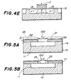
- a gate electrode 17 of polysilicon is deposited on the gate insulator film 15 by a CVD process and patterned subsequently such that the gate electrode 17 remains above the region 16 for a gate length L of 0.8 ⁇ m as shown in FIG.4E.
- This gate electrode 17 may be a lamination of polysilicon and silicide.
- the alignment between the patterned gate electrode 17 and the region 16 located below the gate electrode 17 can be achieved with an alignment accuracy within about 0.03 ⁇ m using the same stepper.
- the size D of the window formed in the photoresist 13 is chosen such that the size D is smaller than the gate length L by 0.2 - 0.3 ⁇ m or more. As already described, the size D is set to 0.5 ⁇ m and the gate length L is set to 0.8 ⁇ m in the foregoing embodiment. By choosing the size D of the window as such, the region 16 remains invariably smaller than the gate electrode 17.
- a silicon oxide film 22 is deposited on the layer 21 by a low temperature CVD process at a temperature of 400°C for a thickness of 200 ⁇ , and a part of the polysilicon layer 21 and the silicon oxide film 22 corresponding to the gate of the MOS transistor to be formed is removed by etching for a size L′ to form an window 100.
- This size L′ corresponds to the gate length of the desired MOS transistor.
- FIG.5D shows the semiconductor device after the foregoing processes.
- the region 25 for eliminating the back channel effect is separated from the source and drain regions 26.
- the p+-type region 25 does not form the p-n junction with the source or drain region 26 directly, and thereby the problem of unwanted decrease of the drain breakdown voltage is successfully eliminated.
Landscapes
- Thin Film Transistor (AREA)
Applications Claiming Priority (2)
| Application Number | Priority Date | Filing Date | Title |
|---|---|---|---|
| JP127501/89 | 1989-05-20 | ||
| JP1127501A JP2782781B2 (ja) | 1989-05-20 | 1989-05-20 | 半導体装置の製造方法 |
Publications (2)
| Publication Number | Publication Date |
|---|---|
| EP0401577A1 true EP0401577A1 (de) | 1990-12-12 |
| EP0401577B1 EP0401577B1 (de) | 1996-12-27 |
Family
ID=14961535
Family Applications (1)
| Application Number | Title | Priority Date | Filing Date |
|---|---|---|---|
| EP90109511A Expired - Lifetime EP0401577B1 (de) | 1989-05-20 | 1990-05-18 | Metalloxyd-Halbleiteranordnung und Verfahren zur Herstellung |
Country Status (4)
| Country | Link |
|---|---|
| EP (1) | EP0401577B1 (de) |
| JP (1) | JP2782781B2 (de) |
| KR (1) | KR930008023B1 (de) |
| DE (1) | DE69029485T2 (de) |
Cited By (3)
| Publication number | Priority date | Publication date | Assignee | Title |
|---|---|---|---|---|
| EP0704910A3 (de) * | 1994-09-30 | 1997-09-03 | Sgs Thomson Microelectronics | Dünnfilmschichttransistor und dessen Herstellungsverfahren |
| WO2001050515A1 (en) * | 2000-01-07 | 2001-07-12 | Seiko Epson Corporation | Thin-film transistor |
| WO2001050516A1 (en) * | 2000-01-07 | 2001-07-12 | Seiko Epson Corporation | Method of manufacturing a thin-film transistor |
Families Citing this family (2)
| Publication number | Priority date | Publication date | Assignee | Title |
|---|---|---|---|---|
| JP4987259B2 (ja) * | 2005-07-12 | 2012-07-25 | セイコーインスツル株式会社 | 半導体装置の製造方法 |
| JP2007027201A (ja) * | 2005-07-12 | 2007-02-01 | Seiko Instruments Inc | 半導体装置の製造方法 |
Citations (3)
| Publication number | Priority date | Publication date | Assignee | Title |
|---|---|---|---|---|
| DE2641302A1 (de) * | 1976-09-14 | 1978-03-16 | Siemens Ag | N-kanal mis-fet in esfi-technik |
| US4106045A (en) * | 1975-05-20 | 1978-08-08 | The President Of The Agency Of Industrial Science And Technology | Field effect transistors |
| US4675981A (en) * | 1984-11-26 | 1987-06-30 | Kabushiki Kaisha Toshiba | Method of making implanted device regions in a semiconductor using a master mask member |
Family Cites Families (2)
| Publication number | Priority date | Publication date | Assignee | Title |
|---|---|---|---|---|
| JPS58139471A (ja) * | 1982-02-15 | 1983-08-18 | Fujitsu Ltd | Mis電界効果トランジスタ |
| JPS63114266A (ja) * | 1986-10-31 | 1988-05-19 | Fujitsu Ltd | 半導体装置の製造方法 |
-
1989
- 1989-05-20 JP JP1127501A patent/JP2782781B2/ja not_active Expired - Lifetime
-
1990
- 1990-05-18 DE DE69029485T patent/DE69029485T2/de not_active Expired - Fee Related
- 1990-05-18 EP EP90109511A patent/EP0401577B1/de not_active Expired - Lifetime
- 1990-05-21 KR KR9007273A patent/KR930008023B1/ko not_active Expired - Fee Related
Patent Citations (3)
| Publication number | Priority date | Publication date | Assignee | Title |
|---|---|---|---|---|
| US4106045A (en) * | 1975-05-20 | 1978-08-08 | The President Of The Agency Of Industrial Science And Technology | Field effect transistors |
| DE2641302A1 (de) * | 1976-09-14 | 1978-03-16 | Siemens Ag | N-kanal mis-fet in esfi-technik |
| US4675981A (en) * | 1984-11-26 | 1987-06-30 | Kabushiki Kaisha Toshiba | Method of making implanted device regions in a semiconductor using a master mask member |
Non-Patent Citations (1)
| Title |
|---|
| PATENT ABSTRACTS OF JAPAN vol. 5, no. 11 (E-42)(683) 23 January 1981, & JP-A-55 140270 (KOGYO GIJUTSUIN) 01 November 1980, * |
Cited By (7)
| Publication number | Priority date | Publication date | Assignee | Title |
|---|---|---|---|---|
| EP0704910A3 (de) * | 1994-09-30 | 1997-09-03 | Sgs Thomson Microelectronics | Dünnfilmschichttransistor und dessen Herstellungsverfahren |
| WO2001050515A1 (en) * | 2000-01-07 | 2001-07-12 | Seiko Epson Corporation | Thin-film transistor |
| WO2001050516A1 (en) * | 2000-01-07 | 2001-07-12 | Seiko Epson Corporation | Method of manufacturing a thin-film transistor |
| US6621101B2 (en) | 2000-01-07 | 2003-09-16 | Seiko Epson Corporation | Thin-film transistor |
| GB2358079B (en) * | 2000-01-07 | 2004-02-18 | Seiko Epson Corp | Thin-film transistor |
| US6727123B2 (en) | 2000-01-07 | 2004-04-27 | Seiko Epson Corporation | Method for manufacturing a thin-film transistor comprising a recombination center |
| GB2358080B (en) * | 2000-01-07 | 2004-06-02 | Seiko Epson Corp | Method of manufacturing a thin-film transistor |
Also Published As
| Publication number | Publication date |
|---|---|
| KR900019128A (ko) | 1990-12-24 |
| JPH02306665A (ja) | 1990-12-20 |
| KR930008023B1 (en) | 1993-08-25 |
| DE69029485D1 (de) | 1997-02-06 |
| JP2782781B2 (ja) | 1998-08-06 |
| EP0401577B1 (de) | 1996-12-27 |
| DE69029485T2 (de) | 1997-04-10 |
Similar Documents
| Publication | Publication Date | Title |
|---|---|---|
| US5547885A (en) | Method of making asymmetric LDD transistor | |
| US6316302B1 (en) | Isotropically etching sidewall spacers to be used for both an NMOS source/drain implant and a PMOS LDD implant | |
| US6518623B1 (en) | Semiconductor device having a buried-channel MOS structure | |
| US4637124A (en) | Process for fabricating semiconductor integrated circuit device | |
| EP0370809A2 (de) | Dünnfilm-SOI-MOSFET und Verfahren zur Herstellung | |
| JP2707977B2 (ja) | Mos型半導体装置およびその製造方法 | |
| EP0248292A2 (de) | Halbleiteranordnung mit hoher Durchbruchsspannung | |
| US5804856A (en) | Depleted sidewall-poly LDD transistor | |
| US5238857A (en) | Method of fabricating a metal-oxide-semiconductor device having a semiconductor on insulator (SOI) structure | |
| JPH07122657A (ja) | 半導体メモリとその製法 | |
| EP0401577B1 (de) | Metalloxyd-Halbleiteranordnung und Verfahren zur Herstellung | |
| US7148096B2 (en) | Method of manufacturing a semiconductor device having a gate electrode containing polycrystalline silicon-germanium | |
| JPH0685262A (ja) | 電界効果トランジスタおよびその製造方法 | |
| US5521416A (en) | Semiconductor device having gate electrode and impurity diffusion layer different in conductivity type and method of manufacturing the same | |
| JPH07153952A (ja) | 半導体装置及びその製造方法 | |
| JP3106757B2 (ja) | Mos電界効果半導体装置の製造方法 | |
| JP2729422B2 (ja) | 半導体装置 | |
| JPH098135A (ja) | 半導体装置の製造方法 | |
| JPH09223797A (ja) | 半導体装置の製造方法 | |
| JP3257317B2 (ja) | 半導体装置の製造方法 | |
| JP2519541B2 (ja) | 半導体装置 | |
| JPH09181313A (ja) | Mosfetの製造方法 | |
| JPS6129176A (ja) | 半導体装置の製造方法 | |
| JPH06232394A (ja) | 半導体装置の製造方法 | |
| KR930006853B1 (ko) | 소오스/드레인 자기정합 방식의 반도체 장치의 제조방법 |
Legal Events
| Date | Code | Title | Description |
|---|---|---|---|
| PUAI | Public reference made under article 153(3) epc to a published international application that has entered the european phase |
Free format text: ORIGINAL CODE: 0009012 |
|
| AK | Designated contracting states |
Kind code of ref document: A1 Designated state(s): DE FR GB |
|
| 17P | Request for examination filed |
Effective date: 19901228 |
|
| 17Q | First examination report despatched |
Effective date: 19930201 |
|
| GRAG | Despatch of communication of intention to grant |
Free format text: ORIGINAL CODE: EPIDOS AGRA |
|
| GRAH | Despatch of communication of intention to grant a patent |
Free format text: ORIGINAL CODE: EPIDOS IGRA |
|
| GRAH | Despatch of communication of intention to grant a patent |
Free format text: ORIGINAL CODE: EPIDOS IGRA |
|
| GRAA | (expected) grant |
Free format text: ORIGINAL CODE: 0009210 |
|
| AK | Designated contracting states |
Kind code of ref document: B1 Designated state(s): DE FR GB |
|
| REF | Corresponds to: |
Ref document number: 69029485 Country of ref document: DE Date of ref document: 19970206 |
|
| ET | Fr: translation filed | ||
| PLBE | No opposition filed within time limit |
Free format text: ORIGINAL CODE: 0009261 |
|
| STAA | Information on the status of an ep patent application or granted ep patent |
Free format text: STATUS: NO OPPOSITION FILED WITHIN TIME LIMIT |
|
| 26N | No opposition filed | ||
| REG | Reference to a national code |
Ref country code: GB Ref legal event code: IF02 |
|
| PGFP | Annual fee paid to national office [announced via postgrant information from national office to epo] |
Ref country code: DE Payment date: 20060511 Year of fee payment: 17 |
|
| PGFP | Annual fee paid to national office [announced via postgrant information from national office to epo] |
Ref country code: FR Payment date: 20060515 Year of fee payment: 17 |
|
| PGFP | Annual fee paid to national office [announced via postgrant information from national office to epo] |
Ref country code: GB Payment date: 20060517 Year of fee payment: 17 |
|
| GBPC | Gb: european patent ceased through non-payment of renewal fee |
Effective date: 20070518 |
|
| REG | Reference to a national code |
Ref country code: FR Ref legal event code: ST Effective date: 20080131 |
|
| PG25 | Lapsed in a contracting state [announced via postgrant information from national office to epo] |
Ref country code: DE Free format text: LAPSE BECAUSE OF NON-PAYMENT OF DUE FEES Effective date: 20071201 |
|
| PG25 | Lapsed in a contracting state [announced via postgrant information from national office to epo] |
Ref country code: GB Free format text: LAPSE BECAUSE OF NON-PAYMENT OF DUE FEES Effective date: 20070518 |
|
| PG25 | Lapsed in a contracting state [announced via postgrant information from national office to epo] |
Ref country code: FR Free format text: LAPSE BECAUSE OF NON-PAYMENT OF DUE FEES Effective date: 20070531 |