EP0401786A2 - Méthode de fabrication d'un transistor bipolaire latéral - Google Patents
Méthode de fabrication d'un transistor bipolaire latéral Download PDFInfo
- Publication number
- EP0401786A2 EP0401786A2 EP90110698A EP90110698A EP0401786A2 EP 0401786 A2 EP0401786 A2 EP 0401786A2 EP 90110698 A EP90110698 A EP 90110698A EP 90110698 A EP90110698 A EP 90110698A EP 0401786 A2 EP0401786 A2 EP 0401786A2
- Authority
- EP
- European Patent Office
- Prior art keywords
- impurity
- diffusion layer
- layer
- impurities
- conductivity type
- Prior art date
- Legal status (The legal status is an assumption and is not a legal conclusion. Google has not performed a legal analysis and makes no representation as to the accuracy of the status listed.)
- Granted
Links
Images


Classifications
-
- H—ELECTRICITY
- H10—SEMICONDUCTOR DEVICES; ELECTRIC SOLID-STATE DEVICES NOT OTHERWISE PROVIDED FOR
- H10D—INORGANIC ELECTRIC SEMICONDUCTOR DEVICES
- H10D62/00—Semiconductor bodies, or regions thereof, of devices having potential barriers
- H10D62/10—Shapes, relative sizes or dispositions of the regions of the semiconductor bodies; Shapes of the semiconductor bodies
- H10D62/17—Semiconductor regions connected to electrodes not carrying current to be rectified, amplified or switched, e.g. channel regions
- H10D62/177—Base regions of bipolar transistors, e.g. BJTs or IGBTs
- H10D62/184—Base regions of bipolar transistors, e.g. BJTs or IGBTs of lateral BJTs
-
- H—ELECTRICITY
- H10—SEMICONDUCTOR DEVICES; ELECTRIC SOLID-STATE DEVICES NOT OTHERWISE PROVIDED FOR
- H10D—INORGANIC ELECTRIC SEMICONDUCTOR DEVICES
- H10D10/00—Bipolar junction transistors [BJT]
- H10D10/01—Manufacture or treatment
- H10D10/051—Manufacture or treatment of vertical BJTs
-
- H—ELECTRICITY
- H10—SEMICONDUCTOR DEVICES; ELECTRIC SOLID-STATE DEVICES NOT OTHERWISE PROVIDED FOR
- H10D—INORGANIC ELECTRIC SEMICONDUCTOR DEVICES
- H10D10/00—Bipolar junction transistors [BJT]
- H10D10/60—Lateral BJTs
-
- Y—GENERAL TAGGING OF NEW TECHNOLOGICAL DEVELOPMENTS; GENERAL TAGGING OF CROSS-SECTIONAL TECHNOLOGIES SPANNING OVER SEVERAL SECTIONS OF THE IPC; TECHNICAL SUBJECTS COVERED BY FORMER USPC CROSS-REFERENCE ART COLLECTIONS [XRACs] AND DIGESTS
- Y10—TECHNICAL SUBJECTS COVERED BY FORMER USPC
- Y10S—TECHNICAL SUBJECTS COVERED BY FORMER USPC CROSS-REFERENCE ART COLLECTIONS [XRACs] AND DIGESTS
- Y10S148/00—Metal treatment
- Y10S148/01—Bipolar transistors-ion implantation
Definitions
- the present invention relates to a bipolar transistor and its manufacturing method.
- a lateral-structure pnp bipolar transistor is widely used in the art of manufacturing bipolar transistor integrated circuits, since it can be made simultaneously by use of the same manufacturing process as an npn bipolar transistor.
- the current amplification factor and frequency characteristic of the lateral-structure pnp bipolar transistor are not very satisfactory.
- a large number of small-sized, high-speed operation self-alignment type npn bipolar transistors have come to be manufactured, wherein the layer for leading out the base electrode is formed of polysilicon.
- reference numeral 401 denotes a p-type semiconductor substrate
- 402 denotes a high-concentration n+-type region
- 403 denotes a high-concentration p+-type channel cut region
- 404 denotes an n-type epitaxial layer
- 405 and 406 denote high-concentration p+-type regions, respectively
- 407 denotes an element-isolation region
- 408, 409 and 410 denote polysilicon layers, respectively
- 413, 414 and 415 denote electrodes formed of aluminum, respectively.
- the n-type regions 402 and 404 jointly constitute a base region
- the high-concentration p+-type region indicated with 405 constitutes a collector region
- the high-concentration p+-type region indicated with 406 constitutes an emitter region.
- the polysilicon layer indicated with 408 serves as a collector-leading layer for leading out the collector
- the polysilicon layer indicated with 409 serves as a base-leading layer for leading out the base
- the polysilicon layer indicated with 410 serves as an emitter-leading layer for leading out the emitter.
- the aluminum electrode indicated with 413 serves as a collector electrode
- the aluminum electrode indicated with 414 serves as an emitter electrode
- the aluminum electrode indicated with 415 serves as a base electrode.
- the high-concentration p+-type collector region 405 is formed by diffusing impurities from the polysilicon layer 408 (i.e., the collector-leading layer).
- the high-concentration p+-type emitter region 406 is formed by diffusing impurities from the polysilicon layer 410 (i.e., the emitter-leading layer).
- the base width is determined almost exclusively by the image resolution limit W of the lithography technique, i.e., the minimum design rule.
- the base width of a self-alignment type lateral-structure bipolar transistor can be smaller than that of a lateral-structure bipolar transistor which is not of a self-alignment type, so that the frequency characteristics of the former can be more improved than those of the latter. Under the circumstances, it may be thought to diffuse a large amount of impurities from the polysilicon layers 408 and 410 in the lateral direction, so as to reduce the base width further.
- the base width can be reduced only in the surface regions of the substrate; it remains almost unchanged in the regions which are deep from the surface of the substrate. This is because impurities diffuse radially and do not diffuse in the lateral direction alone. Thus, even if impurities are diffused in large quantities, the base width cannot be greatly reduced, and the frequency characteristics cannot be improved, as intended. In summary, it is safe to say that in actual devices, the image resolution limit W of the lithography technique exclusively determines the base width. Since the image resolution cannot be easily improved by use of the presently-available technology, the base width has to be reduced by using some other method.
- both the collector region 405 and the emitter region 406 become deeper as a result of the impurity diffusion. If they are deepened, the emitter junction which opposes the collector junction will increase in size, resulting in improvement of the current amplification factor. However, the increase in the size of the emitter junction prevents the fabrication of a small-sized element.
- the base width is dependent largely on the image resolution limit W of the lithography technique. For this reason, it is impossible to obtain a lateral-structure pnp bipolar transistor which has improved frequency characteristics and is suitable for the reduction of the size of an element.
- the present invention has been developed in consideration of the above circumstances, and an object of the invention is to provide a bipolar transistor which can be manufactured simultanenously by use of the same manufacturing process as npn bipolar transistors, has a reduced base width and is therefore improved in frequency characteristics, has a large-sized emitter junction opposing the collector junction and is therefore improved in current amplification factor, and is suitable for reducing the size of an element.
- Another object of the invention is to provide a method for manufacturing such a bipolar transistor.
- the present invention provides a bipolar transistor which comprises: a semiconductor substrate; first and second polycrystalline semiconductor layers formed on the semiconductor substrate, the first and second layers being separated from each other and used as an emitter-leading electrode and a collector-leading electrode, respectively; a third polycrystalline semiconductor layer formed on the semiconductor substrate and located between the first and second polycrystalline semiconductor layers, with an insulation film interposed; a first impurity-diffusion layer, of a first conductivity type, which is formed in the semiconductor substrate and is in contact with the first polycrystalline semiconductor layer; a second impurity-diffusion layer, of a second conductivity type, which is formed in the semiconductor substrate and is in contact with the first impurity-diffusion layer; a third impurity-diffusion layer, of the second conductivity type, which is formed in the semiconductor device and is in contact with both the third polycrystalline semiconductor layer and the second impurity-diffusion layer; a fourth impurity-diffusion layer, of the first
- the present invention provides a bipolar transistor-manufacturing method which comprises the steps of: forming a first insulation film on a semiconductor substrate; exposing a predetermined surface portion of the semiconductor substrate by selectively removing the first insulation film; forming a first crystalline semiconductor layer on the resultant semiconductor structure; forming a first photoresist film having a predetermined pattern on the first polycrystalline semiconductor layer; ion-implanting first impurities, which are of a first conductivity type, into the first polycrystalline semiconductor layer, using the first photoresist film as a mask; removing the first photoresist film; ion-implanting second impurities, which are of a second conductivity type and have a larger diffusion coefficient than that of the first impurities, into the first crystalline semiconductor layer through the entire surface thereof; forming a second insulation film on the first polycrystalline semiconductor layer; forming a second photoresist film having a predetermined pattern on the second insulation film; forming an opening to expose
- the base region i.e., the third impurity-diffusion layer in the case of the bipolar transistor; the fifth impurity-diffusion layer in the case of the method
- the polysilicon layer i.e., the third polycrystalline semiconductor layer in the case of the bipolar transistor; the fourth polycrystalline semiconductor in the case of the method.
- the base width can be considerably reduced without being restricted by the image resolution limit of the lithography technique. Therefore, frequency characteristics, particularly high-frequency characteristics, can be satisfactorily improved.
- the size of an element can be reduced.
- the collector region is located under the base region, and the emitter region is located above the base region.
- the impurity concentration profile of the bipolar transistor is similar to that of a vertical-structure bipolar transistor, so that the emitter junction opposing the collector junction can be increased in size. Accordingly, the current amplification factor can be also improved.
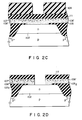
- a bipolar transistor according to one embodiment of the present invention and a method for manufacturing the bipolar transistor will now be described, with reference to Figs. 2A to 2J.
- Figs. 2A to 2J are sectional views illustrating the process in which a self-alignment type pnp bipolar transistor of the embodiment is manufactured.
- a semiconductor substrate 101 which is of e.g. a p type, is prepared, and an n-type epitaxial layer 102 having a thickness of 1 to 2 ⁇ m is formed on the semiconductor substrate 102 by vapor-phase growth. Thereafter, the resultant semiconductor structure is selectively oxidized in the LOCOS process, to thereby form an element-isolation region 104. Before this selective oxidization, p-type impurities, such as boron (B), are ion-implanted into a portion in which the element-isolation region 104 is to be formed.
- p-type impurities such as boron (B)
- the implanted ions are diffused by heat, with the result that a high-concentration p+-type channel cut region 103 is formed under the element-isolation region 104.
- the element isolation process available in the present invention is not limited to this. For example, a pn junction or an embedded layer may be formed for element separation.
- an oxide film 104′ is formed on the entire surface of the semiconductor structure by a thermal oxidization process. This oxide film 104′ is removed from the region in which an element is to be formed, to thereby expose that portion of the n-type epitaxial layer 102 on which the element is to be formed.
- a polysilicon layer 105 is grown on the entire surface of the semiconductor structure by CVD, for example, until the layer 105 has a thickness in the range of 2,000 to 4,000 ⁇ . Then, the entire surface of the polysilicon layer 105 is coated with photoresist. A photoresist film 106, thus obtained, is patterned into a predetermined shape by photo etching. By use of the patterned photoresist film 106 as a mask, n-type impurities 107, such as phosphor (P), which have a comparatively large diffusion coefficient, are ion-implanted into the polysilicon layer 105, with a dose of 1 ⁇ 1015 cm ⁇ 2.
- Reference numeral 107′ in Fig. 2A denotes ions of the n-type impurities implanted into the polysilicon layer 105.
- p-type impurities such as boron (B)
- B boron
- Reference numeral 108′ in Fig. 2B denotes ions of the p-type impurities implanted into the polysilicon layer 105.
- the polysilicon layer 105 is made to have two regions 109 and 110.
- Region 109 contains both n-type impurities 107′ (e.g., P) and p-type impurities 108′ (e.g., B), while region 110 contains only p-type impurities 108′.
- the semiconductor structure may be annealed, to such an extent that the ions 107′ of the n-type impurities do not diffuse from the polysilicon layer 105 into that portion of the n-type epitaxial layer 102 at which a collector electrode-leading region (to be mentioned later) is to be formed.
- an oxide film 111 is grown on the semiconductor structure by CVD, for example, until the oxide film 111 has a thickness in the range of 3,000 to 5,000 ⁇ . Then, a photoresist film 109 having a predetermined pattern is formed on the oxide film 111.
- the oxide film 111 and the polysilicon layer 105 are selectively etched out by photo etching and reactive ion etching, by use of the photoresist film 109 as a mask. By this selective etching, an opening extending to the epitaxial layer 102 is formed.
- an oxide film 112 is grown on the semiconductor structure by CVD, for example, until the oxide film 112 has a thickness in the range of 2,000 to 3,000 ⁇ .
- the oxide film 112 is selectively removed by reactive ion etching, such that it remains only on the side walls of the opening.
- an oxide film 113 is formed on the exposed surface portion of the epitaxial layer 102 by a thermal oxidization process, for example. Then, the semiconductor structure is annealed to a predetermined extent. By this annealing, ions 107′ of the n-type impurities (e.g., P) and ions 108′ of the p-type impurities (e.g., B) are diffused from the polysilicon layer 1051 into the n-type epitaxial layer 102. Further, ions 108 of the p-type impurities (e.g., B) are diffused from the polysilicon layer 1052 into the n-type epitaxial layer 102.
- n-type impurities e.g., P
- ions 108′ of the p-type impurities e.g., B
- a high-concentration p++-type emitter region 115 As a result, a high-concentration p++-type emitter region 115, a high-concentration n+-type region 116 (which serves as an internal base region), and a high-concentration p++-type collector electrode-leading region 114 are formed. Since, as mentioned above, the n-type impurities (e.g., P) and the p-type impurities (e.g., B) have different diffusion coefficients, the p++-type region 115 and the n+-type region 116 can be formed simultaneously by performing the heat treatment only once.
- the n-type impurities e.g., P
- the p-type impurities e.g., B
- p-type impurities such as boron (B)
- B boron
- the oxide film 113 inside the opening is removed by etching.
- a polysilicon layer 118 containing n-type impurities, such as arsenic (As) is grown on the semiconductor structure by CVD, until the polysilicon layer 118 has a thickness in the range of 1,000 to 3,000 ⁇ .
- n-type impurities thermally diffused from the polysilicon layer 118, a high-concentration n++-type region 119 serving as an external base region is formed.
- the polysilicon layer 118 is patterned into a predetermined shape by photo etching, to thereby form a base electrode-leading layer 118.
- an oxide film 120 is formed on the semiconductor structure by a thermal oxidization process, for example.
- three contact holes are formed in the oxide films 111 and 120 by photo etching, for example, such that one of the contact holes is located at a predetermined position on the polysilicon layer 118 and the others are located at respective predetermined positions on the polysilicon layer 105.
- an aluminum layer is formed on the semiconductor structure by sputtering. This aluminum layer is patterned into a predetermined shape, to thereby form a collection electrode 121, a base electrode 122 and an emitter electrode 123. In this manner, the bipolar transistor according to one embodiment of the present invention is manufactured.
- the base width is determined not by the image resolution limit of the lithography technique, as in the prior art, but by the impurity diffusion from the polysilicon layer 118. Therefore, the self-alignment type lateral-structure pnp bipolar transistor of the present invention and the manufacturing method thereof permit the base width to be as small as possible, resulting in improvement of frequency characteristics. In addition, they are suitable for obtaining a small-sized element.
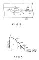
- Fig. 3 is an enlarged view of the intrinsic transistor region of a self-alignment type lateral-structure pnp bipolar transistor obtained in accordance with the present invention.
- the reference numerals in Fig. 3 correspond to those used in Fig. 2J.
- Fig. 4 is a graph showing the impurity concentrations of the diffusion regions viewed in the plane taken along line A-A′ in Fig. 3.
- the intrinsic transistor region extends along the section taken on line A-A′.
- the intrinsic transistor region does not extend in the horizontal direction, but extends slantwise. Due to this construction, the emitter junction opposing the collection junction is large, in comparison with the case where the intrinsic transistor region extends in a completely horizontal direction. As a result, the current amplification factor can be satisfactory.
- reference numeral 301 denotes the relationships between the impurity concentration and depth of the emitter region 115
- reference numeral 302 denotes the relationships between the impurity concentration and depth of the base region 116
- reference numeral 303 denotes the relationships between the impurity concentration and depth of the collector region 117
- reference numeral 304 denotes the relationships between the impurity concentration and depth of the epitaxial layer 102.
- the impurity concentration in the collector region 117 is low, as is indicated by 303, while that in the emitter region 11 is high, as is indicated by 301. Therefore, the impurity concentration profile is more like that of a vertical-structure type than that of a lateral-structure type. In light of this point as well, it can be understood that the current amplification factor is high and the dependency on the collector current is small.
- the base width of a self-alignment type pnp bipolar transistor provided by the present invention is determined by impurity diffusion. Since, therefore, the base width can be determined without reference to the image resolution limit of the lithography technique, the bipolar transistor is suitivelyable for the reduction of the size of an element. In addition, the transistor is improved in frequency characteristics. Moreover, since the impurity concentration profile of the transistor is more like that of a vertical-structure type than that of a lateral-structure type, the current amplification factor of the transistor is high.
Landscapes
- Bipolar Transistors (AREA)
Applications Claiming Priority (2)
| Application Number | Priority Date | Filing Date | Title |
|---|---|---|---|
| JP1143830A JPH0812865B2 (ja) | 1989-06-06 | 1989-06-06 | バイポーラトランジスタとその製造方法 |
| JP143830/89 | 1989-06-06 |
Publications (3)
| Publication Number | Publication Date |
|---|---|
| EP0401786A2 true EP0401786A2 (fr) | 1990-12-12 |
| EP0401786A3 EP0401786A3 (fr) | 1991-03-13 |
| EP0401786B1 EP0401786B1 (fr) | 1995-02-15 |
Family
ID=15347939
Family Applications (1)
| Application Number | Title | Priority Date | Filing Date |
|---|---|---|---|
| EP90110698A Expired - Lifetime EP0401786B1 (fr) | 1989-06-06 | 1990-06-06 | Méthode de fabrication d'un transistor bipolaire latéral |
Country Status (5)
| Country | Link |
|---|---|
| US (1) | US5086005A (fr) |
| EP (1) | EP0401786B1 (fr) |
| JP (1) | JPH0812865B2 (fr) |
| KR (1) | KR930009807B1 (fr) |
| DE (1) | DE69016840T2 (fr) |
Cited By (2)
| Publication number | Priority date | Publication date | Assignee | Title |
|---|---|---|---|---|
| EP0527372A1 (fr) * | 1991-07-24 | 1993-02-17 | Canon Kabushiki Kaisha | Procédé pour la fabrication d'un transistor bipolaire |
| EP0560575A1 (fr) * | 1992-03-09 | 1993-09-15 | Nec Corporation | Méthode de gravure d'un film de polysilicium sur un substrat de silicium mono-cristallin |
Families Citing this family (15)
| Publication number | Priority date | Publication date | Assignee | Title |
|---|---|---|---|---|
| US5436496A (en) * | 1986-08-29 | 1995-07-25 | National Semiconductor Corporation | Vertical fuse device |
| US5318917A (en) * | 1988-11-04 | 1994-06-07 | Matsushita Electric Industrial Co., Ltd. | Method of fabricating semiconductor device |
| US5358883A (en) * | 1992-02-03 | 1994-10-25 | Motorola, Inc. | Lateral bipolar transistor |
| US5444004A (en) * | 1994-04-13 | 1995-08-22 | Winbond Electronics Corporation | CMOS process compatible self-alignment lateral bipolar junction transistor |
| US5650347A (en) * | 1995-07-26 | 1997-07-22 | Lg Semicon Co., Ltd. | Method of manufacturing a lightly doped drain MOS transistor |
| US5581112A (en) * | 1995-10-23 | 1996-12-03 | Northern Telecom Limited | Lateral bipolar transistor having buried base contact |
| JP2865045B2 (ja) * | 1996-02-28 | 1999-03-08 | 日本電気株式会社 | 半導体装置の製造方法 |
| KR100248504B1 (ko) * | 1997-04-01 | 2000-03-15 | 윤종용 | 바이폴라 트랜지스터 및 그의 제조 방법 |
| KR100270965B1 (ko) * | 1998-11-07 | 2000-12-01 | 윤종용 | 고속 바이폴라 트랜지스터 및 그 제조방법 |
| US6809396B2 (en) * | 2002-11-25 | 2004-10-26 | Semiconductor Components Industries, L.L.C. | Integrated circuit with a high speed narrow base width vertical PNP transistor |
| US10094459B2 (en) * | 2016-12-21 | 2018-10-09 | Valeo Embrayages | Torque-coupling device with torsional vibration damper and one-way turbine clutch, and method for making the same |
| US10221930B2 (en) * | 2016-12-21 | 2019-03-05 | Valeo Embrayages | Torque-coupling device with one-way turbine clutch, and method for making the same |
| US10281020B2 (en) * | 2016-12-21 | 2019-05-07 | Valeo Embrayages | Torque-coupling device with torsional vibration damper and oneway turbine clutch, and method for making the same |
| US12278278B2 (en) | 2021-10-29 | 2025-04-15 | Globalfoundries U.S. Inc. | Bipolar junction transistors with a base layer participating in a diode |
| DE102023100306A1 (de) * | 2023-01-09 | 2024-07-11 | Globalfoundries U.S. Inc. | Bipolartransistoren mit einer basisschicht, die an einer diode beteiligt ist |
Family Cites Families (13)
| Publication number | Priority date | Publication date | Assignee | Title |
|---|---|---|---|---|
| US3919007A (en) * | 1969-08-12 | 1975-11-11 | Kogyo Gijutsuin | Method of manufacturing a field-effect transistor |
| US3919005A (en) * | 1973-05-07 | 1975-11-11 | Fairchild Camera Instr Co | Method for fabricating double-diffused, lateral transistor |
| US3967307A (en) * | 1973-07-30 | 1976-06-29 | Signetics Corporation | Lateral bipolar transistor for integrated circuits and method for forming the same |
| JPS56131954A (en) * | 1980-03-19 | 1981-10-15 | Nippon Telegr & Teleph Corp <Ntt> | Semiconductor device |
| US4381953A (en) * | 1980-03-24 | 1983-05-03 | International Business Machines Corporation | Polysilicon-base self-aligned bipolar transistor process |
| JPS6057952A (ja) * | 1983-09-09 | 1985-04-03 | Toshiba Corp | 半導体装置の製造方法 |
| DE3334774A1 (de) * | 1983-09-26 | 1985-04-11 | Siemens AG, 1000 Berlin und 8000 München | Integrierbarer npn-transistor |
| DE3587797T2 (de) * | 1984-10-31 | 1994-07-28 | Texas Instruments Inc | Transistor mit horizontaler Struktur und Verfahren zu dessen Herstellung. |
| US4782030A (en) * | 1986-07-09 | 1988-11-01 | Kabushiki Kaisha Toshiba | Method of manufacturing bipolar semiconductor device |
| US4738624A (en) * | 1987-04-13 | 1988-04-19 | International Business Machines Corporation | Bipolar transistor structure with self-aligned device and isolation and fabrication process therefor |
| JPS6445164A (en) * | 1987-08-13 | 1989-02-17 | Hitachi Ltd | Semiconductor device |
| IT1215792B (it) * | 1988-02-04 | 1990-02-22 | Sgs Thomson Microelectronics | Transistore di tipo pnp verticale a collettore isolato con dispositivo per eliminare l'effetto di componenti parassiti di giunzione. |
| JP2538077B2 (ja) * | 1988-11-04 | 1996-09-25 | 松下電器産業株式会社 | 半導体装置の製造方法 |
-
1989
- 1989-06-06 JP JP1143830A patent/JPH0812865B2/ja not_active Expired - Fee Related
-
1990
- 1990-06-05 US US07/533,519 patent/US5086005A/en not_active Expired - Lifetime
- 1990-06-05 KR KR1019900008247A patent/KR930009807B1/ko not_active Expired - Fee Related
- 1990-06-06 EP EP90110698A patent/EP0401786B1/fr not_active Expired - Lifetime
- 1990-06-06 DE DE69016840T patent/DE69016840T2/de not_active Expired - Fee Related
Cited By (5)
| Publication number | Priority date | Publication date | Assignee | Title |
|---|---|---|---|---|
| EP0527372A1 (fr) * | 1991-07-24 | 1993-02-17 | Canon Kabushiki Kaisha | Procédé pour la fabrication d'un transistor bipolaire |
| US5731240A (en) * | 1991-07-24 | 1998-03-24 | Canon Kabushiki Kaisha | Manufacturing method for semiconductor depositing device |
| EP0560575A1 (fr) * | 1992-03-09 | 1993-09-15 | Nec Corporation | Méthode de gravure d'un film de polysilicium sur un substrat de silicium mono-cristallin |
| US5593906A (en) * | 1992-03-09 | 1997-01-14 | Nec Corporation | Method of processing a polysilicon film on a single-crystal silicon substrate |
| EP0793265A3 (fr) * | 1992-03-09 | 1998-06-17 | Nec Corporation | Méthode de traitement d'un film de poly-silicium |
Also Published As
| Publication number | Publication date |
|---|---|
| EP0401786B1 (fr) | 1995-02-15 |
| EP0401786A3 (fr) | 1991-03-13 |
| JPH038343A (ja) | 1991-01-16 |
| KR930009807B1 (ko) | 1993-10-11 |
| DE69016840D1 (de) | 1995-03-23 |
| US5086005A (en) | 1992-02-04 |
| KR910002005A (ko) | 1991-01-31 |
| JPH0812865B2 (ja) | 1996-02-07 |
| DE69016840T2 (de) | 1995-07-20 |
Similar Documents
| Publication | Publication Date | Title |
|---|---|---|
| KR0139805B1 (ko) | 단일 실리콘 자기-정합 트랜지스터 및 이의 제조 방법 | |
| EP0401786A2 (fr) | Méthode de fabrication d'un transistor bipolaire latéral | |
| US4412378A (en) | Method for manufacturing semiconductor device utilizing selective masking, etching and oxidation | |
| JPH0253944B2 (fr) | ||
| US4408387A (en) | Method for producing a bipolar transistor utilizing an oxidized semiconductor masking layer in conjunction with an anti-oxidation mask | |
| EP0112773A2 (fr) | Transistor comportant une structure Schottky enterrée de limitation | |
| EP0236687B1 (fr) | Contact auto-aligné sur une région diffusé du type P | |
| EP0258147A2 (fr) | Procédé pour fabriquer un transistor du type bipolaire comportant un ruban en polysilicium | |
| US4927774A (en) | Self aligned bipolar fabrication process | |
| EP0051534A2 (fr) | Procédé de fabrication auto-alignée de structures de circuits intégrés employant différents taux de croissance de l'oxyde | |
| JP2700487B2 (ja) | バイポーラ集積回路及びその製造方法 | |
| EP0221742B1 (fr) | Procédé de fabrication de circuit intégré pour former un transistor bipolaire ayant des régions de base extrinsèques | |
| US5489541A (en) | Process of fabricating a bipolar junction transistor | |
| US5925923A (en) | Merged single polysilicon bipolar NPN transistor | |
| EP0605946B1 (fr) | Procédé pour un transistor remédiant aux effets de base étroite | |
| JP2917646B2 (ja) | 半導体集積回路装置の製造方法 | |
| EP0346535A1 (fr) | Procédé auto-aligné pour fabriquer des dispositifs bipolaires | |
| JPH07161729A (ja) | 半導体装置の製造方法 | |
| JP3068733B2 (ja) | 半導体装置の製造方法 | |
| JP2770762B2 (ja) | 半導体装置の製造方法 | |
| JPS628939B2 (fr) | ||
| JPH0547774A (ja) | 半導体装置の製造方法 | |
| JPH04346263A (ja) | Bi−CMOS半導体装置の製造方法 | |
| JPS639150A (ja) | 半導体装置の製造方法 | |
| JPH0722433A (ja) | 半導体装置およびその製造方法 |
Legal Events
| Date | Code | Title | Description |
|---|---|---|---|
| PUAI | Public reference made under article 153(3) epc to a published international application that has entered the european phase |
Free format text: ORIGINAL CODE: 0009012 |
|
| 17P | Request for examination filed |
Effective date: 19900606 |
|
| AK | Designated contracting states |
Kind code of ref document: A2 Designated state(s): DE FR GB |
|
| PUAL | Search report despatched |
Free format text: ORIGINAL CODE: 0009013 |
|
| AK | Designated contracting states |
Kind code of ref document: A3 Designated state(s): DE FR GB |
|
| 17Q | First examination report despatched |
Effective date: 19930827 |
|
| GRAA | (expected) grant |
Free format text: ORIGINAL CODE: 0009210 |
|
| AK | Designated contracting states |
Kind code of ref document: B1 Designated state(s): DE FR GB |
|
| REF | Corresponds to: |
Ref document number: 69016840 Country of ref document: DE Date of ref document: 19950323 |
|
| ET | Fr: translation filed | ||
| PLBE | No opposition filed within time limit |
Free format text: ORIGINAL CODE: 0009261 |
|
| STAA | Information on the status of an ep patent application or granted ep patent |
Free format text: STATUS: NO OPPOSITION FILED WITHIN TIME LIMIT |
|
| 26N | No opposition filed | ||
| PGFP | Annual fee paid to national office [announced via postgrant information from national office to epo] |
Ref country code: FR Payment date: 19970610 Year of fee payment: 8 |
|
| PGFP | Annual fee paid to national office [announced via postgrant information from national office to epo] |
Ref country code: DE Payment date: 19970613 Year of fee payment: 8 |
|
| REG | Reference to a national code |
Ref country code: GB Ref legal event code: 746 Effective date: 19981010 |
|
| PG25 | Lapsed in a contracting state [announced via postgrant information from national office to epo] |
Ref country code: FR Free format text: LAPSE BECAUSE OF NON-PAYMENT OF DUE FEES Effective date: 19990226 |
|
| PG25 | Lapsed in a contracting state [announced via postgrant information from national office to epo] |
Ref country code: DE Free format text: LAPSE BECAUSE OF NON-PAYMENT OF DUE FEES Effective date: 19990401 |
|
| REG | Reference to a national code |
Ref country code: FR Ref legal event code: ST |
|
| REG | Reference to a national code |
Ref country code: GB Ref legal event code: IF02 |
|
| PGFP | Annual fee paid to national office [announced via postgrant information from national office to epo] |
Ref country code: GB Payment date: 20060531 Year of fee payment: 17 |
|
| GBPC | Gb: european patent ceased through non-payment of renewal fee |
Effective date: 20070606 |
|
| PG25 | Lapsed in a contracting state [announced via postgrant information from national office to epo] |
Ref country code: GB Free format text: LAPSE BECAUSE OF NON-PAYMENT OF DUE FEES Effective date: 20070606 |