EP0401806A2 - Tragbares elektronisches Gerät mit einer Stromquelle - Google Patents
Tragbares elektronisches Gerät mit einer Stromquelle Download PDFInfo
- Publication number
- EP0401806A2 EP0401806A2 EP90110738A EP90110738A EP0401806A2 EP 0401806 A2 EP0401806 A2 EP 0401806A2 EP 90110738 A EP90110738 A EP 90110738A EP 90110738 A EP90110738 A EP 90110738A EP 0401806 A2 EP0401806 A2 EP 0401806A2
- Authority
- EP
- European Patent Office
- Prior art keywords
- voltage
- clock
- clock signal
- generation means
- card
- Prior art date
- Legal status (The legal status is an assumption and is not a legal conclusion. Google has not performed a legal analysis and makes no representation as to the accuracy of the status listed.)
- Granted
Links
Images




Classifications
-
- G—PHYSICS
- G06—COMPUTING OR CALCULATING; COUNTING
- G06F—ELECTRIC DIGITAL DATA PROCESSING
- G06F1/00—Details not covered by groups G06F3/00 - G06F13/00 and G06F21/00
- G06F1/26—Power supply means, e.g. regulation thereof
- G06F1/32—Means for saving power
- G06F1/3203—Power management, i.e. event-based initiation of a power-saving mode
- G06F1/3234—Power saving characterised by the action undertaken
- G06F1/324—Power saving characterised by the action undertaken by lowering clock frequency
-
- G—PHYSICS
- G06—COMPUTING OR CALCULATING; COUNTING
- G06F—ELECTRIC DIGITAL DATA PROCESSING
- G06F1/00—Details not covered by groups G06F3/00 - G06F13/00 and G06F21/00
- G06F1/26—Power supply means, e.g. regulation thereof
- G06F1/32—Means for saving power
- G06F1/3203—Power management, i.e. event-based initiation of a power-saving mode
-
- G—PHYSICS
- G06—COMPUTING OR CALCULATING; COUNTING
- G06F—ELECTRIC DIGITAL DATA PROCESSING
- G06F1/00—Details not covered by groups G06F3/00 - G06F13/00 and G06F21/00
- G06F1/26—Power supply means, e.g. regulation thereof
- G06F1/32—Means for saving power
- G06F1/3203—Power management, i.e. event-based initiation of a power-saving mode
- G06F1/3234—Power saving characterised by the action undertaken
- G06F1/3296—Power saving characterised by the action undertaken by lowering the supply or operating voltage
-
- Y—GENERAL TAGGING OF NEW TECHNOLOGICAL DEVELOPMENTS; GENERAL TAGGING OF CROSS-SECTIONAL TECHNOLOGIES SPANNING OVER SEVERAL SECTIONS OF THE IPC; TECHNICAL SUBJECTS COVERED BY FORMER USPC CROSS-REFERENCE ART COLLECTIONS [XRACs] AND DIGESTS
- Y02—TECHNOLOGIES OR APPLICATIONS FOR MITIGATION OR ADAPTATION AGAINST CLIMATE CHANGE
- Y02D—CLIMATE CHANGE MITIGATION TECHNOLOGIES IN INFORMATION AND COMMUNICATION TECHNOLOGIES [ICT], I.E. INFORMATION AND COMMUNICATION TECHNOLOGIES AIMING AT THE REDUCTION OF THEIR OWN ENERGY USE
- Y02D10/00—Energy efficient computing, e.g. low power processors, power management or thermal management
-
- Y—GENERAL TAGGING OF NEW TECHNOLOGICAL DEVELOPMENTS; GENERAL TAGGING OF CROSS-SECTIONAL TECHNOLOGIES SPANNING OVER SEVERAL SECTIONS OF THE IPC; TECHNICAL SUBJECTS COVERED BY FORMER USPC CROSS-REFERENCE ART COLLECTIONS [XRACs] AND DIGESTS
- Y02—TECHNOLOGIES OR APPLICATIONS FOR MITIGATION OR ADAPTATION AGAINST CLIMATE CHANGE
- Y02D—CLIMATE CHANGE MITIGATION TECHNOLOGIES IN INFORMATION AND COMMUNICATION TECHNOLOGIES [ICT], I.E. INFORMATION AND COMMUNICATION TECHNOLOGIES AIMING AT THE REDUCTION OF THEIR OWN ENERGY USE
- Y02D30/00—Reducing energy consumption in communication networks
- Y02D30/50—Reducing energy consumption in communication networks in wire-line communication networks, e.g. low power modes or reduced link rate
Definitions
- the present invention relates to a portable electronic device such as a multifunctional IC card which incorporates, e.g., a CPU, a data memory, a built-in battery, and the like, and is solely used to provide an electronic calculator function, a time display function, or the like, or is inserted in a terminal in use.
- a portable electronic device such as a multifunctional IC card which incorporates, e.g., a CPU, a data memory, a built-in battery, and the like, and is solely used to provide an electronic calculator function, a time display function, or the like, or is inserted in a terminal in use.
- An IC card of this type incorporates a CPU (control element), a data memory, and the like, has a keyboard, a display unit, and the like, and is solely used to provide an electronic calculator function, a time display function, or the like, or is inserted in a terminal in use.
- An IC card of this type has an oscillator for always outputting a stable clock signal.
- a portable electronic device of the present invention comprises a control element, and performs an operation using a built-in battery.
- This device is constituted by a clock generation unit for generating a clock signal, a voltage generation unit for generating a power supply voltage lower than a power supply voltage of the battery on the basis of the clock signal from the clock generation unit, an instruction unit for instructing restart of the clock generation unit, and a supply unit for, when the restart instruction is issued from the instruction unit, supplying the power supply voltage from the battery to the clock generation unit, and after the clock generation unit is restarted, supplying the power supply voltage from the voltage generation unit to the clock generation unit.
- reference numeral 10 denotes an IC card as a portable electronic device, which is a multifunctional IC card having various functions.
- IC card 10 has an on-line function used with a terminal (to be described later), an off-line function in which IC card 10 is solely operated, and a standby state wherein only a timepiece function is enabled.
- the off-line function includes an electronic calculator mode in which the card can be used as an electronic calculator, a clock mode for displaying a time based on a timepiece used by a user, an electronic note (memorandum) mode in which addresses, names, telephone numbers, and the like are registered or read out, and a purchase mode in which IC card 10 is utilized as a plurality of kinds of credit cards.
- IC card 10 can be solely used in the mode of this function.
- IC card 10 stores a balance, a valid date, purchase records, and the like. Upon every purchase, a purchase amount is subtracted from the balance stored in IC card 10 and purchase information is recorded. When the balance in IC card 10 becomes zero or the valid date expires, a secret code is issued from a contract bank, thus updating the contents of the IC card.
- Contacts portion 11 includes a plurality of terminals 11a to 11f, i.e., operation power supply voltage (Vcc, +5 V), EEPROM write power supply voltage, ground, clock signal, reset signal, and data I/O terminals.
- operation power supply voltage Vcc, +5 V
- EEPROM write power supply voltage ground
- clock signal clock signal
- reset signal data I/O terminals.
- selection keys M1, M2, M3, and M4
- 12a for selecting kinds of card, i.e., processing operations corresponding to various credit cards, cash cards, and the like
- Addition key 12c is used as a NEXT key, i.e., a mode selection key for selecting a mode during a display of a date and time in the off-line mode.
- Subtraction key 12d is used as a BACK key, i.e., a key for returning a display state of display unit 13 to a previous state.
- Multiplication key 12f is used as a start key.
- Decimal point key 12g is used as a NO key and an end key.
- Equal key 12h is used as a YES key and a power-on key.
- a CPU (to be described later) is released from a HALT state, and causes display unit 13 to display time and date as an operation start message.
- Addition key 12c as the mode selection key is used as a key for advancing the display state of display unit 13 which is displaying date and time to another mode. Every time addition key 12c is depressed, the electronic memorandum, time set, date set, purchase transaction modes, and the like are displayed on display unit 13 as a menu. When these modes are executed, equal key 12h as the YES key is depressed. Then, the control enters the corresponding mode, and the selected mode can be executed.
- Display unit 13 is a 16-digit display, each digit of which has a 5 x 7 dot matrix.
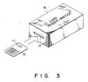
- Fig. 3 shows an outer appearance of IC card reader/writer 16 used in a terminal for an issuer dealing with IC card 10, e.g., a personal computer. More specifically, reader/writer 16 is electrically connected to contacts portion 11 of IC card 10 inserted from card slot 17, and reads or writes data from or in a memory of IC card 10.
- IC card reader/writer 16 is connected to a main body (Fig. 1) of personal computer PC through a cable.
- the electrical circuit comprises contacts portion 11; communication circuit 21; reset circuit 22; power supply regulator 23; internal battery (built-in battery) 25 of, e.g., 3 V; battery checker 24 for checking if a voltage value of built-in battery 25 is equal to or higher than a rated value; clock controller 26; oscillator 27, as an arithmetic clock quartz oscillator, for outputting a signal at an oscillation frequency of 200 kHz (high-speed clock); control CPU (central processing unit) 28; program ROM 29 for storing a control program; work memory 30 for a program; data memory 31, comprising a PROM, for storing an ID number, data, and the like; timer 32 used for measuring time during a processing operation; calender circuit 33; oscillator (clock generation means) 34, as a fundamental clock quartz oscillator, for outputting a signal at an oscillation frequency of 32.768 kHz (low-speed
- Communication circuit 21, CPU 28, ROM 29, work memory 30, data memory 31, timer 32, calender circuit 33, display controller 35, and keyboard interface 38 are connected to each other through data bus 20.
- communication circuit 21 converts serial I/O signals supplied from terminal 16 through contacts portion 11 into parallel data, and outputs it onto data bus 20.
- circuit 21 converts parallel data supplied from data bus 20 into serial I/O signals, and outputs them to terminal 16 through contacts portion 11. In this case, the format content of conversion is determined by terminal 16 and IC card 10.
- Reset circuit 22 generates a reset signal to start CPU 28 when the on-line mode is set.
- Power supply regulator 23 switches a drive mode from one by built-in battery 25 to the other by an external power supply after the lapse of a predetermined period of time from the beginning of the on-line mode.
- regulator 23 switches the drive mode from one by the external power supply to the other by builtin battery 25.
- Clock controller 26 appropriately switches the low-and high-speed clocks in the off-line mode in which a card operation is performed by built-in battery 25.
- controller 26 stops oscillator 27 which outputs a signal of an oscillation frequency of 200 kHz (high-speed clock), thereby stopping supply of a clock signal to CPU 28. Then, controller 26 waits in a perfect HALT state.
- Clock controller 26 basically selects a timepiece clock (32.768 kHz) upon execution of the HALT command.
- Calender circuit 33 has a timepiece (timer 32) which can be desirably set and updated by a card holder, and a transaction timepiece (counter 100) in which a world standard time is set upon issuance of the card and cannot be changed.
- Display controller 35 converts display data supplied from CPU 28 into a character pattern using character generator 350 comprising an internal ROM, and displays the character pattern on display unit 13 using display driver 36.
- Keyboard interface 38 converts an input at keyboard 12 into a corresponding key input signal, and outputs it to CPU 28.
- calender circuit 33 The main part of calender circuit 33 will be described in detail below with reference to Fig. 1. More specifically, an oscillation start reset signal supplied from an external device (e.g., a pulse generator; not shown) in the manufacture of card 10, or a restart command output from CPU 28 is supplied to select input S of drive power supply switcher (supply means) 42 through logical OR circuit 41. Switcher 42 is supplied with power supply voltage Vdd from built-in battery 25, and power supply voltage Vdd/2 from voltage generator 50 (to be described later).
- an oscillation start reset signal supplied from an external device e.g., a pulse generator; not shown
- a restart command output from CPU 28 is supplied to select input S of drive power supply switcher (supply means) 42 through logical OR circuit 41.
- Switcher 42 is supplied with power supply voltage Vdd from built-in battery 25, and power supply voltage Vdd/2 from voltage generator 50 (to be described later).
- drive power supply switcher 42 When drive power supply switcher 42 receives the reset signal or the restart command, it outputs power supply voltage Vdd from built-in battery 25; when it receives neither of these signals, it outputs power supply voltage Vdd/2 from voltage generator 50.
- the reset signal or the restart command is supplied for, e.g., 1 sec until a circuit operation of card 10 is stabilized after card 10 is started.
- the output from switcher 42 is supplied to oscillation circuit 43.
- Oscillation circuit 43 oscillates a clock signal of 32.768 kHz in accordance with power supply voltage Vdd or Vdd/2 selectively supplied from switcher 42.
- Oscillation circuit 43 comprises oscillator 34 having an oscillation frequency of 32.768 kHz, resistor 45 capacitors 46 and 47, and inverters 48 and 49.
- Clock signal CK generated by oscillation circuit 43 is supplied to voltage generator 50, and is also supplied to counter 100 and clock controller 26.
- Voltage generator 50 is a circuit for generating voltage Vdd/2 half the power supply voltage of built-in battery 25 in accordance with clock signal CK from oscillation circuit 43, and has an arrangement, as shown in, e.g., Fig. 1A. More specifically, NPN bipolar transistor (switching element) Tr1 is enabled/disabled in response to clock signal CK having a duty cycle of 50% which is input to its base through resistor R1. The emitter of transistor Tr1 is grounded, and its collector is connected to power supply Vdd through resistor R2 and to the base of NPN transistor Tr2. The collector of transistor Tr2 is applied with power supply voltage Vdd, and its emitter is grounded through capacitor Cd.
- NPN bipolar transistor (switching element) Tr1 is enabled/disabled in response to clock signal CK having a duty cycle of 50% which is input to its base through resistor R1.
- the emitter of transistor Tr1 is grounded, and its collector is connected to power supply Vdd through
- Capacitor Cd is charged by an emitter current of ON transistor Tr2 for half a period of clock signal CK in which transistor Tr1 is kept OFF. Capacitor Cd is discharged through a load powered by a charge accumulated in capacitor Cd for the other half period of clock CK. Capacitor Cd repeats charging and discharging every half periods of clock signal CK, so that a voltage of an average of almost Vdd/2 appears across capacitor Cd.
- Power supply voltage Vdd/2 output from voltage generator 50 is supplied to drive power supply switcher 42, and also to data bus 20.
- CPU 28 executes the content of program ROM 29 from its address "0" in response to the external clock.
- CPU 28 in IC card 10 checks the state of external voltage Vcc. If CPU 28 determines that external voltage Vcc has a sufficient level, and a power-down mode for detecting a decrease in external voltage is not set, it executes an on-line mode program.
- a data communication format prepared in IC card 10 is sent to terminal 16 first, and an instruction from terminal 16 is then waited.
- terminal 16 When terminal 16 normally receives communication mode data, it outputs the restart command to calender circuit 33 in IC card 10. Thus, calender circuit 33 restarts oscillation of oscillation circuit 43 in accordance with the restart command.
- the restart command is supplied to select input S of drive power supply switcher 42 through OR circuit 41.
- Drive power supply switcher 42 selects power supply voltage Vdd from built-in battery 25 and outputs it to oscillation circuit 43 while the restart command is supplied.
- Oscillation circuit 43 oscillates a clock signal of 32.768 kHz in accordance with power supply voltage Vdd applied from drive power supply switcher 42.
- the clock signal from oscillation circuit 43 is supplied to voltage generator 50.
- Voltage generator 50 outputs power supply voltage Vdd/2 to switcher 42 in accordance with the input clock signal.
- switcher 42 selects power supply voltage Vdd/2 from voltage generator 50, and outputs it to oscillation circuit 43.
- Oscillation circuit 43 then oscillates a clock signal of 32.768 kHz in accordance with power supply voltage Vdd/2 applied from drive power supply switcher 42.
- a signal (answer-to-list) is sent from terminal 16 to card 10 through communication circuit 21 shown in Fig. 4 (ST52).
- CPU 28 in card 10 Upon reception of this signal, CPU 28 in card 10 outputs the restart command (ST53).
- Power supply switcher 42 shown in Fig. 1 then switches an operation voltage of card 10 from Vdd/2 for a power save mode to Vdd for a normal operation mode. In the normal operation mode, card 10 performs on-line processing with a host computer or the like (not shown) through terminal 16 (ST54).
- the restart command is forcibly sent to IC card 10.
- the present invention is not limited to this.
- the restart command may be sent to IC card 10.
- terminal 16 when terminal 16 normally receives communication mode data, it outputs an output request of a power supply voltage from voltage generator 50 to CPU 28 in IC card 10. Then, CPU 28 transmits the power supply voltage from voltage generator 50 in calender circuit 33 to terminal 16 through data bus 20, communication circuit 21, and contacts portion 11.
- terminal 16 When the power supply voltage from voltage generator 50 is kept OFF, terminal 16 outputs the restart command to calender circuit 33 in IC card 10. Then, calender circuit 33 restarts oscillation of oscillation circuit 43 in accordance with the restart command, as described above.
- terminal 16 When the power supply voltage from voltage generator 50 is not OFF, terminal 16 outputs a time read request to CPU 28 in IC card 10. In this case, CPU 28 transmits time in calender circuit 33 to terminal 16 through data bus 20, communication circuit 21, and contacts portion 11.
- terminal 16 When the input time is considerably different from actual time by, e.g., several hours, terminal 16 outputs the restart command to calender circuit 33 in IC card 10. Calender circuit 33 restarts oscillation of oscillation circuit 43 in accordance with the restart command, as described above.
- a signal (answer-to-list) is sent from terminal 16 to card 10 through communication circuit 21 shown in Fig. 4 (ST62).
- inverter 61 and flip-flop 62 (Fig. 7) in card 10 read a logic value of Vdd/2 based on the presence/absence of a voltage from a Vdd/2 circuit (ST63).
- a rated value of Vdd/2 is 1.5 V
- a voltage of 1.0 V or more is read as logic "1”
- a voltage of less than 1.0 V is read as logic "0".
- CPU 28 reads clock data from timer 32 shown in Fig. 4 (ST67).
- the clock data is verified using reference clock data (output from counter 100 shown in Fig. 1) (ST68).
- the restart command is output (ST65), and on-line processing is then executed (ST66).
- ST66 On-line processing is immediately started (ST66).
- the oscillator of the IC card is stopped by a shock when the card is dropped, the oscillator is restarted by the restart command from the terminal, and the function of the IC card is resumed.
- the present invention is not limited to this.
- the oscillator of the IC card is stopped by a shock when the card is dropped, the restart operation can be performed by the IC card itself.
- calender circuit 33 is arranged as shown in Fig. 7.
- the same reference numerals in Fig. 7 denote the same parts as in Fig. 1, and a detailed description thereof will be omitted.
- a power supply voltage output from voltage generator 50 to drive power supply switcher 42 is supplied to the set input terminal of flip-flop 62, and is also input to the reset input terminal thereof through inverter 61.
- the set output of this flip-flop 62 is supplied to select input S of switcher 42.
- OR circuit 63 receives an oscillation start reset signal supplied from an external device (e.g., PC in Fig. 1) upon manufacture of IC card 10.
- switcher 42 While the restart signal is supplied, switcher 42 outputs power supply voltage Vdd from built-in battery 25 to oscillation circuit 43.
- oscillation circuit 43 oscillates a clock signal of 32.768 kHz in accordance with power supply voltage Vdd applied from switcher 42.
- the clock signal from oscillation circuit 43 is supplied to voltage generator 50.
- Voltage generator 50 outputs power supply voltage Vdd/2 to switcher 42 in accordance with the input clock signal.
- switcher 42 selects power supply voltage Vdd/2 from voltage generator 50, and outputs it to oscillation circuit 43.
- Oscillation circuit 43 then oscillates a clock signal of 32.768 kHz in accordance with power supply voltage Vdd/2 applied from drive power supply switcher 42.
- an IC card is used.
- the present invention is not limited to this.
- a portable electronic device need not have a card-like shape but may have other shapes, e.g., a rod-like shape as long as it has a data memory and a control element, and can selectively perform I/Os from an external device.
- a portable electronic device which can restart an oscillator using a circuit with small current consumption when oscillation of the oscillator is stopped by some shock, and can prevent stop of the device function.
Landscapes
- Engineering & Computer Science (AREA)
- Theoretical Computer Science (AREA)
- Physics & Mathematics (AREA)
- General Engineering & Computer Science (AREA)
- General Physics & Mathematics (AREA)
- Power Sources (AREA)
- Credit Cards Or The Like (AREA)
- Electric Clocks (AREA)
- Dc-Dc Converters (AREA)
Applications Claiming Priority (2)
| Application Number | Priority Date | Filing Date | Title |
|---|---|---|---|
| JP1143828A JP2723296B2 (ja) | 1989-06-06 | 1989-06-06 | 携帯可能媒体 |
| JP143828/89 | 1989-06-06 |
Publications (3)
| Publication Number | Publication Date |
|---|---|
| EP0401806A2 true EP0401806A2 (de) | 1990-12-12 |
| EP0401806A3 EP0401806A3 (de) | 1993-03-03 |
| EP0401806B1 EP0401806B1 (de) | 1997-08-13 |
Family
ID=15347893
Family Applications (1)
| Application Number | Title | Priority Date | Filing Date |
|---|---|---|---|
| EP90110738A Expired - Lifetime EP0401806B1 (de) | 1989-06-06 | 1990-06-06 | Tragbares elektronisches Gerät mit einer Stromquelle |
Country Status (4)
| Country | Link |
|---|---|
| US (1) | US5105074A (de) |
| EP (1) | EP0401806B1 (de) |
| JP (1) | JP2723296B2 (de) |
| DE (1) | DE69031249T2 (de) |
Cited By (2)
| Publication number | Priority date | Publication date | Assignee | Title |
|---|---|---|---|---|
| EP0709785A3 (de) * | 1994-10-27 | 1998-08-12 | Oki Electric Industry Co., Ltd. | Gerät zur internen Zustandsbestimmung |
| US5849816A (en) * | 1994-08-01 | 1998-12-15 | Leonard Pearlstein | Method of making high performance superabsorbent material |
Families Citing this family (14)
| Publication number | Priority date | Publication date | Assignee | Title |
|---|---|---|---|---|
| DK174975B1 (da) * | 1988-05-06 | 2004-04-05 | Toppan Printing Co Ltd | Integreret kredsløbskort |
| FR2654232A1 (fr) * | 1989-11-07 | 1991-05-10 | Europ Rech Electr Lab | Generateur de tensions continues pour l'alimentation d'une carte a circuit integre. |
| US5274221A (en) * | 1990-06-22 | 1993-12-28 | Mitsubishi Denki Kabushiki Kaisha | Non-contact integrated circuit card |
| JP2822624B2 (ja) * | 1990-07-03 | 1998-11-11 | 三菱電機株式会社 | 非接触icカード |
| JP2549192B2 (ja) * | 1990-09-19 | 1996-10-30 | 三菱電機株式会社 | 非接触icカード及びその使用方法 |
| JP2842750B2 (ja) * | 1992-04-07 | 1999-01-06 | 三菱電機株式会社 | Icカード |
| USD350120S (en) | 1992-08-24 | 1994-08-30 | Kabushiki Kaisha Toshiba | Combined reader and writer for information recording cards |
| EP0599244B1 (de) * | 1992-11-27 | 1999-04-14 | Denso Corporation | Tragbares elektronisches Gerät |
| JPH0721336A (ja) * | 1993-07-05 | 1995-01-24 | Mitsubishi Electric Corp | 接触型携帯機器及び非接触型携帯機器 |
| JP3430866B2 (ja) * | 1997-07-16 | 2003-07-28 | 株式会社デンソー | 電源低下対応装置 |
| DE10007284A1 (de) * | 2000-02-17 | 2001-08-23 | Orga Kartensysteme Gmbh | Chipkarte |
| US8212631B2 (en) | 2008-03-13 | 2012-07-03 | Viasat, Inc. | Multi-level power amplification system |
| KR101685389B1 (ko) * | 2010-10-08 | 2016-12-20 | 삼성전자주식회사 | 스마트 카드 |
| DE102013104142B4 (de) * | 2013-04-24 | 2023-06-15 | Infineon Technologies Ag | Chipkarte |
Family Cites Families (7)
| Publication number | Priority date | Publication date | Assignee | Title |
|---|---|---|---|---|
| US4320387A (en) * | 1978-12-28 | 1982-03-16 | Powell William S | Information communicating apparatus and method |
| GB2065391B (en) * | 1979-12-05 | 1984-05-10 | Casio Computer Co Ltd | Power supply system |
| JPS56126788A (en) * | 1980-03-12 | 1981-10-05 | Ricoh Elemex Corp | Power supply circuit for timepiece |
| US4766294A (en) * | 1986-08-29 | 1988-08-23 | Kabushiki Kaisha Toshiba | Portable medium |
| US4814591A (en) * | 1987-04-13 | 1989-03-21 | Kabushiki Kaisha Toshiba | Portable medium |
| JPS63198567U (de) * | 1987-06-12 | 1988-12-21 | ||
| JPH0610830B2 (ja) * | 1988-04-09 | 1994-02-09 | シャープ株式会社 | Icカードのクロック信号切換装置 |
-
1989
- 1989-06-06 JP JP1143828A patent/JP2723296B2/ja not_active Expired - Lifetime
-
1990
- 1990-06-06 US US07/534,483 patent/US5105074A/en not_active Expired - Fee Related
- 1990-06-06 DE DE69031249T patent/DE69031249T2/de not_active Expired - Fee Related
- 1990-06-06 EP EP90110738A patent/EP0401806B1/de not_active Expired - Lifetime
Cited By (2)
| Publication number | Priority date | Publication date | Assignee | Title |
|---|---|---|---|---|
| US5849816A (en) * | 1994-08-01 | 1998-12-15 | Leonard Pearlstein | Method of making high performance superabsorbent material |
| EP0709785A3 (de) * | 1994-10-27 | 1998-08-12 | Oki Electric Industry Co., Ltd. | Gerät zur internen Zustandsbestimmung |
Also Published As
| Publication number | Publication date |
|---|---|
| JPH039414A (ja) | 1991-01-17 |
| JP2723296B2 (ja) | 1998-03-09 |
| DE69031249T2 (de) | 1998-03-19 |
| DE69031249D1 (de) | 1997-09-18 |
| US5105074A (en) | 1992-04-14 |
| EP0401806A3 (de) | 1993-03-03 |
| EP0401806B1 (de) | 1997-08-13 |
Similar Documents
| Publication | Publication Date | Title |
|---|---|---|
| US5168151A (en) | Portable electronic device having a memory with restricted access in off-line modes | |
| US5105074A (en) | Power supply reliability of portable electronic device | |
| US5072103A (en) | Electrically powered portable medium | |
| EP0257648B1 (de) | Tragbarer Datenträger | |
| US4814591A (en) | Portable medium | |
| US4924075A (en) | Smart IC card | |
| US4827111A (en) | Intelligent-type IC card containing IC circuit and battery | |
| JPH0962804A (ja) | Icカードリーダ | |
| EP0306821B1 (de) | Elektronisches Gerät mit Kalenderfunktion | |
| JP2791105B2 (ja) | 携帯可能記憶媒体 | |
| JP2597553B2 (ja) | Icカード | |
| JPH0746294B2 (ja) | 携帯可能電子装置 | |
| JPH036718A (ja) | 携帯可能媒体 | |
| JPS6358520A (ja) | 携帯可能媒体 | |
| JPS63262783A (ja) | 携帯可能媒体 | |
| JPH01126787A (ja) | 携帯可能媒体 | |
| JPS63262781A (ja) | 携帯可能媒体 | |
| JPS63255785A (ja) | 携帯可能媒体 | |
| JPS6362086A (ja) | Icカード | |
| JPH0314052A (ja) | 携帯可能媒体 | |
| JPH01112350A (ja) | 携帯可能媒体 | |
| JPH03193399A (ja) | 携帯可能媒体 | |
| JPS63255784A (ja) | 携帯可能媒体 | |
| JPH01112389A (ja) | 携帯可能媒体 | |
| JPH01112390A (ja) | 携帯可能媒体 |
Legal Events
| Date | Code | Title | Description |
|---|---|---|---|
| PUAI | Public reference made under article 153(3) epc to a published international application that has entered the european phase |
Free format text: ORIGINAL CODE: 0009012 |
|
| 17P | Request for examination filed |
Effective date: 19900606 |
|
| AK | Designated contracting states |
Kind code of ref document: A2 Designated state(s): DE FR |
|
| PUAL | Search report despatched |
Free format text: ORIGINAL CODE: 0009013 |
|
| AK | Designated contracting states |
Kind code of ref document: A3 Designated state(s): DE FR |
|
| 17Q | First examination report despatched |
Effective date: 19950302 |
|
| GRAG | Despatch of communication of intention to grant |
Free format text: ORIGINAL CODE: EPIDOS AGRA |
|
| GRAH | Despatch of communication of intention to grant a patent |
Free format text: ORIGINAL CODE: EPIDOS IGRA |
|
| GRAH | Despatch of communication of intention to grant a patent |
Free format text: ORIGINAL CODE: EPIDOS IGRA |
|
| GRAA | (expected) grant |
Free format text: ORIGINAL CODE: 0009210 |
|
| AK | Designated contracting states |
Kind code of ref document: B1 Designated state(s): DE FR |
|
| REF | Corresponds to: |
Ref document number: 69031249 Country of ref document: DE Date of ref document: 19970918 |
|
| ET | Fr: translation filed | ||
| PLBE | No opposition filed within time limit |
Free format text: ORIGINAL CODE: 0009261 |
|
| STAA | Information on the status of an ep patent application or granted ep patent |
Free format text: STATUS: NO OPPOSITION FILED WITHIN TIME LIMIT |
|
| 26N | No opposition filed | ||
| PGFP | Annual fee paid to national office [announced via postgrant information from national office to epo] |
Ref country code: DE Payment date: 19990607 Year of fee payment: 10 |
|
| PGFP | Annual fee paid to national office [announced via postgrant information from national office to epo] |
Ref country code: FR Payment date: 19990610 Year of fee payment: 10 |
|
| PG25 | Lapsed in a contracting state [announced via postgrant information from national office to epo] |
Ref country code: FR Free format text: LAPSE BECAUSE OF NON-PAYMENT OF DUE FEES Effective date: 20010228 |
|
| REG | Reference to a national code |
Ref country code: FR Ref legal event code: ST |
|
| PG25 | Lapsed in a contracting state [announced via postgrant information from national office to epo] |
Ref country code: DE Free format text: LAPSE BECAUSE OF NON-PAYMENT OF DUE FEES Effective date: 20010403 |