EP0401855B1 - Détecteur d'erreurs de blocs - Google Patents
Détecteur d'erreurs de blocs Download PDFInfo
- Publication number
- EP0401855B1 EP0401855B1 EP90110890A EP90110890A EP0401855B1 EP 0401855 B1 EP0401855 B1 EP 0401855B1 EP 90110890 A EP90110890 A EP 90110890A EP 90110890 A EP90110890 A EP 90110890A EP 0401855 B1 EP0401855 B1 EP 0401855B1
- Authority
- EP
- European Patent Office
- Prior art keywords
- data
- block
- mode
- counters
- detector
- Prior art date
- Legal status (The legal status is an assumption and is not a legal conclusion. Google has not performed a legal analysis and makes no representation as to the accuracy of the status listed.)
- Expired - Lifetime
Links
Images


Classifications
-
- H—ELECTRICITY
- H04—ELECTRIC COMMUNICATION TECHNIQUE
- H04N—PICTORIAL COMMUNICATION, e.g. TELEVISION
- H04N5/00—Details of television systems
- H04N5/76—Television signal recording
- H04N5/91—Television signal processing therefor
- H04N5/93—Regeneration of the television signal or of selected parts thereof
- H04N5/94—Signal drop-out compensation
- H04N5/945—Signal drop-out compensation for signals recorded by pulse code modulation
-
- G—PHYSICS
- G11—INFORMATION STORAGE
- G11B—INFORMATION STORAGE BASED ON RELATIVE MOVEMENT BETWEEN RECORD CARRIER AND TRANSDUCER
- G11B20/00—Signal processing not specific to the method of recording or reproducing; Circuits therefor
- G11B20/10—Digital recording or reproducing
-
- G—PHYSICS
- G11—INFORMATION STORAGE
- G11B—INFORMATION STORAGE BASED ON RELATIVE MOVEMENT BETWEEN RECORD CARRIER AND TRANSDUCER
- G11B20/00—Signal processing not specific to the method of recording or reproducing; Circuits therefor
- G11B20/10—Digital recording or reproducing
- G11B20/18—Error detection or correction; Testing, e.g. of drop-outs
Definitions
- the present invention relates to a block error detector, and more particularly, to a detector for detecting error in storing position of a block data use, for example, in digital video data.
- a block error detector for detecting an error in data blocks in accordance with the preamble of claim 1 is known from GB-A-20 84 363.
- the device according to this document further comprises reading address generator means for generating a section reading address at a predetermined frequency for designating a section in said memory means, and for generating a segment reading address for designating a segment in the designated section, switching means for switching between writing mode in which block data is written into said memory means by the control of said writing address generator means, and reading mode in which the block data is read out from said memory means by the control of said reading address generator means, said switching means further switching said counters in a first mode Operaation during said writing mode and a second mode operation during said reading mode operation.
- said counters are in count up mode during said first mode operation, and in count down mode during said second mode operation; said counters being in count up mode during said first mode operation, and are in shift mode for shifting their contents to said detector means during said second mode operation.
- data blocks B0, B1, B3, ... such as that shown in Fig. 1 represent a known recording pattern for recording digital data, such as digital video data.
- Each block is composed of a number of sub-blocks, each sub-block carrying different information.
- the first sub-block at the very beginning of the block carries a sync data of two words long (one word is eight bit long).
- the second sub-block carries ID data of four words.
- the third sub-block carries image data of 240 words, and the fourth sub-block carries parity check data of four words.
- the data length are given merely as an example.
- the ID data includes, for example, a specific horizontal scan line. Therefore, the image data following the ID data will be used for filling the horizontal line identified by the ID data.
- the parity check data includes the parity information required for error correction of the ID data and/or any other data in each block.
- the sync data is first detected, and then the ID data is read out all or partially.
- the read ID data is used to define an address in a memory for storing image data. Then, the image data is read out and stored in the memory at a particular area identified by the address formed by the detected ID data.
- the ID data when there is an error in the detected ID data, the ID data will designate wrong area in the memory. Thus, the image data following the ID data will be stored in the wrong area.
- the digital VCR available at present are mostly for business use or for professional use and, therefore, the digital VCR is equipped with a high grade arrangement which scarcely produces error. Therefore, even if an error is produced in the ID data, such an error can be easily corrected by the known error correction system, one of which is the parity check system.
- the digital VCR for the private use or home use as will be released in the market near future requires a high density recording system so as to enable long VCR recording time. Therefore, the rate of generation of error becomes great, resulting in serious defects, particularly when the error occurs in the ID data, as explained below.
- the address defined by such ID data will provide a wrong address.
- the image data following the ID data will be stored in a wrong area in the memory.
- data regenerator results in a block error.
- this error cannot be corrected with the parity information. For example, when the ID data which should represent a location A but erroneously represents a location B, the image data will not be written to the memory area corresponding to location A, and the contents of that memory area will not be renewed properly.
- the non-renewed image data i.e., the old image data which was stored in the previous loading cycle
- the data parity information also refers to this non-renewed data, it is not possible to determine whether the data read was the non-renewed data or not.
- the prior art digital data processor is thus not able to detect errors resulting from various causes using the parity information in the data block itself.
- the present invention has been developed with a view to substantially solving the above described disadvantages and has for its essential object to provide a block error detector which can detect an error occurring in the ID data.
- a train of data blocks each carrying digital data and ID data are produced from reading head as a tape passes the cylinder.
- a memory having a plurality of sections is provided, and a plurality of counters are provided correspondingly to the sections.
- the digital data are stored in a memory at a second identified by the ID data.
- a counter corresponding to that section is incremented, and each time the digital data for one block is read out from a section in the memory, a counter corresponding to that section is decreased.
- the block error detector for detecting an error in data blocks comprises a memory having a plurality of sections, each section having a plurality of segments for storing information signals for a plurality of data blocks.
- a writing address generator means is provided for generating a section writing address based on the ID block for designating a section in the memory means, and for generating a segment writing address for designating a segment in the designated section.
- a plurality of counters are provided correspondingly to the plurality of sections, respectively, and operated in response to the section writing address. Also, a detector means is provided for receiving counted results of said counters.
- the detector means detects an error in said ID block when all the counters, which are all supposed to be incremented by "1" when all the ID data are properly detected, are not incremented by "1".
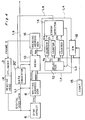
- a block error detector according to a preferred embodiment of the present invention is shown as employed in a digital video cassette recorder which has a cylinder 2 mounted with one or more recording heads 4.
- the reading head 4 reads digital video data stored on a cassette tape as it passes along the rotating cylinder 2.
- the digital video data is shown in Fig. 1 and which includes data blocks B0, B1, B2, ... aligned serially.
- Each block is composed of a number of sub-blocks, each sub-block carrying different information.
- the first sub-block, at the very beginning of the block carries a sync data of two words long (one word is eight bit long).
- the second sub-block carries ID data of four words.
- the third sub-block carries image data of 241 words, and the fourth sub-block carries parity check data of four words.
- the data length are given merely as an example.
- the ID data includes, for example, a specific horizontal scan line. Therefore, the image data following the ID data will be used for filling the horizontal line identified by the ID data.
- the block error detector includes a sync detector 6, a writing address generator 8 and a memory 10, which are connected in series and are also connected with a line L1 carrying the digital video data from reading head 4.
- Sync detector 6 detects the sync data at the very beginning of each data block. When the sync data is detected, sync detector 6 activates write address generator 8 to receive the ID data following the sync data.
- the writing address generator 8 Upon receipt of the ID data, the writing address generator 8 forms and produces a write block address (WBA) and write data address (WDA) for specifying an area in the memory 10 in which the image data following the ID data is stored.
- WBA write block address
- WDA write data address
- the WBA represents vertical address Yi
- WDA represents horizontal address Xi.
- the ID data is used for defining the address of a segment from which the storing starts. For example, when the data block B0 is produced from reading head 4, the address that will be formed by the writing address generator 8 with reference to ID data in data block B0 will be (Y0, X0). Thus, the first word D0 in the image data will be stored in segment (Y0, X0) in memory 10.
- the writing address generator 8 produces next address (Y0, X1).
- the second word D1 in the image data will be stored in segment (Y0, X1).
- the writing address generator 8 sequentially produces addresses (Y0, X0), (Y0, X1), (Y0, X2), (Y0, X3), ... (Y0, X239) and (Y0, X240) so that image data D0, D1, D2, ... D239 and D240 are stored in the first row as shown in Fig. 3.
- the WBA represents vertical address Yi and WDA represents horizontal address Xi
- the WBA represents block address Yi for specifying a block in which the hole data block is to be stored
- WDA represents data address Xi for specifying each segment in which the respective image data is to be stored.
- memory 10 has a capacity for carrying N+1 data blocks.
- N+1 is equal to 16.
- the block address WBA which is Yi in the above example, is also applied to a switching circuit 18 through line L2 and further to selector 12 through line L3.
- Switching circuit 18 is controlled by a control 15 such that line L2 is connected to L3 at the beginning of each data block, such as immediately after the generation of ID data.
- Selector 12 has N outputs T0, T1, ... TN which are connected to counters C0, C1, ... CN, respectively.
- Counters C0, C1, ... CN have output terminals which are connected to an error detector 14, and control terminals which are connected to control 15, which also controls between writing mode operation and reading mode operation. During the writing mode operation, counters C0 - CN are switched to count up state, and during the reading mode operation, counters C0 - CN are switched to count down state.
- the output of error detector 14 is connected to a data converter 20 which is inserted in a line L6 extending from an output of memory 10.
- a reading address generator 16 which has a similar structure to that of writing address generator 8, produces reading block address (RBA) and reading data address (RDA) which are applied to memory 10.
- RBA is also applied to switching circuit 18 through line L4.
- the RBA and RDA are produced relatively to the frame signal which is also applied to the cylinder 2 for controlling the generation of the digital video data.
- the frame signal is in relation to the sync data.
- memory 10 is originally stored with no data, and counters C1 to CN are reset to zero.
- control 15 is set to writing mode so that writing address generator 8 is activated and memory 10 is set to a condition for storing image data through line L1.
- writing address generator 8 sequentially generates addresses (Y0, X0), (Y0, X1), (Y0, X2), (Y0, X3), ... (Y0, X239) and (Y0, X240) so that image data D0, D1, D2, ... D239 and D240 are stored in the first row as shown in Fig. 3.
- switching unit 18 is operated to connected line L2 line L3 at the beginning of the first data block B0, such as during when the writing address generator 8 is producing the first address (Y0, X0).
- the writing block address in this case Y0
- selector 12 In response to WBA Y0, selector 12 produces a pulse from its first output terminal T0 so that counter C0 counts up to "1".
- writing address generator 8 sequentially generates addresses (Y1, X0), (Y1, X1), (Y1, X2), (Y1, X3), ... (Y1, X239) and (Y1, X240) so that image data D0, D1, D2, ... D239 and D240 are stored in the second row.
- switching circuit 18 is operated to connected line L2 with line L3 at the beginning of the second data block B1, such as during when the writing address generator 8 is producing the first address (Y1, X0).
- the writing block address in this case Y1 is applied to selector 12.
- selector 12 produces a pulse from its second output terminal T1 so that counter C1 counts up to "1".
- error detector 14 detects the contents of counters C0 - CN. In the above described case, since all the counters C0 - CN are incremented to "1", error detector detects that no error has been occurred in any of the blocks during the writing of the data in memory 10.
- control 15 is set to reading mode so that reading address generator 16 is activated and memory 10 is set to a condition for reading out stored image data through line L6.
- reading address generator 16 sequentially generates, in response to a field signal (this signal is in relation to sync signal and is also in relation to the frame signal), addresses (Y0, X0), (Y0, X1), (Y0, X2), (Y0, X3), ... (Y0, X239) and (Y0, X240) so that image data D0, D1, D2, ... D239 and D240 stored in the first row are sequentially transmitted through line L6 to data converter 20.
- switching circuit 18 is operated to connected line L4 with line L3 at the beginning of the first data block B0, such as during when the reading address generator 16 is producing the first address (Y0, X0).
- the reading block address in this case Y0
- selector 12 In response to WBA Y0, selector 12 produces a pulse from its first output terminal T0 so that counter C0 counts down to "0".
- reading address generator 16 sequentially generates addresses (Y1, X0), (Y1, X1), (Y1, X2), (Y1, X3), ... (Y1, X239) and (Y1, X240) so that image data D0, D1, D2, ... D239 and D240 stored in the second row are sequentially transmitted through line L6 to data converter 20.
- switching circuit 18 is operated to connected line L4 with line L3 at the beginning of the second data block B1, such as during when the reading address generator 16 is producing the first address (Y1, X0).
- the reading block address in this case Y1 is applied to selector 12.
- selector 12 produces a pulse from its second output terminal T1 so that counter C1 counts down to "0".
- error detector 14 detects the contents of counters C0 - CN. In the above described case, since all the counters C0 - CN are decreased to "0", error detector detects that no error has been occurred in any of the blocks during the reading of the data as stored in memory 10.
- the writing address generator 8 sequentially generates addresses (Y?, X0), (Y?, X1), (Y?, X2), (Y?, X3), ... (Y?, X239) and (Y?, X240) so that image data D0, D1, D2, ... D239 and D240 for the second data block B1 will not be stored in any row in memory 10.
- the second row in memory 10 remains blank or remains with old data.
- counters C0 and C2 - CN are incremented to "1", but leaving counter C1 as "0".
- error detector 14 detects that the second row in the memory 10 is not renewed with the new image data.
- the writing address generator 8 sequentially generates addresses (Y2, X0), (Y2, X1), (Y2, X2), (Y2, X3), ... (Y2, X239) and (Y2, X240) so that image data D0, D1, D2, ... D239 and D240 are stored in the third row, resulting in the skip of the second row, as shown in Fig. 3.
- counter C2 is incremented to "1", but leaving counter C1 as "0".
- the writing address generator 8 sequentially generates addresses (Y2, X0), (Y2, X1), (Y2, X2), (Y2, X3), ... (Y2, X239) and (Y2, X240) so that image data D0, D1, D2, ... D239 and D240 are stored in the third row, resulting in correct data insertion in the third row over the data just entered by the previous data block.
- counter C2 is further incremented to "2", and yet leaving counter C1 as "0".
- error detector 14 detects that the second row in the memory 10 is not renewed with the new image data, and the third row is renewed twice.
- the detected error signal is transmitted from error detector 14 through line L5 to data converter 20 which carries out a data compensation process to correct the image data in the error block in the known manner.
- the horizontal line with error image data caused by the incorrect ID data may be replaced with a neighboring horizontal line, or with the same horizontal line but obtained in a previous cycle.
- control 15 may be so arranged to provide writing mode and reading mode signals in an interlaced manner so that the writing mode and reading mode operations are carried out in an interlaced manner.
- error detector 14 is so arranged as to incorporate N+1 registers to receive contents of counters C0 - CN.
- switching circuit 18 operates such that after the writing mode for writing N data blocks, the contents of each counter is sequentially shifted from the counter to corresponding register in response to each reading block address. For example, when a first reading block address Y0 is produced from reading address generator 16, Y0 is transmitted through lines L4 and L3 to error detector 14 so that the first register in error detector 14 is activated to receive the contents of counter C0. After the contents of the counter C0 is shifted to the corresponding register, the counter C0 is reset to zero. In this manner, the contents of the counters are shifted sequentially to the registers.
- the data converter 20' is inserted in line L1, as shown in Fig. 4.
- the data error correction can be carried out before the image data is stored in memory 10.
- the counters C0-CN can be so arranged as to provide only ony counter and n+1 registers coupled to the counter.
- the present invention is able to detect errors in ID data by the use of the counters and error detector 14.
- the block parity can be mainly used for correcting data other than the ID data.
- the invention is not only limited for use in digital VCR, but can be used in other digital data transfer system in which the data are arranged in blocks.
Landscapes
- Engineering & Computer Science (AREA)
- Signal Processing (AREA)
- Multimedia (AREA)
- Television Signal Processing For Recording (AREA)
- Signal Processing For Digital Recording And Reproducing (AREA)
Claims (6)
- Un détecteur d'erreur de bloc pour la détection d'une erreur dans des blocs de données, chaque bloc comportant des sous-blocs de bloc ID et de bloc d'informations comprenant une pluralité de signaux d'informations (D0, D1, D2,...), ledit détecteur d'erreur de bloc comprenant :un moyen de mémoire (10) ayant une pluralité de sections (Y0, Y1, Y2,...) et chaque section ayant une pluralité de segments (X0, X1, X2,...) pour stocker des signaux d'informations pour une pluralité de blocs de données;un moyen générateur d'adresse d'écriture (8) pour la génération d'une adresse d'écriture de section (WBA) basé sur ledit bloc ID pour désigner une section dans ledit moyen de mémoire (8) et pour la génération d'une adresse d'écriture de segment (WDA) pour désigner un segment dans la section désignée;une pluralité de compteurs (C0, C1, C2,...) sont pourvus respectivement en correspondance avec ladite pluralité de sections, et mis en fonctionnement en réponse à ladite adresse d'écriture de section; etun moyen détecteur (14) pour recevoir des résultats de comptage desdits compteurs (C0, C1, C2,...), par quoi ledit moyen de détecteur (14) détecte une erreur dans ledit block ID lorsque tous les compteurs, qui sont tous supposés être incrémentés par "1" lorsque toutes les données ID sont détectées correctement, ne sont pas incrémentés par "1", caractérisé en ce que le détecteur d'erreur de bloc comprend d'autre part un convertisseur de données (20) qui reçoit un signal indiquant une erreur à partir desdits moyens détecteurs (14) pour la correction de l'erreur de donnée dans des blocs de données.
- Un détecteur d'erreur de bloc selon la revendication 1, comprenant d'autre part :un moyen générateur d'adresse de lecture (16) pour la génération d'une adresse de lecture de section (RBA) à une fréquence prédéterminée pour désigner une section dans ledit moyen de mémoire (10), et pour la génération d'une adresse de lecture de segment (RDA), pour désigner un segment dans la section désignée;un moyen de commutation (15, 18) pour la commutation entre un mode d'écriture durant lequel la donnée de bloc est écrite dans ledit moyen de mémoire (10) par le contrôle dudit moyen générateur d'adresse d'écriture (8), et un mode de lecture durant lequel la donnée de bloc est extraite dudit moyen de mémoire (10) par le contrôle dudit moyen générateur d'adresse de lecture (16), ledit moyen de commutation (15, 18) commutant de plus lesdits compteurs (C0, C1, C2,...) dans un fonctionnement du premier mode durant ledit mode d'écriture et dans un fonctionnement du second mode durant ledit fonctionnement du mode lecture.
- Un détecteur d'erreur de bloc selon la revendication 2, dans lequel lesdits compteurs (C0, C1, C2,...) sont dans un mode de comptage positif durant ledit fonctionnement du premier mode, et dans un mode de comptage négatif durant ledit fonctionnement du second mode.
- Détecteur d'erreur de bloc selon la revendicagion 2, dans lequel lesdits compteurs (C0, C1, C2,...) sont dans un mode de comptage positif durant ledit fonctionnement du premier mode, et dans un mode de déplacement pour le déplacement du contenu d'un compteur (C0, C1, C2,...) vers ledit moyen détecteur (14) durant ledit fonctionnement du second mode.
- Un détecteur d'erreur de bloc selon la revendication 1, dans lequel ledit convertisseur de données (20) est inséré dans une ligne (L6) pour envoyer des données d'information extraites dudit moyen de mémoire (10).
- Un détecteur d'erreur de bloc selon la revendication 1, dans lequel ledit convertisseur de données (20) est inséré dans une ligne (L1) pour envoyer des données d'information dans ledit moyen de mémoire (10).
Applications Claiming Priority (2)
| Application Number | Priority Date | Filing Date | Title |
|---|---|---|---|
| JP147890/89 | 1989-06-09 | ||
| JP1147890A JP2819624B2 (ja) | 1989-06-09 | 1989-06-09 | ディジタル信号再生装置 |
Publications (3)
| Publication Number | Publication Date |
|---|---|
| EP0401855A2 EP0401855A2 (fr) | 1990-12-12 |
| EP0401855A3 EP0401855A3 (fr) | 1992-01-15 |
| EP0401855B1 true EP0401855B1 (fr) | 1996-09-11 |
Family
ID=15440498
Family Applications (1)
| Application Number | Title | Priority Date | Filing Date |
|---|---|---|---|
| EP90110890A Expired - Lifetime EP0401855B1 (fr) | 1989-06-09 | 1990-06-08 | Détecteur d'erreurs de blocs |
Country Status (4)
| Country | Link |
|---|---|
| US (1) | US5202890A (fr) |
| EP (1) | EP0401855B1 (fr) |
| JP (1) | JP2819624B2 (fr) |
| DE (1) | DE69028447T2 (fr) |
Families Citing this family (10)
| Publication number | Priority date | Publication date | Assignee | Title |
|---|---|---|---|---|
| JPS54117576U (fr) * | 1978-01-30 | 1979-08-17 | ||
| MY109399A (en) * | 1992-01-07 | 1997-01-31 | Koninklijke Philips Electronics Nv | Device for processing digital data, and digital video system comprising the device |
| KR100228267B1 (ko) * | 1992-12-30 | 1999-11-01 | 윤종용 | 영상부호화 시스템의 에러수정장치 |
| JPH086127A (ja) * | 1994-06-15 | 1996-01-12 | Canon Inc | カメラ |
| JP3660483B2 (ja) * | 1996-10-09 | 2005-06-15 | 三星電子株式会社 | データ処理装置及び方法とこれを用いたデータ蓄積制御装置 |
| US7325249B2 (en) | 2001-04-30 | 2008-01-29 | Aol Llc | Identifying unwanted electronic messages |
| US7496604B2 (en) | 2001-12-03 | 2009-02-24 | Aol Llc | Reducing duplication of files on a network |
| US7870089B1 (en) * | 2001-12-03 | 2011-01-11 | Aol Inc. | Reducing duplication of embedded resources on a network |
| US7590695B2 (en) | 2003-05-09 | 2009-09-15 | Aol Llc | Managing electronic messages |
| US7739602B2 (en) | 2003-06-24 | 2010-06-15 | Aol Inc. | System and method for community centric resource sharing based on a publishing subscription model |
Family Cites Families (7)
| Publication number | Priority date | Publication date | Assignee | Title |
|---|---|---|---|---|
| JPS5661873A (en) * | 1979-10-25 | 1981-05-27 | Sony Corp | Digital video signal processor |
| JPS5750307A (en) * | 1980-09-05 | 1982-03-24 | Sony Corp | Time base correcting device |
| JPS59175011A (ja) * | 1983-03-24 | 1984-10-03 | Hitachi Ltd | Pcm信号再生方式 |
| CA1310112C (fr) * | 1985-05-21 | 1992-11-10 | Takao Abe | Dispositif de decodage de codes de correction d'erreurs |
| JPH0654590B2 (ja) * | 1985-07-24 | 1994-07-20 | パイオニア株式会社 | ディジタルデータの再生方法 |
| JPH0636285B2 (ja) * | 1985-09-26 | 1994-05-11 | パイオニア株式会社 | デジタルデ−タ再生方式 |
| JP2522258B2 (ja) * | 1986-09-05 | 1996-08-07 | ソニー株式会社 | 信号処理装置 |
-
1989
- 1989-06-09 JP JP1147890A patent/JP2819624B2/ja not_active Expired - Fee Related
-
1990
- 1990-06-07 US US07/534,276 patent/US5202890A/en not_active Expired - Fee Related
- 1990-06-08 EP EP90110890A patent/EP0401855B1/fr not_active Expired - Lifetime
- 1990-06-08 DE DE69028447T patent/DE69028447T2/de not_active Expired - Fee Related
Also Published As
| Publication number | Publication date |
|---|---|
| US5202890A (en) | 1993-04-13 |
| DE69028447D1 (de) | 1996-10-17 |
| EP0401855A2 (fr) | 1990-12-12 |
| JP2819624B2 (ja) | 1998-10-30 |
| DE69028447T2 (de) | 1997-03-13 |
| JPH0312874A (ja) | 1991-01-21 |
| EP0401855A3 (fr) | 1992-01-15 |
Similar Documents
| Publication | Publication Date | Title |
|---|---|---|
| CA1161551A (fr) | Systeme de formattage de donnees sur bande video avec extraction a grande precision | |
| US4641309A (en) | Method and apparatus for selectively compensating burst errors of variable length in successive digital data words | |
| EP0415853A2 (fr) | Système de transmission de données numériques avec détection et correction d'erreur | |
| US4409627A (en) | Video signal decoding circuit | |
| EP0401855B1 (fr) | Détecteur d'erreurs de blocs | |
| US3641534A (en) | Intrarecord resynchronization in digital-recording systems | |
| EP0434837B1 (fr) | Procede et appareil de reproduction | |
| JPS58118013A (ja) | デジタル・コード化されたデータ信号を再生する装置 | |
| US4700240A (en) | Digital data playback system | |
| EP0133726B1 (fr) | Système de traduction vidéo pour la traduction d'un signal d'information codé binaire en un signal vidéo et inversement | |
| US4580279A (en) | Elastic store slip control and maintenance circuit | |
| US5191437A (en) | Digital image signal playback circuit for combining two channel parallel picture data into a single channel | |
| CA2030894C (fr) | Appareil de correction a base temporelle | |
| US5754553A (en) | Packet conversion apparatus and system | |
| KR880001340B1 (ko) | 데이타 재생장치 | |
| US5267100A (en) | Magnetic recording apparatus with erroneous recording compensation | |
| EP0392382B1 (fr) | Appareil pour contrôler la correction d'erreurs | |
| US4796243A (en) | Time base correcting apparatus | |
| US4873588A (en) | Apparatus for storing digital data | |
| US5473443A (en) | Video memory | |
| US5043825A (en) | Intermediate picture field storage system for slow motion playback of video tape recording | |
| US5193164A (en) | Data deskewing apparatus utilizing bank switched random access memories | |
| US5422727A (en) | Facsimile apparatus having magnetic tape recording apparatus for data storage | |
| JP2949984B2 (ja) | メモリ監視回路 | |
| JPH0684291A (ja) | 誤り測定装置 |
Legal Events
| Date | Code | Title | Description |
|---|---|---|---|
| PUAI | Public reference made under article 153(3) epc to a published international application that has entered the european phase |
Free format text: ORIGINAL CODE: 0009012 |
|
| 17P | Request for examination filed |
Effective date: 19900608 |
|
| AK | Designated contracting states |
Kind code of ref document: A2 Designated state(s): DE FR GB NL |
|
| PUAL | Search report despatched |
Free format text: ORIGINAL CODE: 0009013 |
|
| AK | Designated contracting states |
Kind code of ref document: A3 Designated state(s): DE FR GB NL |
|
| 17Q | First examination report despatched |
Effective date: 19950202 |
|
| GRAH | Despatch of communication of intention to grant a patent |
Free format text: ORIGINAL CODE: EPIDOS IGRA |
|
| GRAH | Despatch of communication of intention to grant a patent |
Free format text: ORIGINAL CODE: EPIDOS IGRA |
|
| GRAA | (expected) grant |
Free format text: ORIGINAL CODE: 0009210 |
|
| AK | Designated contracting states |
Kind code of ref document: B1 Designated state(s): DE FR GB NL |
|
| REF | Corresponds to: |
Ref document number: 69028447 Country of ref document: DE Date of ref document: 19961017 |
|
| ET | Fr: translation filed |
Free format text: CORRECTIONS |
|
| PLBE | No opposition filed within time limit |
Free format text: ORIGINAL CODE: 0009261 |
|
| STAA | Information on the status of an ep patent application or granted ep patent |
Free format text: STATUS: NO OPPOSITION FILED WITHIN TIME LIMIT |
|
| 26N | No opposition filed | ||
| REG | Reference to a national code |
Ref country code: GB Ref legal event code: IF02 |
|
| PGFP | Annual fee paid to national office [announced via postgrant information from national office to epo] |
Ref country code: GB Payment date: 20030604 Year of fee payment: 14 |
|
| PGFP | Annual fee paid to national office [announced via postgrant information from national office to epo] |
Ref country code: FR Payment date: 20030610 Year of fee payment: 14 |
|
| PGFP | Annual fee paid to national office [announced via postgrant information from national office to epo] |
Ref country code: DE Payment date: 20030618 Year of fee payment: 14 |
|
| PGFP | Annual fee paid to national office [announced via postgrant information from national office to epo] |
Ref country code: NL Payment date: 20030630 Year of fee payment: 14 |
|
| PG25 | Lapsed in a contracting state [announced via postgrant information from national office to epo] |
Ref country code: GB Free format text: LAPSE BECAUSE OF NON-PAYMENT OF DUE FEES Effective date: 20040608 |
|
| PG25 | Lapsed in a contracting state [announced via postgrant information from national office to epo] |
Ref country code: NL Free format text: LAPSE BECAUSE OF NON-PAYMENT OF DUE FEES Effective date: 20050101 Ref country code: DE Free format text: LAPSE BECAUSE OF NON-PAYMENT OF DUE FEES Effective date: 20050101 |
|
| GBPC | Gb: european patent ceased through non-payment of renewal fee |
Effective date: 20040608 |
|
| PG25 | Lapsed in a contracting state [announced via postgrant information from national office to epo] |
Ref country code: FR Free format text: LAPSE BECAUSE OF NON-PAYMENT OF DUE FEES Effective date: 20050228 |
|
| NLV4 | Nl: lapsed or anulled due to non-payment of the annual fee |
Effective date: 20050101 |
|
| REG | Reference to a national code |
Ref country code: FR Ref legal event code: ST |