EP0401865B1 - VLSI Schaltung mit von einem benachbarten angepassten Taktgenerator gesteuerten Verriegelungsschaltungen - Google Patents
VLSI Schaltung mit von einem benachbarten angepassten Taktgenerator gesteuerten Verriegelungsschaltungen Download PDFInfo
- Publication number
- EP0401865B1 EP0401865B1 EP90111017A EP90111017A EP0401865B1 EP 0401865 B1 EP0401865 B1 EP 0401865B1 EP 90111017 A EP90111017 A EP 90111017A EP 90111017 A EP90111017 A EP 90111017A EP 0401865 B1 EP0401865 B1 EP 0401865B1
- Authority
- EP
- European Patent Office
- Prior art keywords
- latches
- clock
- latch
- sliver
- vlsi
- Prior art date
- Legal status (The legal status is an assumption and is not a legal conclusion. Google has not performed a legal analysis and makes no representation as to the accuracy of the status listed.)
- Expired - Lifetime
Links
- 238000010586 diagram Methods 0.000 description 5
- 230000001360 synchronised effect Effects 0.000 description 5
- 230000008901 benefit Effects 0.000 description 4
- 230000001960 triggered effect Effects 0.000 description 4
- 230000008859 change Effects 0.000 description 3
- 230000002596 correlated effect Effects 0.000 description 3
- 230000000875 corresponding effect Effects 0.000 description 3
- 230000001934 delay Effects 0.000 description 3
- 230000000630 rising effect Effects 0.000 description 3
- 230000009467 reduction Effects 0.000 description 2
- XUIMIQQOPSSXEZ-UHFFFAOYSA-N Silicon Chemical compound [Si] XUIMIQQOPSSXEZ-UHFFFAOYSA-N 0.000 description 1
- 238000013459 approach Methods 0.000 description 1
- 238000010276 construction Methods 0.000 description 1
- 230000001419 dependent effect Effects 0.000 description 1
- 239000000463 material Substances 0.000 description 1
- 230000000737 periodic effect Effects 0.000 description 1
- 230000001105 regulatory effect Effects 0.000 description 1
- 230000004044 response Effects 0.000 description 1
- 229910052710 silicon Inorganic materials 0.000 description 1
- 239000010703 silicon Substances 0.000 description 1
Images


Classifications
-
- H—ELECTRICITY
- H03—ELECTRONIC CIRCUITRY
- H03K—PULSE TECHNIQUE
- H03K3/00—Circuits for generating electric pulses; Monostable, bistable or multistable circuits
-
- H—ELECTRICITY
- H03—ELECTRONIC CIRCUITRY
- H03K—PULSE TECHNIQUE
- H03K3/00—Circuits for generating electric pulses; Monostable, bistable or multistable circuits
- H03K3/02—Generators characterised by the type of circuit or by the means used for producing pulses
- H03K3/027—Generators characterised by the type of circuit or by the means used for producing pulses by the use of logic circuits, with internal or external positive feedback
- H03K3/037—Bistable circuits
Definitions
- the invention relates to VLSI circuit design and, more particularly, to the use of simple flow through latches to serve as master-slave flip flops in a VLSI design.
- Most high speed computers make use of bi-stable elements or state devices, such as latches and edge-triggered flip flops.
- state devices such as latches and edge-triggered flip flops.
- Synchronous clocking systems are set up such that data flows from one group of state devices to the next, synchronized with the clock.
- the synchronous clocking is either single phase or multi-phase.
- the type of clock system chosen for a computer design is based upon the type of state device chosen in the design along with other timing constraints.
- C is the cycle time or period for the clock cycle.
- T pd is the propagation delay time through the latch or flip flop and is defined as the time interval between a change on the device's clock or data input until the corresponding change on the output.
- T su is the "data to clock set up" time for a state device and is defined as the minimum time interval during which the device data input must be held stable before the arrival of the latching edge of the clock pulse.
- T hld is the clock to "data hold time” for a state device and is defined as the minimum time interval during which the device data input must be held stable after the latching edge of the clock pulse has been removed.
- S is the clock skew defined as the undesired difference between arrival times of the clock signals at any pair of destinations, where the arrival times are expected to be substantially identical.
- W is the width of the clock pulse, corresponding to the time period in which a D-latch is held open.
- MIN or "MINPATH” is the minimum amount of delay necessary to insure a race-free transfer of data between two state devices.
- MAX or "MAXPATH” is the maximum amount of delay that is allowed between two state devices.
- JP-A-59-104820 discloses a latch circuit called a level triggered type flipflop which may also serve as an edge-triggered flipflop. For the latter purpose it is clocked by a pulse generator which produces narrow pulses in response to an input clock by employing a delay circuit which comprises a chain of three inverters and an AND gate thereby enabling it to serve as an edge triggered flipflop.
- This circuit can be used as a standard cell in a large scale integrated circuit.
- EP-A-0,304,930 discloses an integrated circuit device which uses the same clock signal for a plurality of basic cells.
- a VLSI circuit according to the present invention is defined in independent claim 1.
- the dependent claims define particular embodiments of the invention.
- the present invention in one embodiment makes use of D-type latches which serve as master-slave flip flops yet require approximately half of the area and half of the power of a master-slave flip flop for proper operation in a VLSI design.
- the latch system is synchronously clocked by a pulse generator which produces sliver or narrow pulses to reduce the minimum and maximum amount of delay necessary to approximate the operation of the master-slave flip flop.
- the pulse generator makes use of the correlation among state devices formed on a VLSI chip to eliminate the problems of regulating the pulse width size. Sliver pulses from a single pulse generator are used to clock the state devices similarly located on the same chip. Overall, a single chip can have multiple sliver pulse generators.
- the present invention comprises a first flow-through latch having an input, an output and a clock input; a second flow-through latch having an input, an output and a clock input coupled via a logic delay from the first latch output to the second latch input and further coupled from the second latch output to the first latch input.
- a pulse generator circuit in one embodiment of the invention produces narrow pulses coupled to the clock inputs of the first and second latches wherein the first latch, the second latch and the pulse generator are physically spaced in close proximity to each other in a VLSI chip to take advantage of the correlation factor among state devices on the same chip.
- the invention substantially reduces the power requirements for the master-slave flip flop as well as the area requirements needed on the VLSI chip.
- the correlated sliver latch allows for the distribution of fewer clocks because a single latch behaves approximately as a master-slave flip flop, rather than the usual two latch flop flop.
- the present invention in one embodiment allows the clock speed to be increased without any special concern.
- the faster chips will have narrower sliver clock widths.
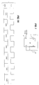
- Figure 1 is a block diagram of a master-slave flip flop.
- Figure 1A is a timing chart for Figure 1.
- Figure 2 is a block diagram of a flow through latch used in the present invention.
- Figure 2A is a timing chart for Figure 2.
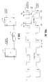
- Figure 3 is a logic diagram showing the clocking between master-slave flip flops.
- Figure 3A is a timing chart of the clock signal input to Figure 3.
- Figure 4 is a logic diagram showing the clocking between latches serving as master-slave flip flops according to an embodiment of the present invention.
- Figure 4A is a timing chart of the clock signal input to Figure 4.
- Figure 5 is an embodiment of a pulse generator used in the present invention.
- Figure 5A is a timing chart of the sliver pulses generated at the output of Figure 5.
- Figure 6 is a block diagram of an embodiment of the present invention showing multiple pulse generators on a VLSI chip.
- Master slave flip flop state devices will be referred to as flip flops, and simple flow through latch state devices will be described as latches.
- Flip flops generally contain two latches coupled together in a manner which allows a "race-free" operation between the latches. The output state of the flip flop changes on only one periodic clock edge.
- a race-free construction of a flip flop 5 is shown in Figure 1 and its operation is described by the timing charts of Figure 1A.
- the race-free operation means that the bi-stable element or state device output 6 may be used as the same state device's input 7.
- the output is a function of the previous state, and the output can therefore change at the arrival of a particular clock event 8, e.g., usually the rising edge of the clock signal. Note that the data changes only when the rising edge of the clock pulse occurs as seen in Fig. 1A.
- FIG 2 there is shown a simple latch 9 having the characteristic of allowing data 13 to flow through the latch 9 whenever the clock input 11 is in the "open" state.
- the latch 9 is held open when the clock signal 11 is high and the data 13 is latched when the clock signal 11 goes low.
- the operation of the typical flow through latch 9 is shown by the timing chart of Figure 2A. Note that a simple flow through latch 9 cannot be used to send data 13 back to itself (as in the flip flop example above), due to the data "racing" during the time period when the clock is held open. In this case, when the clock is open, the data circulates continuously independent of the clock signal.
- FIG. 3 there is shown a logic circuit including two master-slave flip flops 10 and 12 coupled by a delay 14.
- the Q output of input flip flop 10 is coupled through the delay 14 to the D input of destination flip flop 12.
- the arrangement illustrates the clocking of data through two typical master-slave flip flops.
- the flip flops 10 and 12 further include a source clock input 16 and a destination clock input 18, respectively.
- the clock inputs 16, 18 are from a single clock source and therefore have an approximately equal timing as shown in the timing chart of Figure 3.
- the maximum delay MAX DLY allowed between the two flip flops is less than or equal to the CYCLE time minus the clock skew S minus the "data to clock set up" time T su for the destination flip flop 12 minus the maximum propagation delay T pd (max) through the flip flop 10 as shown by Eq. (2).
- latches 30 and 32 coupled together via a delay DLY 34.
- the Q output of input latch 30 is coupled via the delay 34 to the D input of destination latch 32.
- the Q output of latch 32 is fed back through delay 40 into the D input of latch 30.
- a source clock signal 36 and a destination clock signal 38 are fed to the clock inputs of latches 30 and 32, respectively.
- the timing of the source clock signal 36 and the destination clock signal 38 is shown in Figure 4A. It is noted that for the flow through latches 30 and 32, the data is latched on the falling edge of the clock signal and the latch is opened on the rising edge of the clock signal.
- Each of the latches 30, 32 can be made to operate approximately as a flip flop as will be shown below.
- the minimum delay MIN DLY and maximum delay MAX DLY for the latch circuit operation is illustrated in Figure 4A and described in equations (3) and (4).
- the MIN DLY is greater than or equal to the width W of the clock pulse corresponding to the time the latch is open, plus the clock skew S plus the "clock to data hold" time T hld for the destination latch 32 minus the minimum propagation delay T pd (min) through the latch 30 as shown by Eq. (3).
- the MAX DLY is less than or equal to the CYCLE time minus the clock skew S minus the "clock to data set up" time T su for the destination latch 32 minus the maximum propagation delay T pd (max) through the latch 30 plus the width W of the clock pulse as shown by Eq. (4).
- Figure 5 shows a simple embodiment of a logic circuit for generating sliver pulses.
- a clock source 50 is coupled to the inputs of AND gate 54.
- a delay 52 is introduced between the clock source 50 and one input of the AND gate 54. This delay 52 can be a latch 52 having its clock input held open.
- the example of Figure 5 uses a 50% duty cycle from clock source 50 to the inputs of AND gate 54. Due to the delay, T pd (latch), introduced by the latch 52, a narrow sliver pulse having a width equalling T pd (latch) plus T pd (gate) is generated as shown in Figure 5A.
- the width of this sliver pulse can be made as narrow as physically possible. However, it is physically difficult to propagate such a narrow pulse in a VLSI design. The actual implementation should attempt to match the sliver width to the latch propagation delay T pd .
- the present invention utilizes the correlation factor with respect to circuit parameters on VLSI chips. Correlation is defined as how well two circuit parameters track each other. For example, if the two delays of two different state devices correlate 100%, then their respective delays would be identical. If the delays have 0% correlation, then there is no relationship whatsoever between them.
- the correlation factor takes into account the fact that the properties, e.g., T pd (min and max), power consumption, etc. of state devices similarly situated on a VLSI chip correspond closely with other state devices spaced nearby. This correlation is due to several factors, e.g., similar processing of the chip and the similar nature of the material, i.e., the silicon parameters of areas on the chip do not vary much with those areas in close spatial proximity.
- correlative properties are taken advantage of by creating pulse generators on the VLSI design using state devices which are nearby the state devices to be clocked. Because of this, sliver pulses can be generated which have a width substantially identical to the propagation delay T pd of closely spaced state devices.
- FIG. 6 shows an example of how the correlated sliver latches can be implemented on a VLSI design chip 58.
- the chip 58 includes blocks 60, 62 and 64 of physically similar latches L on the chip 58. Further, each block 60, 62, and 64 includes a pulse or sliver generator G formed by using one of the latches L.
- a clock signal CLK is input to the chip 58 at pin 56 and propagates to a distribution stage 59.
- the distribution stage 59 splits the clock signal into several signals and propagates each clock signal to one of the blocks 60, 62, and 64.
- the sliver generator G generates the narrow sliver pulses to operate the latches L in each of the blocks.
- sliver latches consumes two units of power and occupies two units of area; and a latch consumes one unit of power and occupies one unit of area; a sliver generator consumes one unit of power and occupies one unit of area. It is possible that sliver latches be grouped in clusters of four, six or eight, with each cluster containing a single pulse generator. It is noted, however, that the actual group size is an arbitrary figure.
- a cluster of four latches and one sliver generator may serve as four master-slave flip flops while consuming only five units of area, i.e., five "cells".
- each flip flop requires two latches thus consuming two units of area
- a pure flip flop design requires eight units of area to produce four master-slave flip flops. Therefore, there is a fractional reduction of "3/8ths" in the number of cells saved using a sliver latch design.
- sliver latches Assuming a particular VLSI design having a total usable area of 3,000 cells, but with only 700 flip flops, then the power and cell savings achieved by using sliver latches can be determined.
- the sliver latches are assumed to be available in clusters of four only.
- the power saved can then be computed by determining the "cells saved ratio", since both the cell area and power proportions are the same.
Landscapes
- Manipulation Of Pulses (AREA)
- Pulse Circuits (AREA)
- Logic Circuits (AREA)
- Tests Of Electronic Circuits (AREA)
Claims (4)
- VLSI-Schaltung, mit:die Impulsgeneratorschaltung (G) enthält:a) mehreren physikalisch ähnlichen Durchlauf-Zwischenspeichern (L) auf einem VLSI-Chip, wobei jeder der Durchlauf-Zwischenspeicher (L) einen Eingang, einen Ausgang und einen Takteingang besitzt; undb) wenigstens einer Impulsgeneratorschaltung (G) zum Erzeugen verschmälerter Impulse, die mit den Takteingängen der Durchlauf-Zwischenspeicher (L) gekoppelt ist, wobeii) ein Verzögerungselement (52), das aus einem Durchlauf-Zwischenspeicher besteht, der den zu taktenden Zwischenspeichern (L) physikalisch ähnlich ist und dessen Takteingang offengehalten wird,ii) ein Gatter (54), das an den Ausgang des Verzögerungselements (52) angeschlossen ist, undiii) eine Taktquelle (50), die mit dem Verzögerungselement (52) und mit dem Gatter (54) gekoppelt ist, um die verschmälerten Impulse zu erzeugen, die in die mehreren Durchlauf-Zwischenspeicher (L) eingegeben werden,iv) wobei der das Verzögerungselement (52) enthaltende Impulsgenerator (G) auf der VLSI-Schaltung sehr nahe bei den Durchlauf-Zwischenspeichern (L) angeordnet ist.
- VLSI-Schaltung nach Anspruch 1, bei der eine Impulsgeneratorschaltung (G) für vier der mehreren zu taktenden Durchlauf-Zwischenspeicher (L) vorgesehen ist.
- VLSI-Schaltung nach Anspruch 1, bei der eine Impulsgeneratorschaltung (G) für sechs der mehreren zu taktenden Durchlauf-Zwischenspeicher (L) vorgesehen ist.
- VLSI-Schaltung nach Anspruch 1, bei der eine Impulsgeneratorschaltung (G) für acht der mehreren zu taktenden Durchlauf-Zwischenspeicher (L) vorgesehen ist.
Applications Claiming Priority (2)
| Application Number | Priority Date | Filing Date | Title |
|---|---|---|---|
| US07/363,708 US5072132A (en) | 1989-06-09 | 1989-06-09 | Vsli latch system and sliver pulse generator with high correlation factor |
| US363708 | 1989-06-09 |
Publications (3)
| Publication Number | Publication Date |
|---|---|
| EP0401865A2 EP0401865A2 (de) | 1990-12-12 |
| EP0401865A3 EP0401865A3 (de) | 1993-07-07 |
| EP0401865B1 true EP0401865B1 (de) | 1999-01-27 |
Family
ID=23431370
Family Applications (1)
| Application Number | Title | Priority Date | Filing Date |
|---|---|---|---|
| EP90111017A Expired - Lifetime EP0401865B1 (de) | 1989-06-09 | 1990-06-11 | VLSI Schaltung mit von einem benachbarten angepassten Taktgenerator gesteuerten Verriegelungsschaltungen |
Country Status (7)
| Country | Link |
|---|---|
| US (1) | US5072132A (de) |
| EP (1) | EP0401865B1 (de) |
| JP (1) | JP2579237B2 (de) |
| KR (1) | KR930008418B1 (de) |
| AU (1) | AU631428B2 (de) |
| CA (1) | CA2017707A1 (de) |
| DE (1) | DE69032915T2 (de) |
Families Citing this family (14)
| Publication number | Priority date | Publication date | Assignee | Title |
|---|---|---|---|---|
| US5303350A (en) * | 1990-12-20 | 1994-04-12 | Acer Incorporated | Circuit for initializing registers using two input signals for writing default value into D-latch after a reset operation |
| US5175515A (en) * | 1991-06-21 | 1992-12-29 | Compaq Computer Corporation | Signal routing technique for electronic systems |
| US5552737A (en) * | 1994-07-11 | 1996-09-03 | International Business Machines Corporation | Scannable master slave latch actuated by single phase clock |
| US5642068A (en) * | 1994-08-08 | 1997-06-24 | Mosaid Technologies Incorporated | Clock period dependent pulse generator |
| US6115836A (en) * | 1997-09-17 | 2000-09-05 | Cypress Semiconductor Corporation | Scan path circuitry for programming a variable clock pulse width |
| US6229750B1 (en) | 1999-09-30 | 2001-05-08 | International Business Machines Corporation | Method and system for reducing power dissipation in a semiconductor storage device |
| US6609228B1 (en) | 2000-11-15 | 2003-08-19 | International Business Machines Corporation | Latch clustering for power optimization |
| US6621302B2 (en) | 2001-03-21 | 2003-09-16 | Bae Systems Information And Electronic Systems Integration, Inc | Efficient sequential circuits using critical race control |
| US7634749B1 (en) * | 2005-04-01 | 2009-12-15 | Cadence Design Systems, Inc. | Skew insensitive clocking method and apparatus |
| US7694242B1 (en) * | 2006-12-11 | 2010-04-06 | Cadence Design Systems, Inc. | System and method of replacing flip-flops with pulsed latches in circuit designs |
| US7746137B2 (en) | 2007-08-28 | 2010-06-29 | Qualcomm Incorporated | Sequential circuit element including a single clocked transistor |
| US7724058B2 (en) * | 2007-10-31 | 2010-05-25 | Qualcomm Incorporated | Latch structure and self-adjusting pulse generator using the latch |
| US9564881B2 (en) | 2015-05-22 | 2017-02-07 | Qualcomm Incorporated | Area-efficient metal-programmable pulse latch design |
| US9979394B2 (en) | 2016-02-16 | 2018-05-22 | Qualcomm Incorporated | Pulse-generator |
Citations (2)
| Publication number | Priority date | Publication date | Assignee | Title |
|---|---|---|---|---|
| JPS59104820A (ja) * | 1982-12-08 | 1984-06-16 | Hitachi Ltd | フリツプフロツプ回路 |
| EP0304930A2 (de) * | 1987-08-27 | 1989-03-01 | Kabushiki Kaisha Toshiba | Integrierte Halbleiterschaltung mit Signallinien |
Family Cites Families (14)
| Publication number | Priority date | Publication date | Assignee | Title |
|---|---|---|---|---|
| JPS57112129A (en) * | 1980-12-27 | 1982-07-13 | Yamatake Honeywell Co Ltd | Latch circuit |
| JPS585022A (ja) * | 1981-07-02 | 1983-01-12 | Nec Corp | 前縁微分回路 |
| US4425514A (en) * | 1981-11-10 | 1984-01-10 | Rca Corporation | Fixed pulse width, fast recovery one-shot pulse generator |
| US4570082A (en) * | 1983-11-25 | 1986-02-11 | International Business Machines Corporation | Single clocked latch circuit |
| FR2556903B1 (fr) * | 1983-12-15 | 1986-04-11 | Telediffusion Fse | Procede et circuits de regeneration d'instants significatifs d'un signal periodique |
| JPS60261211A (ja) * | 1984-06-08 | 1985-12-24 | Nec Corp | マスタ−・スレ−ブ型フリツプ・フロツプ |
| JPH0630377B2 (ja) * | 1984-06-15 | 1994-04-20 | 株式会社日立製作所 | 半導体集積回路装置 |
| US4701860A (en) * | 1985-03-07 | 1987-10-20 | Harris Corporation | Integrated circuit architecture formed of parametric macro-cells |
| US4733111A (en) * | 1985-07-17 | 1988-03-22 | CSELT--Centro Studi e Laboratori Telecomunicazioni S.p.A. | Sequential-logic basic element in CMOS technology operating by a single clock signal |
| CA1275310C (en) * | 1985-11-26 | 1990-10-16 | Katuhisa Kubota | Master slave latch circuit |
| US4797575A (en) * | 1986-12-05 | 1989-01-10 | Western Digital Corporation | Flip-flop with identical propagation delay in clock pass through mode and in normal operation |
| US4786829A (en) * | 1987-02-24 | 1988-11-22 | Letcher John H | Latched fedback memory finite-state-engine |
| JPS6460015A (en) * | 1987-08-31 | 1989-03-07 | Fujitsu Ltd | Flip flop circuit |
| US4864161A (en) * | 1988-05-05 | 1989-09-05 | Altera Corporation | Multifunction flip-flop-type circuit |
-
1989
- 1989-06-09 US US07/363,708 patent/US5072132A/en not_active Expired - Lifetime
-
1990
- 1990-05-25 AU AU55963/90A patent/AU631428B2/en not_active Ceased
- 1990-05-29 JP JP2139524A patent/JP2579237B2/ja not_active Expired - Lifetime
- 1990-05-29 CA CA002017707A patent/CA2017707A1/en not_active Abandoned
- 1990-06-07 KR KR1019900008309A patent/KR930008418B1/ko not_active Expired - Fee Related
- 1990-06-11 DE DE69032915T patent/DE69032915T2/de not_active Expired - Fee Related
- 1990-06-11 EP EP90111017A patent/EP0401865B1/de not_active Expired - Lifetime
Patent Citations (2)
| Publication number | Priority date | Publication date | Assignee | Title |
|---|---|---|---|---|
| JPS59104820A (ja) * | 1982-12-08 | 1984-06-16 | Hitachi Ltd | フリツプフロツプ回路 |
| EP0304930A2 (de) * | 1987-08-27 | 1989-03-01 | Kabushiki Kaisha Toshiba | Integrierte Halbleiterschaltung mit Signallinien |
Non-Patent Citations (2)
| Title |
|---|
| M.STANSBERRY: 'Projektstudien für CMOS-Gate-Arrays', ELEKTRONIK, 21-03-1986, no. 6, pages 116-121 * |
| U.TIETZE et al.: 'Halbleiter-Schaltungstechnik', 1985, Berlin, DE; pages 215, 232, 235-237 * |
Also Published As
| Publication number | Publication date |
|---|---|
| DE69032915T2 (de) | 1999-09-16 |
| DE69032915D1 (de) | 1999-03-11 |
| KR910001964A (ko) | 1991-01-31 |
| US5072132A (en) | 1991-12-10 |
| CA2017707A1 (en) | 1990-12-09 |
| EP0401865A2 (de) | 1990-12-12 |
| JPH0326104A (ja) | 1991-02-04 |
| JP2579237B2 (ja) | 1997-02-05 |
| AU5596390A (en) | 1990-12-13 |
| KR930008418B1 (ko) | 1993-08-31 |
| AU631428B2 (en) | 1992-11-26 |
| EP0401865A3 (de) | 1993-07-07 |
Similar Documents
| Publication | Publication Date | Title |
|---|---|---|
| EP0401865B1 (de) | VLSI Schaltung mit von einem benachbarten angepassten Taktgenerator gesteuerten Verriegelungsschaltungen | |
| US6608513B2 (en) | Flip-flop circuit having dual-edge triggered pulse generator | |
| US6345328B1 (en) | Gear box for multiple clock domains | |
| KR101089153B1 (ko) | 상이한 클록 도메인 간에서의 데이터 신호 전송 방법 및 집적 회로 | |
| EP3465911B1 (de) | Datenangesteuerter flipflop mit niedrigem clock power | |
| US5896052A (en) | Methods to avoid instability | |
| US6064247A (en) | Multiple frequency clock generation and synchronization | |
| JPH10117185A (ja) | データを転送するためのシンクロナイザ、方法及びシステム | |
| US6172540B1 (en) | Apparatus for fast logic transfer of data across asynchronous clock domains | |
| EP1434122A2 (de) | Vorrichtung und Verfahren zur Wiederherstellung von Zurücksetz- und Taktsignalen sowie ein schnelles digitales System mit einer solche Vorrichtung. | |
| US6208703B1 (en) | First-in-first-out synchronizer | |
| US6507230B1 (en) | Clock generator having a deskewer | |
| US6982575B2 (en) | Clock ratio data synchronizer | |
| US6188262B1 (en) | Synchronous polyphase clock distribution system | |
| US6304125B1 (en) | Method for generating and distribution of polyphase clock signals | |
| CN109687860B (zh) | 一种多相时钟串行器及信号转换系统 | |
| US6633995B1 (en) | System for generating N pipeline control signals by delaying at least one control signal corresponding to a subsequent data path circuit | |
| JPH09167134A (ja) | データ同期システム | |
| US6026141A (en) | One load conditional look ahead counter | |
| GB2326258A (en) | Clock signal modelling circuit | |
| EP0511423A1 (de) | Elektrischer Schaltkreis zum Generieren von Impulsreihen | |
| KR100321732B1 (ko) | 디지털 링 동기식 미러 딜레이를 이용한 지연고정루프 | |
| WO2009136875A1 (en) | Synchronous sequential logic device using double triggered flip-flops and method for skewed triggering such state storing registers | |
| US6831482B2 (en) | Control of guard-flops | |
| KR19990008193A (ko) | 지연-정합된 클럭과 데이터신호의 발생기 |
Legal Events
| Date | Code | Title | Description |
|---|---|---|---|
| PUAI | Public reference made under article 153(3) epc to a published international application that has entered the european phase |
Free format text: ORIGINAL CODE: 0009012 |
|
| 17P | Request for examination filed |
Effective date: 19900711 |
|
| AK | Designated contracting states |
Kind code of ref document: A2 Designated state(s): DE FR GB IT NL |
|
| PUAL | Search report despatched |
Free format text: ORIGINAL CODE: 0009013 |
|
| AK | Designated contracting states |
Kind code of ref document: A3 Designated state(s): DE FR GB IT NL |
|
| 17Q | First examination report despatched |
Effective date: 19950328 |
|
| APAB | Appeal dossier modified |
Free format text: ORIGINAL CODE: EPIDOS NOAPE |
|
| APAD | Appeal reference recorded |
Free format text: ORIGINAL CODE: EPIDOS REFNE |
|
| APAB | Appeal dossier modified |
Free format text: ORIGINAL CODE: EPIDOS NOAPE |
|
| GRAG | Despatch of communication of intention to grant |
Free format text: ORIGINAL CODE: EPIDOS AGRA |
|
| GRAH | Despatch of communication of intention to grant a patent |
Free format text: ORIGINAL CODE: EPIDOS IGRA |
|
| GRAH | Despatch of communication of intention to grant a patent |
Free format text: ORIGINAL CODE: EPIDOS IGRA |
|
| GRAA | (expected) grant |
Free format text: ORIGINAL CODE: 0009210 |
|
| AK | Designated contracting states |
Kind code of ref document: B1 Designated state(s): DE FR GB IT NL |
|
| PG25 | Lapsed in a contracting state [announced via postgrant information from national office to epo] |
Ref country code: FR Free format text: THE PATENT HAS BEEN ANNULLED BY A DECISION OF A NATIONAL AUTHORITY Effective date: 19990127 |
|
| REF | Corresponds to: |
Ref document number: 69032915 Country of ref document: DE Date of ref document: 19990311 |
|
| ITF | It: translation for a ep patent filed | ||
| ET | Fr: translation filed | ||
| PG25 | Lapsed in a contracting state [announced via postgrant information from national office to epo] |
Ref country code: GB Free format text: LAPSE BECAUSE OF NON-PAYMENT OF DUE FEES Effective date: 19990611 |
|
| PLBE | No opposition filed within time limit |
Free format text: ORIGINAL CODE: 0009261 |
|
| STAA | Information on the status of an ep patent application or granted ep patent |
Free format text: STATUS: NO OPPOSITION FILED WITHIN TIME LIMIT |
|
| PG25 | Lapsed in a contracting state [announced via postgrant information from national office to epo] |
Ref country code: NL Free format text: LAPSE BECAUSE OF NON-PAYMENT OF DUE FEES Effective date: 20000101 |
|
| 26N | No opposition filed | ||
| GBPC | Gb: european patent ceased through non-payment of renewal fee |
Effective date: 19990611 |
|
| NLV4 | Nl: lapsed or anulled due to non-payment of the annual fee |
Effective date: 20000101 |
|
| PG25 | Lapsed in a contracting state [announced via postgrant information from national office to epo] |
Ref country code: DE Free format text: LAPSE BECAUSE OF NON-PAYMENT OF DUE FEES Effective date: 20000503 |
|
| REG | Reference to a national code |
Ref country code: FR Ref legal event code: ST |
|
| PG25 | Lapsed in a contracting state [announced via postgrant information from national office to epo] |
Ref country code: IT Free format text: LAPSE BECAUSE OF NON-PAYMENT OF DUE FEES Effective date: 20050611 |
|
| APAH | Appeal reference modified |
Free format text: ORIGINAL CODE: EPIDOSCREFNO |