EP0304930A2 - Integrierte Halbleiterschaltung mit Signallinien - Google Patents
Integrierte Halbleiterschaltung mit Signallinien Download PDFInfo
- Publication number
- EP0304930A2 EP0304930A2 EP88113947A EP88113947A EP0304930A2 EP 0304930 A2 EP0304930 A2 EP 0304930A2 EP 88113947 A EP88113947 A EP 88113947A EP 88113947 A EP88113947 A EP 88113947A EP 0304930 A2 EP0304930 A2 EP 0304930A2
- Authority
- EP
- European Patent Office
- Prior art keywords
- cell
- signal
- connection
- line
- connection line
- Prior art date
- Legal status (The legal status is an assumption and is not a legal conclusion. Google has not performed a legal analysis and makes no representation as to the accuracy of the status listed.)
- Granted
Links
Images


Classifications
-
- H—ELECTRICITY
- H10—SEMICONDUCTOR DEVICES; ELECTRIC SOLID-STATE DEVICES NOT OTHERWISE PROVIDED FOR
- H10W—GENERIC PACKAGES, INTERCONNECTIONS, CONNECTORS OR OTHER CONSTRUCTIONAL DETAILS OF DEVICES COVERED BY CLASS H10
- H10W20/00—Interconnections in chips, wafers or substrates
- H10W20/40—Interconnections external to wafers or substrates, e.g. back-end-of-line [BEOL] metallisations or vias connecting to gate electrodes
- H10W20/41—Interconnections external to wafers or substrates, e.g. back-end-of-line [BEOL] metallisations or vias connecting to gate electrodes characterised by their conductive parts
- H10W20/43—Layouts of interconnections
Definitions
- the present invention relates to a semicustom semiconductor IC (integrated circuit) device and, in particular, to a semiconductor IC device having signal lines for supplying a signal, such as a clock signal, to any places of an associated circuit.
- Fig. 1 is a plan view showing a pattern of a conventional standard cell-or gate array-type semiconductor IC device.
- reference numeral 50 shows an IC chip body including a plurality of cell rows 51 each constituted by a plurality of standard cells and macroblock 52, such as a memory.
- a plurality of I/O cells 53 are provided around chip body 50.
- cell 53A is of a clock driver type which has a greater drive capability and receives a clock signal.
- the clock signal is amplified at cell 53A and supplied via signal lines 54 to an associated cell in respective cell row 51.
- Fig. 2 is an equivalent circuit showing a relation of a signal connection between the clock driver cell and the standard cells in the respective cell row.
- reference numerals 55 show standard cells, such as flip-flops (F/F), which are arranged in the respective cell rows and need an associated clock signal.
- connection layout of signal lines 54 for supplying a clock signal is implemented by randomly finding unconnected areas by virtue of a layout CAD, resulting in the connection line being excessively longer. For this reason, the associated signal lines have a resistance too great to be disregarded and a signal is supplied to the respective cell with a different delay time.
- an output waveform from the clock driver cell is distorted, sometimes prominently, depending upon the distance from the clock driver cell to the respective associated cell. If that signal is a clock signal, the integrated circuit involves a problem, such as a clock skew, thus failing to perform a normal operation. This problem cannot be resolved with the use of a clock driver cell of a greater driving capability, because it is caused by the resistance of the signal line per se. That is to say, in the conventional device, the connection length of the signal line becomes excessively longer and the signal is supplied to the associated cells with a different delay time and hence with a different phase. Furthermore, the signal waveform becomes distorted prominently at the far end cell or cells.
- a semiconductor integrated circuit device which comprises: a plurality of cell rows each having a plurality of standard cells; signal connection cells provided at the respective cell row in a manner to be located on a single straight line; a connection line for cell rows which is connected to the signal connection cells and adapted to supply a signal which is propagated via the signal connection cell to the associated cell in the corresponding cell row; and a cell-to-cell connection line connecting the signal connection cells together and having a broader connection width than that of an ordinary connection line.
- the signal connection cells are connected together by the cell-to-cell connection line whose connection width is broader than that of the ordinary connection line, resulting in a signal being propagated to the associated cell in a low-resistance fashion.
- the signal connection cells are arranged at the respective cell rows so as to be located on a single straight line and it is, therefore, possible to connect the respective signal connection cells together by the cell-to-cell connection line so that a distance of the signal connection line can be reduced.
- a signal coming from the signal connection cell is supplied in a row unit to the associated cell in the respective cell row via the line for cell rows, so that a signal is propagated over a minimum connection line length.
- a semiconductor integrated circuit device which can reduce a signal connection line length and achieve a low-resistance feature so that the phase shift of a signal waveform, as well as the deformation of the signal waveform at an output of the cell to which it is supplied from a clock driver cell, occurs.
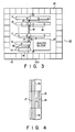
- Fig. 3 is a plan view showing an IC chip pattern obtained by incorporating an invention into a standard cell type integrated circuit.
- IC chip body 10 includes a plurality of cell rows 11 each having a plurality of cells and macro block 12, such as a memory.
- signal connection cells 13 are each so provided as to be located on a single line across the cell row array.
- These signal connection cells 13 are mutually connected by cell-to-cell connection line 14 whose width is broader than that of those ordinary lines in the respective cell rows.
- I/O cell 15A is a clock driver cell of a greater driving capability which receives a clock signal.
- the clock signal is amplified by clock driver cell 15A and coupled via a corresponding signal line to signal connection cell 13 at a location nearest to cell 15A.
- Connection line 16 for cell rows which has a width equal to that of the ordinary connection line is connected to signal connection cell 13.
- the clock signal is supplied to a clock signal demand standard cell, such as a standard flip-flop cell.
- Fig. 4 is a plan view showing a detailed pattern of signal connection cell 13 in the aforementioned integrated circuit.
- Signal connection cell 13 has a metal connection layer, such as aluminum as well as input-side connection line 17 equal in width to connection line 14 and output-side connection line 18 connected to input-side connection line 17 and having a width equal to that of the ordinary connection line.
- Input side connection line 17 is connection to cell-to-cell connection line 14 and output side connection line 18 is connected to cell row connection line 16, not shown in Fig. 4.
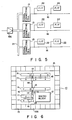
- Fig. 5 is an equivalent circuit showing a relation of signal connection lines between the clock driver cell and standard cells in the respective cell row.
- connection line 21 indicated by a broad line comprises input-side connection line 17 and cell-to-cell connection line 14 both having a corresponding connection line in signal connection cell 13.
- a clock signal is propagated from clock driver cell 15A via connection line 21 to the cell row position.
- Connection line 21 has a greater width and extends on a straight line as shown in Fig. 3 so as to obtain a minimum connection line. It is thus possible to obtain an adequately small resistive value. As a result, the delay times for a signal to reach the respective cell rows become adequately small and equal to each other.
- a clock signal is supplied from respective connection cell 13 to a clock signal demand standard cell, such as a flip-flop (F/F) cell, in the respective row via connection line 16 for the corresponding cell row. It is thus possible to provide a minimum connection line length for connection line 16 with the ordinary connection line of the aforementioned width, and to solve, for example, a "clock skew" problem.
- a clock signal demand standard cell such as a flip-flop (F/F) cell
- Fig. 6 is a plan view showing an IC chip pattern when the semiconductor IC device of the present invention is applied to a standard cell type integrated circuit.
- connection line 16 for cell rows is shared between two respective adjacent cell rows, thus allowing the reduction of the length of a connection line for propagating a clock signal so that the clock signal can drive the corresponding cell without loosing an enhanced drive capability.
- Fig. 7 is a plan view showing a cell configuration pattern for signal connection when a semiconductor device of the present invention is applied to a standard cell type integrated circuit.
- cell 33 for signal connection includes input-side connection line 37 and output-side connection line 38 both made of a metal connection line, such as aluminum, and amplifier 39 connected between input-side connection line 37 and output-side connection line 38.
- a cell-to-cell connection line is of two type: connection line 34A and connection line 34B.
- Input-side connection line 37 in the signal connection cell is connected to cell-to-cell connection line 34A of a broader connection width than that of the ordinary connection line and to cell-to-cell connection line 34 whose width is equal to that of the ordinary connection line.
- Output-side connection line 38 in the signal connection cell is connected to connection line 16, not shown in Fig. 7, for cell rows.
- Fig. 8 is a plan view showing an IC chip configuration pattern with signal connection cells shown in Fig. 7 incorporated therein.
- amplifier 39 is connected between input-side connection line 37 and output-side connection line 38 in respective signal connection cell 33 so that a clock signal is supplied to the respective cell row with an enhanced cell drive capability.
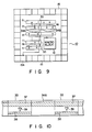
- Fig. 9 is a plan view showing an IC chip configuration pattern in a semiconductor IC device, with the signal connection cells (Fig. 7) incorporated therein, according to another embodiment of the present invention.
- connection line 16 for cell rows is provided for every two adjacent cells as in the embodiment shown in Fig. 6. According to the present invention, it is possible to reduce the length of a connection line for propagating a clock signal and hence to provide an enhanced cell drive capability with which a clock signal is propagated to the associated cell.
- Fig. 10 is a plan view showing a connection cell configuration pattern for signal connection in a semiconductor IC device, with a standard cell type integrated circuit incorporated therein, according to another embodiment of the present invention.
- signal connection cells 33 include input-side connection line 37, output-side connection line 38 and amplifier 39 as in Fig. 7.
- the cell-to-cell connection line is constituted by one type of connection line 34A whose width is greater than that of the ordinary connection line. Only input-side connection line 37 in the signal connection cell is connected to each other via cell-to-cell connection line 34A. This type of the integrated circuit is advantageous in the case where the number of clock signal demand cells in the respective cell row is averaged.
- the present invention is not restricted to the aforementioned embodiment and can be changed in a variety of ways without being restricted to the aforementioned embodiments.
- a clock signal has been explained as being supplied or propagated via the signal connection cell, the present invention can also been reduced to practice if an ordinary signal is used in place of the clock signal.
Landscapes
- Design And Manufacture Of Integrated Circuits (AREA)
- Semiconductor Integrated Circuits (AREA)
Applications Claiming Priority (2)
| Application Number | Priority Date | Filing Date | Title |
|---|---|---|---|
| JP213545/87 | 1987-08-27 | ||
| JP62213545A JPH0828421B2 (ja) | 1987-08-27 | 1987-08-27 | 半導体集積回路装置 |
Publications (3)
| Publication Number | Publication Date |
|---|---|
| EP0304930A2 true EP0304930A2 (de) | 1989-03-01 |
| EP0304930A3 EP0304930A3 (en) | 1989-04-05 |
| EP0304930B1 EP0304930B1 (de) | 1993-03-31 |
Family
ID=16640970
Family Applications (1)
| Application Number | Title | Priority Date | Filing Date |
|---|---|---|---|
| EP88113947A Expired - Lifetime EP0304930B1 (de) | 1987-08-27 | 1988-08-26 | Integrierte Halbleiterschaltung mit Signallinien |
Country Status (4)
| Country | Link |
|---|---|
| US (1) | US4883980A (de) |
| EP (1) | EP0304930B1 (de) |
| JP (1) | JPH0828421B2 (de) |
| DE (1) | DE3879813T2 (de) |
Cited By (4)
| Publication number | Priority date | Publication date | Assignee | Title |
|---|---|---|---|---|
| US5304826A (en) * | 1989-09-22 | 1994-04-19 | Kabushiki Kaisha Toshiba | Semiconductor integrated circuit device |
| EP0401865B1 (de) * | 1989-06-09 | 1999-01-27 | Digital Equipment Corporation | VLSI Schaltung mit von einem benachbarten angepassten Taktgenerator gesteuerten Verriegelungsschaltungen |
| EP0791930A3 (de) * | 1995-10-02 | 1999-05-26 | Matsushita Electronics Corporation | Elektrische Signalversorgungsschaltung und Halbleiterspeicheranordnung |
| SG87731A1 (en) * | 1989-09-08 | 2002-04-16 | Seiko Epson Corp | Master slice integrated circuit device |
Families Citing this family (15)
| Publication number | Priority date | Publication date | Assignee | Title |
|---|---|---|---|---|
| JPH0229124A (ja) * | 1988-07-19 | 1990-01-31 | Toshiba Corp | スタンダードセル |
| JPH02106968A (ja) * | 1988-10-17 | 1990-04-19 | Hitachi Ltd | 半導体集積回路装置及びその形成方法 |
| US5291043A (en) * | 1990-02-07 | 1994-03-01 | Mitsubishi Denki Kabushiki Kaisha | Semiconductor integrated circuit device having gate array |
| JP2545626B2 (ja) * | 1990-02-07 | 1996-10-23 | 三菱電機株式会社 | ゲートアレイ |
| JPH03278449A (ja) * | 1990-03-02 | 1991-12-10 | Matsushita Electron Corp | 半導体集積回路の自動配線方法 |
| JPH04116951A (ja) * | 1990-09-07 | 1992-04-17 | Fujitsu Ltd | 半導体集積回路 |
| KR930008310B1 (ko) * | 1991-02-05 | 1993-08-27 | 삼성전자 주식회사 | 반도체 메모리장치의 워드라인드라이버단 배치방법 |
| JP2917604B2 (ja) * | 1991-08-30 | 1999-07-12 | 日本電気株式会社 | 半導体集積回路のレイアウト設計方法 |
| KR940008722B1 (ko) * | 1991-12-04 | 1994-09-26 | 삼성전자 주식회사 | 반도체 메모리 장치의 워드라인 드라이버 배열방법 |
| JP3178932B2 (ja) * | 1993-03-02 | 2001-06-25 | 富士通株式会社 | 半導体集積回路装置 |
| EP0650194B1 (de) * | 1993-10-21 | 1999-11-10 | Advanced Micro Devices, Inc. | Dynamischer Bus von hoher Dichte |
| JPH10246754A (ja) * | 1997-03-03 | 1998-09-14 | Mitsubishi Electric Corp | クロックドライバ回路及び半導体集積回路装置 |
| JP4025044B2 (ja) * | 2001-09-27 | 2007-12-19 | 株式会社東芝 | 半導体集積回路装置 |
| US7628452B2 (en) * | 2008-02-29 | 2009-12-08 | Shanghai Industries Group, Ltd. | Rocker base |
| CN110824181B (zh) * | 2019-10-18 | 2021-10-15 | 中国航空工业集团公司西安飞行自动控制研究所 | 一种低电阻敏感器件信号连接方法 |
Family Cites Families (7)
| Publication number | Priority date | Publication date | Assignee | Title |
|---|---|---|---|---|
| US3818289A (en) * | 1972-04-10 | 1974-06-18 | Raytheon Co | Semiconductor integrated circuit structures |
| JPS5835963A (ja) * | 1981-08-28 | 1983-03-02 | Fujitsu Ltd | 集積回路装置 |
| JPS59182540A (ja) * | 1983-04-01 | 1984-10-17 | Hitachi Ltd | 半導体装置における配線パタ−ンの設計方法 |
| US4575745A (en) * | 1983-06-21 | 1986-03-11 | Rca Corporation | Tailorable standard cells and method for tailoring the performance of IC designs |
| JPH0630377B2 (ja) * | 1984-06-15 | 1994-04-20 | 株式会社日立製作所 | 半導体集積回路装置 |
| JPS62140430A (ja) * | 1985-12-16 | 1987-06-24 | Toshiba Corp | 半導体集積回路の配線方法 |
| JPS62141737A (ja) * | 1985-12-16 | 1987-06-25 | Matsushita Electric Ind Co Ltd | セルの配置方法 |
-
1987
- 1987-08-27 JP JP62213545A patent/JPH0828421B2/ja not_active Expired - Fee Related
-
1988
- 1988-08-26 US US07/238,229 patent/US4883980A/en not_active Expired - Lifetime
- 1988-08-26 EP EP88113947A patent/EP0304930B1/de not_active Expired - Lifetime
- 1988-08-26 DE DE88113947T patent/DE3879813T2/de not_active Expired - Fee Related
Cited By (4)
| Publication number | Priority date | Publication date | Assignee | Title |
|---|---|---|---|---|
| EP0401865B1 (de) * | 1989-06-09 | 1999-01-27 | Digital Equipment Corporation | VLSI Schaltung mit von einem benachbarten angepassten Taktgenerator gesteuerten Verriegelungsschaltungen |
| SG87731A1 (en) * | 1989-09-08 | 2002-04-16 | Seiko Epson Corp | Master slice integrated circuit device |
| US5304826A (en) * | 1989-09-22 | 1994-04-19 | Kabushiki Kaisha Toshiba | Semiconductor integrated circuit device |
| EP0791930A3 (de) * | 1995-10-02 | 1999-05-26 | Matsushita Electronics Corporation | Elektrische Signalversorgungsschaltung und Halbleiterspeicheranordnung |
Also Published As
| Publication number | Publication date |
|---|---|
| JPH0828421B2 (ja) | 1996-03-21 |
| US4883980B1 (de) | 1993-02-23 |
| DE3879813D1 (de) | 1993-05-06 |
| US4883980A (en) | 1989-11-28 |
| EP0304930A3 (en) | 1989-04-05 |
| EP0304930B1 (de) | 1993-03-31 |
| DE3879813T2 (de) | 1993-10-07 |
| JPS6455841A (en) | 1989-03-02 |
Similar Documents
| Publication | Publication Date | Title |
|---|---|---|
| EP0304930A2 (de) | Integrierte Halbleiterschaltung mit Signallinien | |
| US4811073A (en) | Gate array arrangement | |
| EP0181059B1 (de) | Integrierte Halbleiterschaltung für Taktimpulsverteilung | |
| EP0133958B1 (de) | "Master-Slice"-Halbleiteranordnung | |
| US5923060A (en) | Reduced area gate array cell design based on shifted placement of alternate rows of cells | |
| US5422441A (en) | Master slice integrated circuit having a reduced chip size and a reduced power supply noise | |
| US6037820A (en) | Clock distribution circuit in a semiconductor integrated circuit | |
| US4947233A (en) | Semi-custom LSI having input/output cells | |
| US5270592A (en) | Clock supply circuit layout in a circuit area | |
| US6066866A (en) | Semiconductor device with alternating general-purpose functional regions and specific functional regions | |
| US4930000A (en) | Terminal assembly for an integrated semiconductor circuit | |
| EP0416456B1 (de) | Stromversorgungssystem für Master slice integrierte Schaltung | |
| US5401988A (en) | Standard cell layout arrangement for an LSI circuit | |
| US5835505A (en) | Semiconductor integrated circuit and system incorporating the same | |
| JPS60134462A (ja) | 集積化半導体論理回路装置 | |
| JP3017181B1 (ja) | 半導体集積回路の配線方法 | |
| US20010008379A1 (en) | Programmable integrated circuit device | |
| JP2508206B2 (ja) | 集積回路装置 | |
| JPH05251671A (ja) | ゲートアレイ方式の半導体集積回路装置 | |
| JPH0560666B2 (de) | ||
| US6621171B2 (en) | Semiconductor device having a wire laid between pads | |
| JPS5963743A (ja) | 半導体集積回路装置 | |
| EP0418912A2 (de) | Integrierte Halbleiterschaltungsanordnung | |
| JPH04258164A (ja) | マスタースライス方式半導体集積回路 | |
| JPH04324956A (ja) | 半導体装置 |
Legal Events
| Date | Code | Title | Description |
|---|---|---|---|
| PUAI | Public reference made under article 153(3) epc to a published international application that has entered the european phase |
Free format text: ORIGINAL CODE: 0009012 |
|
| PUAL | Search report despatched |
Free format text: ORIGINAL CODE: 0009013 |
|
| 17P | Request for examination filed |
Effective date: 19880831 |
|
| AK | Designated contracting states |
Kind code of ref document: A2 Designated state(s): DE FR GB |
|
| AK | Designated contracting states |
Kind code of ref document: A3 Designated state(s): DE FR GB |
|
| 17Q | First examination report despatched |
Effective date: 19901120 |
|
| GRAA | (expected) grant |
Free format text: ORIGINAL CODE: 0009210 |
|
| AK | Designated contracting states |
Kind code of ref document: B1 Designated state(s): DE FR GB |
|
| REF | Corresponds to: |
Ref document number: 3879813 Country of ref document: DE Date of ref document: 19930506 |
|
| ET | Fr: translation filed | ||
| PLBE | No opposition filed within time limit |
Free format text: ORIGINAL CODE: 0009261 |
|
| STAA | Information on the status of an ep patent application or granted ep patent |
Free format text: STATUS: NO OPPOSITION FILED WITHIN TIME LIMIT |
|
| 26N | No opposition filed | ||
| REG | Reference to a national code |
Ref country code: GB Ref legal event code: 746 Effective date: 19981026 |
|
| REG | Reference to a national code |
Ref country code: FR Ref legal event code: D6 |
|
| REG | Reference to a national code |
Ref country code: GB Ref legal event code: IF02 |
|
| PGFP | Annual fee paid to national office [announced via postgrant information from national office to epo] |
Ref country code: FR Payment date: 20020808 Year of fee payment: 15 |
|
| PGFP | Annual fee paid to national office [announced via postgrant information from national office to epo] |
Ref country code: GB Payment date: 20020821 Year of fee payment: 15 |
|
| PGFP | Annual fee paid to national office [announced via postgrant information from national office to epo] |
Ref country code: DE Payment date: 20020904 Year of fee payment: 15 |
|
| PG25 | Lapsed in a contracting state [announced via postgrant information from national office to epo] |
Ref country code: GB Free format text: LAPSE BECAUSE OF NON-PAYMENT OF DUE FEES Effective date: 20030826 |
|
| PG25 | Lapsed in a contracting state [announced via postgrant information from national office to epo] |
Ref country code: DE Free format text: LAPSE BECAUSE OF NON-PAYMENT OF DUE FEES Effective date: 20040302 |
|
| GBPC | Gb: european patent ceased through non-payment of renewal fee | ||
| PG25 | Lapsed in a contracting state [announced via postgrant information from national office to epo] |
Ref country code: FR Free format text: LAPSE BECAUSE OF NON-PAYMENT OF DUE FEES Effective date: 20040430 |
|
| REG | Reference to a national code |
Ref country code: FR Ref legal event code: ST |