EP0401996A2 - Herstellungsverfahren von thermischen Tintenstrahldruckköpfen sowie auf diese Weise erzeugte Köpfe - Google Patents
Herstellungsverfahren von thermischen Tintenstrahldruckköpfen sowie auf diese Weise erzeugte Köpfe Download PDFInfo
- Publication number
- EP0401996A2 EP0401996A2 EP90305432A EP90305432A EP0401996A2 EP 0401996 A2 EP0401996 A2 EP 0401996A2 EP 90305432 A EP90305432 A EP 90305432A EP 90305432 A EP90305432 A EP 90305432A EP 0401996 A2 EP0401996 A2 EP 0401996A2
- Authority
- EP
- European Patent Office
- Prior art keywords
- chamber
- layer
- parallel
- support element
- ink
- Prior art date
- Legal status (The legal status is an assumption and is not a legal conclusion. Google has not performed a legal analysis and makes no representation as to the accuracy of the status listed.)
- Withdrawn
Links
Images


Classifications
-
- B—PERFORMING OPERATIONS; TRANSPORTING
- B41—PRINTING; LINING MACHINES; TYPEWRITERS; STAMPS
- B41J—TYPEWRITERS; SELECTIVE PRINTING MECHANISMS, i.e. MECHANISMS PRINTING OTHERWISE THAN FROM A FORME; CORRECTION OF TYPOGRAPHICAL ERRORS
- B41J2/00—Typewriters or selective printing mechanisms characterised by the printing or marking process for which they are designed
- B41J2/005—Typewriters or selective printing mechanisms characterised by the printing or marking process for which they are designed characterised by bringing liquid or particles selectively into contact with a printing material
- B41J2/01—Ink jet
- B41J2/135—Nozzles
- B41J2/14—Structure thereof only for on-demand ink jet heads
- B41J2/14016—Structure of bubble jet print heads
- B41J2/14088—Structure of heating means
- B41J2/14112—Resistive element
- B41J2/14129—Layer structure
-
- B—PERFORMING OPERATIONS; TRANSPORTING
- B41—PRINTING; LINING MACHINES; TYPEWRITERS; STAMPS
- B41J—TYPEWRITERS; SELECTIVE PRINTING MECHANISMS, i.e. MECHANISMS PRINTING OTHERWISE THAN FROM A FORME; CORRECTION OF TYPOGRAPHICAL ERRORS
- B41J2/00—Typewriters or selective printing mechanisms characterised by the printing or marking process for which they are designed
- B41J2/005—Typewriters or selective printing mechanisms characterised by the printing or marking process for which they are designed characterised by bringing liquid or particles selectively into contact with a printing material
- B41J2/01—Ink jet
- B41J2/135—Nozzles
- B41J2/16—Production of nozzles
- B41J2/1601—Production of bubble jet print heads
- B41J2/1603—Production of bubble jet print heads of the front shooter type
-
- B—PERFORMING OPERATIONS; TRANSPORTING
- B41—PRINTING; LINING MACHINES; TYPEWRITERS; STAMPS
- B41J—TYPEWRITERS; SELECTIVE PRINTING MECHANISMS, i.e. MECHANISMS PRINTING OTHERWISE THAN FROM A FORME; CORRECTION OF TYPOGRAPHICAL ERRORS
- B41J2/00—Typewriters or selective printing mechanisms characterised by the printing or marking process for which they are designed
- B41J2/005—Typewriters or selective printing mechanisms characterised by the printing or marking process for which they are designed characterised by bringing liquid or particles selectively into contact with a printing material
- B41J2/01—Ink jet
- B41J2/135—Nozzles
- B41J2/16—Production of nozzles
- B41J2/1621—Manufacturing processes
- B41J2/1626—Manufacturing processes etching
- B41J2/1628—Manufacturing processes etching dry etching
-
- B—PERFORMING OPERATIONS; TRANSPORTING
- B41—PRINTING; LINING MACHINES; TYPEWRITERS; STAMPS
- B41J—TYPEWRITERS; SELECTIVE PRINTING MECHANISMS, i.e. MECHANISMS PRINTING OTHERWISE THAN FROM A FORME; CORRECTION OF TYPOGRAPHICAL ERRORS
- B41J2/00—Typewriters or selective printing mechanisms characterised by the printing or marking process for which they are designed
- B41J2/005—Typewriters or selective printing mechanisms characterised by the printing or marking process for which they are designed characterised by bringing liquid or particles selectively into contact with a printing material
- B41J2/01—Ink jet
- B41J2/135—Nozzles
- B41J2/16—Production of nozzles
- B41J2/1621—Manufacturing processes
- B41J2/1626—Manufacturing processes etching
- B41J2/1629—Manufacturing processes etching wet etching
-
- B—PERFORMING OPERATIONS; TRANSPORTING
- B41—PRINTING; LINING MACHINES; TYPEWRITERS; STAMPS
- B41J—TYPEWRITERS; SELECTIVE PRINTING MECHANISMS, i.e. MECHANISMS PRINTING OTHERWISE THAN FROM A FORME; CORRECTION OF TYPOGRAPHICAL ERRORS
- B41J2/00—Typewriters or selective printing mechanisms characterised by the printing or marking process for which they are designed
- B41J2/005—Typewriters or selective printing mechanisms characterised by the printing or marking process for which they are designed characterised by bringing liquid or particles selectively into contact with a printing material
- B41J2/01—Ink jet
- B41J2/135—Nozzles
- B41J2/16—Production of nozzles
- B41J2/1621—Manufacturing processes
- B41J2/1631—Manufacturing processes photolithography
-
- B—PERFORMING OPERATIONS; TRANSPORTING
- B41—PRINTING; LINING MACHINES; TYPEWRITERS; STAMPS
- B41J—TYPEWRITERS; SELECTIVE PRINTING MECHANISMS, i.e. MECHANISMS PRINTING OTHERWISE THAN FROM A FORME; CORRECTION OF TYPOGRAPHICAL ERRORS
- B41J2/00—Typewriters or selective printing mechanisms characterised by the printing or marking process for which they are designed
- B41J2/005—Typewriters or selective printing mechanisms characterised by the printing or marking process for which they are designed characterised by bringing liquid or particles selectively into contact with a printing material
- B41J2/01—Ink jet
- B41J2/135—Nozzles
- B41J2/16—Production of nozzles
- B41J2/1621—Manufacturing processes
- B41J2/1632—Manufacturing processes machining
-
- B—PERFORMING OPERATIONS; TRANSPORTING
- B41—PRINTING; LINING MACHINES; TYPEWRITERS; STAMPS
- B41J—TYPEWRITERS; SELECTIVE PRINTING MECHANISMS, i.e. MECHANISMS PRINTING OTHERWISE THAN FROM A FORME; CORRECTION OF TYPOGRAPHICAL ERRORS
- B41J2/00—Typewriters or selective printing mechanisms characterised by the printing or marking process for which they are designed
- B41J2/005—Typewriters or selective printing mechanisms characterised by the printing or marking process for which they are designed characterised by bringing liquid or particles selectively into contact with a printing material
- B41J2/01—Ink jet
- B41J2/135—Nozzles
- B41J2/16—Production of nozzles
- B41J2/1621—Manufacturing processes
- B41J2/1635—Manufacturing processes dividing the wafer into individual chips
-
- B—PERFORMING OPERATIONS; TRANSPORTING
- B41—PRINTING; LINING MACHINES; TYPEWRITERS; STAMPS
- B41J—TYPEWRITERS; SELECTIVE PRINTING MECHANISMS, i.e. MECHANISMS PRINTING OTHERWISE THAN FROM A FORME; CORRECTION OF TYPOGRAPHICAL ERRORS
- B41J2/00—Typewriters or selective printing mechanisms characterised by the printing or marking process for which they are designed
- B41J2/005—Typewriters or selective printing mechanisms characterised by the printing or marking process for which they are designed characterised by bringing liquid or particles selectively into contact with a printing material
- B41J2/01—Ink jet
- B41J2/135—Nozzles
- B41J2/16—Production of nozzles
- B41J2/1621—Manufacturing processes
- B41J2/164—Manufacturing processes thin film formation
- B41J2/1643—Manufacturing processes thin film formation thin film formation by plating
Definitions
- the present invention relates to a process for the manufacture of a thermal ink jet printing head and more particularly to the production of a duct for the ink for a thermal ink jet printing head of the type in which the nozzles, the ink expulsion chambers and the heating elements with the corresponding electric conductors are contained in a multi-layer plate formed by superposed layers of metals and insulating materials fixed on a silicon support.
- thermal ink jet printing heads in which the ink feed duct is obtained by cutting a slit extending through the multi-layer plate for its entire thickness by means of a jet of sand formed by particles of very hard materials, for example alumina, with sizes of the order of 10-25 ⁇ m.
- the sand jet Since such a process is necessarily applied to the complete multi-layer plate, the sand jet must cut into a relatively considerable thickness of the order of 0.5-0.7 mm. In such case, the terminal opening of the slit turns out of very inaccurate geometrical shape, causing a large number of rejects, which make the process more costly.
- the present invention aims to provide a process for cutting the ink duct in a multi-layer plate for a thermal ink jet printing head which is free from the above-mentioned drawbacks.
- Another aim of the invention is to produce cuts for the ink duct of geometrical form in multi-layer plates for thermal ink jet printing heads, which are very accurate, and have clean edges, over a greatly reduced production time.
- the invention provides a process, which is characterised in the manner defined in the main claim.
- a multi-layer plate 1 comprisee a plurality of metal layers and electrically insulating in which each layer is constructed by processes of vacuum deposition and electroforming which are known in the art.
- the ink is contained in chambers 4 produced in one of the layers of the plate 1 and is expelled through nozzles 5 and 5′ disposed in two parallel rows by the effect of the expansion of a vapour bubble generated by the rapid heating of heating elements 8 and 8′ contained in the chambers 4.
- the plate 1 is used on a thermal ink jet dot printing head mounted immovably directly on a main ink reservoir not shown in the drawings.
- Each row of nozzles may contain a variable number of nozzles which is determined on the basis of the printing requirements, such as, for example, the level of definition of the characters.
- the main reservoir communicates with the chambers 4 through a common duct 14 (Fig. 1) produced in the thickness of the plate 1 and through a plurality of feed passages 16 connecting each chamber 4 with the common duct 14.
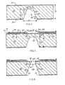
- the process for cutting the common duct 14 through the thickness of the silicon support 20 is as
- a silicon support plate 20 of a thickness in the range between 400 ⁇ m and 700 ⁇ m is passivated on both faces with a layer 22 and 24, respectively, of silicon dioxide with a thickness, for example, of 1.5 ⁇ m, these layers performing the function of thermal and electrical insulation.
- the layers 22 and 24 are covered with two protective layers 26 and 28 of a photosensitive substance.
- photosensitive substances are normally epoxy and/or acrylic resins polymerizable by the effect of light radiation.
- the protective layer 28 is removed by the known photolithographic technique to form an aperture 30 (Fig. 2) of rectangular form extending lengthwise in the direction parallel to the crystallographic orientation ⁇ 110> of the silicon support 20. Consequently, the rows of heating elements 8 and 8′ will be aligned parallel to this direction.
- the aperture 30 leaves free a zone 32 (Fig.2) of the layer 24 of silicon dioxide.
- the zone 32 is thereafter removed chemically with a selective, hydrofluoric acid (HF) based solution to uncover a portion 34 of the support 20 (Fig. 3).
- HF hydrofluoric acid
- the support 20 is constituted by crystalline silicon having a standard crystallographic orientation of ⁇ 100> , the etching action of the anisotropic attack solution develops predominantly in accordance with the orientation of ⁇ 100> and much less in accordance with the associated orientation of ⁇ 111>.
- the orientation ⁇ 100> corresponds to a direction X (Fig. 2) perpendicular to the outer faces of the support 20
- the orientation ⁇ 100> represents a direction Y perpendicular to X
- the orientation ⁇ 111> represents a direction Z perpendicular to Y and forming with the direction X a characteristic angle ⁇ dependent on the form of the crystal lattice of the material of the support 20. Therefore, the groove 35 (Fig. 2)
- a truncated pyramid (Fig. 4) which is obtained after the etching process has in cross-section the form of a truncated pyramid (Fig. 4) having as its greater base the surface 34 (Fig. 3) parallel to the outer faces of the support 20 and as its smaller or truncation base a surface 36 (Fig. 4) parallel to the surface 34, the width L of which depends on the depth H1 reached by the etching and on the width L1 of the zone 34.
- the length of the groove 35 in the direction perpendicular to the drawing depends on the number of nozzles 5 employed in each row.
- the lateral surfaces 38 and 40 have a characteristic inclination ⁇ with respect to the greater base 34 of about 54 o , corresponding to the angle between the crystallographic orientations ⁇ 100> and ⁇ 111> of the silicon support 20.
- etching of the groove 35 (Fig.4) is continued for an attack time T depending on the attack gradient G100 and until the end surface 36 reaches a depth H1 comprised between 60% and 90% of the thickness H of the support 20.
- the depth H1 of the groove 35 to be etched is about 400 ⁇ m.
- the attack time T lasts 8 hours and 55 minutes.
- metal layers are successively deposited under vacuum on the layer 22 of silicon dioxide by known deposition techniques to form the heating elements 8, 8′ and the corresponding electric conductors, for example as described in Italian Patent Application No. 67044 A/89, dated 26.1.89, in the name of the Applicant.
- the silicon dioxide layer 22 is covered with a layer 44 (Fig. 5) between 500 and 2000 A thick of an electrically resistive metal, for example a 50/50 tantalum-aluminium alloy.
- the layer 44 is then etched by a known process of dry etching under vacuum to form two pluralities of independent resistive elements 8 and 8′ for heating the ink.
- the Ta-Al elements 8, 8′ are covered with a layer 46 of aluminium with a thickness comprised between 2000 and 10,000 A.
- the layer 46 is then etched by a process similar to the foregoing to obtain electric conductors 47 for supplying the heating elements 8 and 8′.
- On the aluminium layer 46 there are then deposited two layers 50 and 52 of electrically insulating, but thermally conductive, materials.
- the layer 50 in contact with the aluminium conductors 47 is constituted by silicon nitride, while the overlying layer 52 is constituted by silicon carbide. In total, the two layers 50 and 52 have a thickness compsised between 2000 and 20,000 A.
- a layer 56 of tantalum of a thickness between 1000 A and 10,000 A is thereafter deposited by known techniques on the layer 52.
- the layer 56 is then etched under vacuum to obtain separate and parallel strips superposed on the conductors 47.
- the layer 56 has a dual function of protection of the ink of the subjacent resistive and insulating layers and of electrical connection between the conductors 47 and connecting terminals (not shown) towards the outside.
- the layers 44, 46, 50, 52 and 56 are interrupted in an intermediate zone 60 (Fig. 5) between the two rows of the heating elements 8 and 8′, leaving free a part 62 of the layer 22. More particularly, the tantalum layer 56 also covers the edges 58 of the subjacent layers to protect them from possible infiltrations of acids employed in the etching treatments and from the ink during the operation of the head.
- a jet of sand formed predominantly of alumina particles of an average size of about 20 ⁇ m is directed against the end surface 36 in a direction perpendicular to the surface itself.
- the sandblasting operation is interrupted when an opening 63 (Fig. 6) defined by two plane and parallel walls 64 and 66 has been obtained in the surface 62.
- the walls 64 and 66 are connected at one end to the lateral surfaces 38 and 40, respectively, of the groove 35 and intersect at the other end (at the top in Fig.6) the surface 62.
- the walls 64 and 66 and the surface 62 therefore define a parallelepipedal chamber 69 having the truncation base 36 in common with the pyramidal chamber.
- a layer 74 of photosensitive material for example Vacrel (Registered Trade Mark), in which the chambers 4 and the feed passages 16 are obtained by a photolithographic process.
- a sheet 76 of gold-plated nickel bearing the nozzles 5 and 5′ is hot-soldered to the layer 74.
- thermal ink jet head may undergo variations of modifications and that the thermal head so constructed may be modified in form and dimensions without, however, departing from the scope of the invention.
- the sandblasting process previously described may be substituted alternatively by a process of cutting by means of a laser beam of the "excimer” (excited dimer) type.
- This type of laser is particularly suitable for machining solid materials, such as, for example, silicon and silicon dioxide, inasmuch as the excimer laser operates in a cold state without overheating the parts machined and without leaving traces of melting on the surfaces struck by the laser beam.
- the excimer laser beam generates a very small portion of heat, inasmuch as the energy of the laser beam acts on the molecular bonds of the struck material, overcoming the forces of cohesion.
- the removal of material therefore takes place by ablation of particles, rather than through thermal phenomena such as melting, vaporization or sublimation.
- This mechanism of ablation of particles confers on the machined parts a degree of precision much higher than that obtainable with other conventional types of laser beams, such as a CO2 or YAG laser beam.
- a disc 80 (Fig.7) of silicon of circular form with a diameter of about 100 mm and about 0.5 mm thick is normally used as the supporting base 20.
- a cutaway portion 81 at the edge of the disc 80 commonly indicates the crystallographic orientation ⁇ 100> of the disc 80.
- numerous identical configurations 82 of plates which, when construction has taken place, are separated by means of crossed cuts in the support disc along intermediate lines 83.
- Fig. 8 shows on an enlarged scale a part 84 of the disc 80 comprising a slot 63 seen from the direction of the surface 62 of Fig. 6.
- a panel 85 in chain-dotted lines represents the area occupied on the surface of the disc 80 by the layers 50, 52, 56 (Fig. 5) of each individual plate.
- the process hereinbefore described for etching slots for feeding the ink in each individual plate finds valid application, enabling a plurality of slots of the type of the groove 35 (Fig. 4) to be obtained simultaneously with a single etching operation, with a considerable reduction in the working times and costs.
Landscapes
- Engineering & Computer Science (AREA)
- Manufacturing & Machinery (AREA)
- Particle Formation And Scattering Control In Inkjet Printers (AREA)
Applications Claiming Priority (2)
| Application Number | Priority Date | Filing Date | Title |
|---|---|---|---|
| IT6745889 | 1989-06-08 | ||
| IT8967458A IT1234800B (it) | 1989-06-08 | 1989-06-08 | Procedimento di fabbricazione di testine termiche di stampa a getto d'inchiostro e testine cosi' ottenute |
Publications (2)
| Publication Number | Publication Date |
|---|---|
| EP0401996A2 true EP0401996A2 (de) | 1990-12-12 |
| EP0401996A3 EP0401996A3 (de) | 1991-12-04 |
Family
ID=11302549
Family Applications (1)
| Application Number | Title | Priority Date | Filing Date |
|---|---|---|---|
| EP19900305432 Withdrawn EP0401996A3 (de) | 1989-06-08 | 1990-05-18 | Herstellungsverfahren von thermischen Tintenstrahldruckköpfen sowie auf diese Weise erzeugte Köpfe |
Country Status (2)
| Country | Link |
|---|---|
| EP (1) | EP0401996A3 (de) |
| IT (1) | IT1234800B (de) |
Cited By (13)
| Publication number | Priority date | Publication date | Assignee | Title |
|---|---|---|---|---|
| EP0609012A3 (de) * | 1993-01-25 | 1994-09-14 | Hewlett-Packard Company | Verfahren zum Herstellen eines thermischen Farbstrahldruckkopfs |
| EP0609011A3 (de) * | 1993-01-25 | 1994-09-14 | Hewlett-Packard Company | Verfahren zum Herstellen eines thermischen Farbstrahldruckkopfs |
| EP0764533A3 (de) * | 1995-09-22 | 1997-08-13 | Lexmark Int Inc | Herstellung von Tintenzufuhrkanälen in einem Siliziumsubstrat eines Thermotintenstrahldruckers |
| EP0955166A1 (de) * | 1998-04-29 | 1999-11-10 | Hewlett-Packard Company | Dünnschicht-Tintenstrahldruckkopf |
| WO2000000354A1 (en) * | 1998-06-29 | 2000-01-06 | Olivetti Lexikon S.P.A. | Ink jet printhead |
| WO2001054863A3 (en) * | 2000-01-26 | 2002-04-04 | Hewlett Packard Co | Ink feed slot formation in ink-jet printheads |
| EP1213147A1 (de) * | 2000-12-05 | 2002-06-12 | Hewlett-Packard Company | Geschlitztes Substrat und dazugehöriges Herstellungsverfahren |
| EP1226947A1 (de) * | 2001-01-30 | 2002-07-31 | Hewlett-Packard Company | Dünnfilmbeschichtung eines geschlitzen Substrates und Verfahren zur Herstellung von geschlitzten Substraten |
| WO2002085630A1 (en) * | 2001-04-20 | 2002-10-31 | Hewlett-Packard Company | Thermal ink jet defect tolerant resistor design |
| EP1338420A1 (de) * | 2002-02-20 | 2003-08-27 | Brother Kogyo Kabushiki Kaisha | Tintenstrahlkopf und Tintenstrahldrucker |
| US7267431B2 (en) | 2004-06-30 | 2007-09-11 | Lexmark International, Inc. | Multi-fluid ejection device |
| DE19917595B4 (de) * | 1998-05-29 | 2008-08-07 | Industrial Technology Research Institute, Chutung | Verfahren zum Herstellen eines Tintendruckkopf-Chips sowie dessen Tintendurchlaßkanal-Struktur |
| US7429335B2 (en) | 2004-04-29 | 2008-09-30 | Shen Buswell | Substrate passage formation |
Families Citing this family (1)
| Publication number | Priority date | Publication date | Assignee | Title |
|---|---|---|---|---|
| ITTO20020876A1 (it) | 2002-10-10 | 2004-04-11 | Olivetti I Jet Spa | Dispositivo di stampa a getto di inchiostro in parallelo |
Family Cites Families (4)
| Publication number | Priority date | Publication date | Assignee | Title |
|---|---|---|---|---|
| US4601777A (en) * | 1985-04-03 | 1986-07-22 | Xerox Corporation | Thermal ink jet printhead and process therefor |
| DE3682569D1 (de) * | 1985-12-06 | 1992-01-02 | Hewlett Packard Co | Aufbau eines waermetintenduesen-druckkopfes. |
| US4789425A (en) * | 1987-08-06 | 1988-12-06 | Xerox Corporation | Thermal ink jet printhead fabricating process |
| US4835553A (en) * | 1988-08-25 | 1989-05-30 | Xerox Corporation | Thermal ink jet printhead with increased drop generation rate |
-
1989
- 1989-06-08 IT IT8967458A patent/IT1234800B/it active
-
1990
- 1990-05-18 EP EP19900305432 patent/EP0401996A3/de not_active Withdrawn
Cited By (23)
| Publication number | Priority date | Publication date | Assignee | Title |
|---|---|---|---|---|
| EP0609012A3 (de) * | 1993-01-25 | 1994-09-14 | Hewlett-Packard Company | Verfahren zum Herstellen eines thermischen Farbstrahldruckkopfs |
| EP0609011A3 (de) * | 1993-01-25 | 1994-09-14 | Hewlett-Packard Company | Verfahren zum Herstellen eines thermischen Farbstrahldruckkopfs |
| US5441593A (en) * | 1993-01-25 | 1995-08-15 | Hewlett-Packard Corporation | Fabrication of ink fill slots in thermal ink-jet printheads utilizing chemical micromachining |
| US5608436A (en) * | 1993-01-25 | 1997-03-04 | Hewlett-Packard Company | Inkjet printer printhead having equalized shelf length |
| EP0764533A3 (de) * | 1995-09-22 | 1997-08-13 | Lexmark Int Inc | Herstellung von Tintenzufuhrkanälen in einem Siliziumsubstrat eines Thermotintenstrahldruckers |
| EP0955166A1 (de) * | 1998-04-29 | 1999-11-10 | Hewlett-Packard Company | Dünnschicht-Tintenstrahldruckkopf |
| US6126277A (en) * | 1998-04-29 | 2000-10-03 | Hewlett-Packard Company | Non-kogating, low turn on energy thin film structure for very low drop volume thermal ink jet pens |
| DE19917595B4 (de) * | 1998-05-29 | 2008-08-07 | Industrial Technology Research Institute, Chutung | Verfahren zum Herstellen eines Tintendruckkopf-Chips sowie dessen Tintendurchlaßkanal-Struktur |
| US6412921B1 (en) | 1998-06-29 | 2002-07-02 | Olivetti Tecnost S.P.A. | Ink jet printhead |
| WO2000000354A1 (en) * | 1998-06-29 | 2000-01-06 | Olivetti Lexikon S.P.A. | Ink jet printhead |
| WO2001054863A3 (en) * | 2000-01-26 | 2002-04-04 | Hewlett Packard Co | Ink feed slot formation in ink-jet printheads |
| US6968617B2 (en) | 2000-12-05 | 2005-11-29 | Hewlett-Packard Development Company, L.P. | Methods of fabricating fluid ejection devices |
| US6675476B2 (en) | 2000-12-05 | 2004-01-13 | Hewlett-Packard Development Company, L.P. | Slotted substrates and techniques for forming same |
| SG115428A1 (en) * | 2000-12-05 | 2005-10-28 | Hewlett Packard Co | Slotted substrates and techniques for forming same |
| EP1213147A1 (de) * | 2000-12-05 | 2002-06-12 | Hewlett-Packard Company | Geschlitztes Substrat und dazugehöriges Herstellungsverfahren |
| EP1226947A1 (de) * | 2001-01-30 | 2002-07-31 | Hewlett-Packard Company | Dünnfilmbeschichtung eines geschlitzen Substrates und Verfahren zur Herstellung von geschlitzten Substraten |
| WO2002085630A1 (en) * | 2001-04-20 | 2002-10-31 | Hewlett-Packard Company | Thermal ink jet defect tolerant resistor design |
| US6527378B2 (en) | 2001-04-20 | 2003-03-04 | Hewlett-Packard Company | Thermal ink jet defect tolerant resistor design |
| US6832434B2 (en) | 2001-04-20 | 2004-12-21 | Hewlett-Packard Development Company, L.P. | Methods of forming thermal ink jet resistor structures for use in nucleating ink |
| EP1338420A1 (de) * | 2002-02-20 | 2003-08-27 | Brother Kogyo Kabushiki Kaisha | Tintenstrahlkopf und Tintenstrahldrucker |
| US6979077B2 (en) | 2002-02-20 | 2005-12-27 | Brother Kogyo Kabushiki Kaisha | Ink-jet head and ink-jet printer having ink-jet head |
| US7429335B2 (en) | 2004-04-29 | 2008-09-30 | Shen Buswell | Substrate passage formation |
| US7267431B2 (en) | 2004-06-30 | 2007-09-11 | Lexmark International, Inc. | Multi-fluid ejection device |
Also Published As
| Publication number | Publication date |
|---|---|
| IT1234800B (it) | 1992-05-27 |
| EP0401996A3 (de) | 1991-12-04 |
| IT8967458A0 (it) | 1989-06-08 |
Similar Documents
| Publication | Publication Date | Title |
|---|---|---|
| EP0764533B1 (de) | Herstellung von Tintenzufuhrkanälen in einem Siliziumsubstrat eines Thermotintenstrahldruckers | |
| EP0376514B1 (de) | Herstellungsverfahren für Gross-Matrix-Halbleiterbauelemente | |
| US5000811A (en) | Precision buttable subunits via dicing | |
| US4951063A (en) | Heating elements for thermal ink jet devices | |
| EP0244214B1 (de) | Thermischer Tintenstrahldruckkopf | |
| EP0321075B1 (de) | Integrierter Tintenspritzdruckkopf und Verfahren zu dessen Herstellung | |
| EP0895866B1 (de) | Herstellen eines Tintenkanals für einen Tintenstrahldruckkopf | |
| EP0370776B1 (de) | Herstellungsverfahren eines Farbstrahldruckkopfes | |
| EP0509669B1 (de) | Düsenplatte für thermische Tintenstrahldruckerköpfe sowie Herstellungsverfahren | |
| EP0430593B1 (de) | Verfahren zum Schneiden eines Substrates aus Silizium mittels einer preferentiellen Ätzung | |
| US4899181A (en) | Large monolithic thermal ink jet printhead | |
| US5057853A (en) | Thermal ink jet printhead with stepped nozzle face and method of fabrication therefor | |
| JPH08467B2 (ja) | インク・ジェット印字ヘッド製造方法 | |
| EP0609012A3 (de) | Verfahren zum Herstellen eines thermischen Farbstrahldruckkopfs | |
| TW200406313A (en) | Slotted substrate and method of making | |
| JPH02229050A (ja) | インクジェットプリントヘッドを製造する方法 | |
| CN102009527A (zh) | 制造液体排出头基材的方法 | |
| EP1213147B1 (de) | Geschlitztes Substrat und dazugehöriges Herstellungsverfahren | |
| EP0401996A3 (de) | Herstellungsverfahren von thermischen Tintenstrahldruckköpfen sowie auf diese Weise erzeugte Köpfe | |
| US20040075717A1 (en) | Wafer processing apparatus and method | |
| US4194211A (en) | Charge electrode array for multi-nozzle ink jet array | |
| EP0110534B1 (de) | Monolithische Tintenstrahldüsenöffnungsplatten/Widerstandskombination | |
| EP1439959B1 (de) | Verfahren zum herstellen eines zuführkanals für einen tintenstrahldruckkopf | |
| JP2865524B2 (ja) | サーマルインクジェットヘッド | |
| US6668453B1 (en) | Method for manufacturing ink jet recording head |
Legal Events
| Date | Code | Title | Description |
|---|---|---|---|
| PUAI | Public reference made under article 153(3) epc to a published international application that has entered the european phase |
Free format text: ORIGINAL CODE: 0009012 |
|
| AK | Designated contracting states |
Kind code of ref document: A2 Designated state(s): DE FR GB |
|
| PUAL | Search report despatched |
Free format text: ORIGINAL CODE: 0009013 |
|
| AK | Designated contracting states |
Kind code of ref document: A3 Designated state(s): DE FR GB |
|
| RHK1 | Main classification (correction) |
Ipc: B41J 2/16 |
|
| 17P | Request for examination filed |
Effective date: 19920526 |
|
| 17Q | First examination report despatched |
Effective date: 19931207 |
|
| STAA | Information on the status of an ep patent application or granted ep patent |
Free format text: STATUS: THE APPLICATION IS DEEMED TO BE WITHDRAWN |
|
| 18D | Application deemed to be withdrawn |
Effective date: 19940618 |