EP1439959B1 - Verfahren zum herstellen eines zuführkanals für einen tintenstrahldruckkopf - Google Patents
Verfahren zum herstellen eines zuführkanals für einen tintenstrahldruckkopf Download PDFInfo
- Publication number
- EP1439959B1 EP1439959B1 EP02788533A EP02788533A EP1439959B1 EP 1439959 B1 EP1439959 B1 EP 1439959B1 EP 02788533 A EP02788533 A EP 02788533A EP 02788533 A EP02788533 A EP 02788533A EP 1439959 B1 EP1439959 B1 EP 1439959B1
- Authority
- EP
- European Patent Office
- Prior art keywords
- front surface
- substrate
- stage
- process according
- diaphragm
- Prior art date
- Legal status (The legal status is an assumption and is not a legal conclusion. Google has not performed a legal analysis and makes no representation as to the accuracy of the status listed.)
- Expired - Lifetime
Links
Images

Classifications
-
- B—PERFORMING OPERATIONS; TRANSPORTING
- B41—PRINTING; LINING MACHINES; TYPEWRITERS; STAMPS
- B41J—TYPEWRITERS; SELECTIVE PRINTING MECHANISMS, i.e. MECHANISMS PRINTING OTHERWISE THAN FROM A FORME; CORRECTION OF TYPOGRAPHICAL ERRORS
- B41J2/00—Typewriters or selective printing mechanisms characterised by the printing or marking process for which they are designed
- B41J2/005—Typewriters or selective printing mechanisms characterised by the printing or marking process for which they are designed characterised by bringing liquid or particles selectively into contact with a printing material
- B41J2/01—Ink jet
- B41J2/135—Nozzles
- B41J2/16—Production of nozzles
- B41J2/1621—Manufacturing processes
- B41J2/1626—Manufacturing processes etching
- B41J2/1628—Manufacturing processes etching dry etching
-
- B—PERFORMING OPERATIONS; TRANSPORTING
- B41—PRINTING; LINING MACHINES; TYPEWRITERS; STAMPS
- B41J—TYPEWRITERS; SELECTIVE PRINTING MECHANISMS, i.e. MECHANISMS PRINTING OTHERWISE THAN FROM A FORME; CORRECTION OF TYPOGRAPHICAL ERRORS
- B41J2/00—Typewriters or selective printing mechanisms characterised by the printing or marking process for which they are designed
- B41J2/005—Typewriters or selective printing mechanisms characterised by the printing or marking process for which they are designed characterised by bringing liquid or particles selectively into contact with a printing material
- B41J2/01—Ink jet
- B41J2/135—Nozzles
- B41J2/16—Production of nozzles
- B41J2/1601—Production of bubble jet print heads
- B41J2/1603—Production of bubble jet print heads of the front shooter type
-
- B—PERFORMING OPERATIONS; TRANSPORTING
- B41—PRINTING; LINING MACHINES; TYPEWRITERS; STAMPS
- B41J—TYPEWRITERS; SELECTIVE PRINTING MECHANISMS, i.e. MECHANISMS PRINTING OTHERWISE THAN FROM A FORME; CORRECTION OF TYPOGRAPHICAL ERRORS
- B41J2/00—Typewriters or selective printing mechanisms characterised by the printing or marking process for which they are designed
- B41J2/005—Typewriters or selective printing mechanisms characterised by the printing or marking process for which they are designed characterised by bringing liquid or particles selectively into contact with a printing material
- B41J2/01—Ink jet
- B41J2/135—Nozzles
- B41J2/16—Production of nozzles
- B41J2/1621—Manufacturing processes
- B41J2/1631—Manufacturing processes photolithography
-
- B—PERFORMING OPERATIONS; TRANSPORTING
- B41—PRINTING; LINING MACHINES; TYPEWRITERS; STAMPS
- B41J—TYPEWRITERS; SELECTIVE PRINTING MECHANISMS, i.e. MECHANISMS PRINTING OTHERWISE THAN FROM A FORME; CORRECTION OF TYPOGRAPHICAL ERRORS
- B41J2/00—Typewriters or selective printing mechanisms characterised by the printing or marking process for which they are designed
- B41J2/005—Typewriters or selective printing mechanisms characterised by the printing or marking process for which they are designed characterised by bringing liquid or particles selectively into contact with a printing material
- B41J2/01—Ink jet
- B41J2/135—Nozzles
- B41J2/16—Production of nozzles
- B41J2/1621—Manufacturing processes
- B41J2/1632—Manufacturing processes machining
Definitions
- This invention relates to an improved process for construction of a feeding duct for an ink jet printhead, particularly for a "top-shooter” type ink jet printhead, i.e. one in which the droplets of ink are ejected perpendicularly to the substrate containing the expulsion chambers and the heating elements.
- a printhead of the above-mentioned type is made using as the substrate a portion of a thin disk of crystalline silicon approx.
- the heating elements or resistors, made of portions of an electrically conducting layer and the relative connections with the outside;
- the resistors are arranged inside cells made in the thickness of a layer of photosensitive material, for instance VACREL TM, and obtained together with the lateral ink feeding channels in a photolithographic process;
- the cells are filled with a volume of ink fed through a narrow, oblong feeding duct, shaped as a slot, which traverses the silicon substrate and communicates with the lateral channels of the cells.
- the slots are made with a wet etching applied to the end opposite the cells, and completed with a laser etching, or with sand blasting.
- the known techniques for etching of the slots have the drawback that the edge of the slot facing the cells has geometrical irregularities caused either by the action of the grains of abrasive used for sand blasting, or by cracks and fissures caused by an incipient melting of the material if a laser beam is used for the etching; these irregularities disturb the flow of ink at the entrance to the cells and are particularly damaging in the case of very narrow slots, i.e. of width less than 250 ⁇ m approx., and in multiple heads with slots side by side in the same portion of the silicon substrate.
- the main object of this invention is therefore that of defining an improved process for the manufacture of a feeding duct for an ink jet printhead exempt of the drawbacks mentioned above and in particular having a slot-like aperture of a very low width local to the expulsion cells, to permit multiple heads, and/or heads with a large number of nozzles, to be produced on the same silicon substrate, capable of ejecting very small droplets ( ⁇ 5 pl), particularly suitable for printing images with photographic resolution.
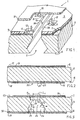
- the head 1 is made of a support element or dice 3 of crystalline silicon, cut from a larger disc or wafer with crystallographic orientation ⁇ 100> (fig. 4), and of thickness between 500 and 600 ⁇ m, delimited by two opposite surfaces 5 and 6 (fig. 1), flat and parallel, respectively called front surface 5 and rear surface 6 for clarity of the description.
- a plurality of cells 8 for expulsion of the ink are made in the thickness of a layer of photosensitive type resin 9, known in the sector art, and communicate hydraulically through channels 10 with the feeding duct 2, constructed according to the process the subject of this invention.
- each cell 8 On the bottom of each cell 8 are the heating elements 11, made in a known way, from a layer of electrically resistive material, placed between isolating layers made of silicon nitrides and carbides; the heating elements 11 are in turn electrically connected to electric conductors 12 made in a layer of conducting material, such as aluminium, tantalum, etc. which are connected to external electronic circuits for supplying the electrical pulses for expulsion of the droplets of ink.
- a lamina 14 is stuck, which may be of a metal, such as gold, or nickel, or an alloy thereof, or of a resin, such as KaptonTM, which bears the nozzles 15 for ejection of the ink droplets, arranged in correspondence with each cell 8.
- the substrate 3 (fig. 2) is previously passivated on both its opposite surfaces 5 and 6 via the depositing of a dielectric and thermally isolating layer, 17 and 18 respectively, of SiO 2, having a thickness of approx. 1.5 ⁇ m.
- the layers 17, 18 constitute a flat and homogeneous base for anchoring the further layers deposited during construction of the head 1.
- Each of the layers 17 and 18 is coated with a protective layer 19 of a photosensitive substance.
- the photosensitive substance normally consists of epoxy and/or acrylic resins, polimerisable through the effect of light radiations.
- the aperture 20 leaves uncovered a zone 21 of the underlying layer 18 of SiO 2 , suitable for being corroded subsequently and chemically removed with a selective etching solution based on hydrofluoric acid (HF), to free a corresponding area 22 of the silicon substrate 3 (fig. 2).
- a selective etching solution based on hydrofluoric acid (HF) to free a corresponding area 22 of the silicon substrate 3 (fig. 2).
- the work for producing the feeding duct 2, according to this invention starts on the rear surface 6, with a dry etching operation, for instance sand-blasting, of the area 22, performed for a depth P 1 of approx. 30% of the thickness of the substrate 3 (fig. 3); with this operation and using a substrate 3 of silicon of about 600 ⁇ m thick, a first cavity 24 of depth P 1 of about 180 ⁇ m is obtained, with side walls 25 (dashed line) perpendicular to the surface 6 of the substrate 3.
- a dry etching operation for instance sand-blasting
- the work continues with an anisotropic electrolytic corrosion operation, in a chemical etching bath, using one of the known anisotropic solutions based on ethylenediamine and pyrocatechol, or based on potassium hydroxide, or again on hydrazine.
- Each of the solutions used has a maximum etching gradient "G 100 ", which develops according to the direction of the crystallographic axis ⁇ 100> of the substrate 3 and varying between 0.75 and 1.8 ⁇ m/min, at a temperature of roughly 90°C, whereas the ratio G 100 /G 111 , where G 111 is the gradient of anisotropic etching according to the crystallographic axis direction ⁇ 111>, may range between 35 : 1 and 400 : 1.
- the chemical etching in this stage of the process proceeds preferably in the characteristic direction ⁇ 100> and much less in the direction ⁇ 111>, inclined by an angle ⁇ of approximately 54° with respect to the surfaces 5 and 6 of the substrate 3 (fig. 4); the chemical corrosion in this stage therefore produces a further cavity 26, (fig. 3) communicating with the cavity 24 and bound by lateral walls 27, inclined by the angle ⁇ with respect to the surface 6 of the substrate 3 and by a rear wall 28, opposite the cavity 24.
- the depth P 2 of the cavity 26, reached in the direction perpendicular to the surface 6, depends on the gradient of etching G 100 of the etching solution employed and by the time taken.
- the chemical etching action is continued until such time as the depth P 2 of the cavity 26 reaches a prefixed value of approximately 50% of the thickness of the substrate 3, while the rear wall 28 of the excavation attains a width L1 of approximately 150 ⁇ m, so as to leave a diaphragm 30 between the rear wall 28 and the front surface 5 of thickness P 3 of approximately 100 ⁇ m +/- 20 ⁇ m, equal to roughly 15% - 20% of the thickness of the substrate 3.
- the construction of the feeding duct 2 is interrupted in order to proceed to deposition on the front surface 5 (fig. 4) of a plurality of layers 7 necessary to create the heating elements 11, the relative electric conductors 12 (fig. 1), coated in turn with protective layers of silicon nitride and carbide 13, and a layer 16 of tantalum protecting the underlying zone containing the heating elements.
- a layer 34 of positive photoresist about 5 ⁇ m thick is deposited, which protects the other layers 7 during subsequent work and completely fills up a recess 33 created when, in the zone 2a in which the feeding duct 2 will be opened, all the existing layers 17, 19, 13, 16 have been removed with a dry etching process, known in the sector art, leaving free an area 32 of bare silicon of the substrate 3.
- the layer 34 of photoresist is exposed through a thin mask 35, of a particular design, according to this invention, and developed in order to bound the outlet area 2a (fig. 4) of the feeding duct 2, in correspondence with the front surface 5.
- the mask 35 used in this stage of the manufacturing process contains an aperture 36 consisting of a groove 37 of width Ls, in the shape of a closed, narrow ring elongated in a direction parallel to the crystallographic direction ⁇ 110> of the silicon substrate 3.
- the width Ls of the groove 37 is preferably established as 10 - 50 ⁇ m, whereas the distance La between the external, opposite long sides 38 of the aperture 36 is between 100 and 130 ⁇ m, and in any case not greater than the width L1 defined above.
- the external long sides 38 of the groove 37 and the distance La between them define respectively the profile and the width of the final outlet aperture 2a of the feeding duct 2, in correspondence with the front surface 5; the length of the long sides 38 in the direction ⁇ 110> depends mainly on the number of nozzles foreseen.
- the next step of the process consists in removing the material in the area of the groove 37 in the direction of the rear wall 28, to form a channel 40 (fig. 5) in the silicon substrate 3, in the thickness P 3 of the diaphragm 30, over a depth P 4 of 20 - 50 ⁇ m.
- Etching of the channel 40 is performed with a dry etching technique, known to those acquainted with the sector art, to form with the greatest precision allowed the edges 39 of the channel 37, namely the corner between the channel itself and the front surface 5, and to obtain the distance La between the edges 39 reduced to values of less than 150 ⁇ m and preferably to approx. 100 ⁇ m.
- a film 9 (fig. 1, 6) of a photosensitive material, consisting of a negative photopolymer, for example VacrelTM , is laminated, and on this are produced in a photolithographic process the ejection cells 8 and the associated feeding channels 10.
- a protective layer 44 of EmulsitoneTM (fig. 6) which penetrates the groove 40 and prevents shavings from being deposited in the area already worked, in the cells 8 for instance, and avoids further damage in successive work steps.
- the diaphragm 30 is taken away in a cutting operation, preferably employing a beam of copper vapour laser rays; this choice is dictated by the fact that the copper vapour laser allows cutting with extremely high precision of the diaphragm 30, with a low heating of the material around the cut.
- the laser beam is applied from the rear surface 6 side, against the wall 28 of the recess 26, and is interrupted when the cut reaches the bottom of the channel 40; by using a laser cut, the walls of the channel thus formed remain perfectly delimited and above all, the layers comprising the head 1 in close proximity of the cutting zone are not damaged, thanks to the limited heating generated by the laser.
- progressive sand-blasting may be used to take away the diaphragm 30, where applied from the rear part of the substrate 3, against the wall 28, taking care to successively erode thin layers of material, for example by bringing the sand-blasting nozzle progressively closer, until the cutting reaches the bottom of the channel 40, and results in the detachment of the portion of silicon 45 located inside.
- the feeding duct 2 is made in three successive stages, of which the first stage and the third stage are performed at the rear of the substrate 3, while the second stage is performed at the front.
- the edge of the feeding duct at the outlet 2a in correspondence with the front surface 5 is produced in the second stage, obtaining maximal precision of dimensions and surface finish, ensured by employing a dry etching in an area with perfectly delineated contours, which can only be obtained by using a mask 35.
- a sheet of KaptonTM 14 (fig. 1), bearing one or more rows of nozzles 15, is heat glued on top of the layer 9 containing the cells 8 and the associated feeding channels 10, where each nozzle is placed with the maximum precision in correspondence with the corresponding ejection cell.
Landscapes
- Engineering & Computer Science (AREA)
- Manufacturing & Machinery (AREA)
- Particle Formation And Scattering Control In Inkjet Printers (AREA)
- Ink Jet (AREA)
Claims (14)
- Verfahren zur Herstellung eines Zuführkanals für einen Tintenstrahldruckkopf desjenigen Typs aufweisend:dadurch gekennzeichnet ist, dassein Substrat (3) aus Silizium einer bestimmten Dicke, wobei das Substrat durch eine vordere Oberfläche (5) und eine hintere Oberfläche (6) begrenzt ist, die einander gegenüberliegend, flach und parallel zueinander sind und die beide durch eine Passivierschicht aus dielektrischem Material (17, 18) geschützt sind,mehrere Tintenausstoßzellen (8), denen durch einen Kanal (2), der durch das Siliziumsubstrat (3) verläuft, Tinte zugeführt wird,mehrere Heizelemente (11) entsprechend den mehreren Ausstoßzellen (8), wobei die Heizelemente (11) im Innern der Zellen (8) angeordnet sind und eine bestimmte Tintenmenge ausstoßen können, undmehrere elektrische Leiter (12), die mit den Heizelementen (11) verbunden sind, wobeidie mehreren Tintenausstoßzellen (8), die mehreren Heizelemente (11) und die mehreren elektrischen Leiter (12) in verschiedenen übereinander liegenden Schichten gebildet sind, die auf die vordere Oberfläche (5) aufgebracht sind, und wobei das Verfahren zur Herstellung eines Zuführkanals (2)
es drei aufeinanderfolgende Stufen zur Abtragung des Siliziumsubstrats (3) umfasst, von denen die erste Stufe an der hinteren Oberfläche (6) des Substrats (3) durchgeführt, die zweite Stufe an der vorderen Oberfläche (5) des Substrats (3) durchgeführt, und die dritte Stufe an der hinteren Oberfläche (6) als Fortsetzung der in der ersten Stufe erfolgten Abtragung durchgeführt wird. - Verfahren nach Anspruch 1,
dadurch gekennzeichnet, dass
die erste Stufe die folgenden Schritte aufweist:a) Festlegen eines ersten Bereichs (22) einer vorbestimmten Form an der hinteren Oberfläche (6) gegenüberliegend der vorderen Oberfläche (5);b1) Ätzen des Substrats (3) durch einen Trocknungsvorgang in dem Bereich (22), um eine erste Ausnehmung (24) mit Seitenwänden (25) zu bilden, die senkrecht zur hinteren Oberfläche (6) angeordnet sind und die sich durch die Dicke in Richtung der vorderen Oberfläche (5) in einer vorbestimmten Tiefe (P1) erstrecken;b2) Fortführen des Ätzens der Ausnehmung (24) durch eine anisotrope elektrolytische Korrosion unter Verwendung einer anisotropen chemischen Verbindung zum Ätzen für eine vorgegebene Ätzdauer, um eine weitere Ausnehmung (26) zu bilden, die mit der ersten Ausnehmung (24) in Verbindung steht, und die sich durch die Dicke in Richtung der vorderen Oberfläche (5) über eine Tiefe (P2) erstreckt und eine hintere Wand (28) aufweist, die senkrecht zu dieser Richtung ist und eine Membran (30) einer bestimmten Dicke (P3) bezüglich der vorderen Oberfläche (5) bildet; die zweite Stufe die folgenden Schritte umfasst:c) Festlegen eines zweiten Bereichs (36) an der vorderen Oberfläche (5), der ringförmig, länglich und parallel zu einer charakteristischen kristallographischen Richtung (<100>) des Substrats (3) ist;d) Ätzen des Substrats (3) mit einem Trockenverfahren in dem zweiten Bereich (36) für eine vorbestimmte Tiefe (P4) in die Membran (30) in Richtung der hinteren Wand (28), um eine ringförmige Nut (40) zu bilden, die die Randkontur (39) des endgültigen Zuführkanals (2a) in Übereinstimmung mit der vorderen Oberfläche (5) festlegt, und wobei
die dritte Stufe die folgenden Schritte umfasst:e) Schrittweise Abtragen der Membran (30) von der hinteren Oberfläche (6) beginnend von der hinteren Wand (28) in Richtung der vorderen Oberfläche (5), bis die ringförmige Nut (40) erreicht ist, um den Zuführkanal (2) zwischen der vorderen Oberfläche (5) und der hinteren Oberfläche (6) zu öffnen. - Verfahren nach Anspruch 1,
dadurch gekennzeichnet, dass
die Tiefe (P1) des Hohlraums (26) in etwa 30% der Dicke des Substrats (3) beträgt. - Verfahren nach Anspruch 1 oder 2,
dadurch gekennzeichnet, dass
die Tiefe (P2) in etwa 50% der Dicke des Substrats (3) beträgt. - Verfahren nach einem der Ansprüche 1 bis 4,
dadurch gekennzeichnet, dass
der Schritt b2) die Verwendung eines chemischen Ätzbades vorsieht, das sich aus einer anisotropen wässrigen Lösung aus Ethylenediamin und Pyrocatechol, aus Potassium-Hydroxid, oder aus Hydrazin zusammensetzt. - Verfahren nach Anspruch 5,
dadurch gekennzeichnet, dass
der Schritt b2) darüber hinaus das Unterbrechen der chemischen Korrosion des Hohlraums (26) vorsieht, wenn die Dicke (P3) der Membran (30) in etwa 15% - 20% der Dicke des Substrats (3) erreicht hat, und die Breite (L1) der hinteren Wand (28) 100 - 130 µm misst. - Verfahren nach einem der vorhergehenden Ansprüche,
dadurch gekennzeichnet, dass
der Schritt e) die Verwendung eines Kupferdampflasers vorsieht. - Verfahren nach Anspruch 1,
dadurch gekennzeichnet, dass
der Schritt e) das schrittweise Aufbringen eines Sandstrahls umfasst, um nach und nach dünne Schichten der Membran (30) zu entfernen. - Verfahren nach einem der vorhergehenden Ansprüche,
dadurch gekennzeichnet, dass
der Schritt c) die Verwendung einer Schicht (34) aus einem positiven Photoresist einer Dicke von in etwa 5 µm umfasst, die unter Verwendung einer Maske mit einer Öffnung (36) in Form einer schmalen ringförmigen Nut (37), die in Richtung parallel zur kristallografischen Richtung <110> des Substrats verlängert ist, belichtet und entwickelt wird, um den Auslassbereich (2a) des Zuführkanals (2) in Übereinstimmung mit der vorderen Oberfläche (5) zu begrenzen. - Verfahren nach einem der vorhergehenden Ansprüche,
dadurch gekennzeichnet, dass
die Tiefe (P4) des ringförmigen Kanals (40) mit in etwa 20 - 50 µm vorgegeben ist. - Verfahren nach einem der vorhergehenden Ansprüche,
dadurch gekennzeichnet, dass
vor der zweiten Stufe das Aufbringen auf die vordere Oberfläche (5) von mehreren Schichten (7) erfolgt, die zur Bildung der Heizelemente (11) erforderlich sind, wobei die elektrischen Leiter (12) wiederum mit Schutzschichten aus Siliziumnitrit und -karbit (13) und einer Schicht (16) aus Tantalum überzogen sind, welche den darunter befindlichen Bereich schützten, der die Heizelemente (11) enthält. - Verfahren nach Anspruch 11,
dadurch gekennzeichnet, dass
vor der dritten Stufe das Bilden der Zellen (8) in einer Schicht (9) aus photoempfindlichem Material erfolgt, das auf die mehreren Schichten (7) aufgebracht ist. - Verfahren nach Anspruch 12,
dadurch gekennzeichnet, dass
nach der dritten Stufe auf die Schicht aus photoempfindlichem Material eine Schicht (14) geklebt wird, die mehrere Düsen (15) trägt, die mit jeweiligen Zellen (8) ausgerichtet sind, um Tintentröpfchen auszustoßen. - Tintenstrahldruckkopf, bei dem Tintentröpfchen durch mehrere Düsen von entsprechenden Ausstoßzellen (8) ausgestoßen werden, die in einer Schicht (8) aus mehreren Schichten (7) gebildet sind, die auf ein Siliziumsubstrat aufgebracht sind, das durch eine vordere Oberfläche (5) und durch eine gegenüberliegende, flache, parallele hintere Oberfläche (6) begrenzt ist, wobei den Zellen (8) durch einen Zuführkanal (2), der sich durch das Substrat (3) erstreckt und einen Auslassbereich (2a) an der vorderen Oberfläche (5) hat, Tinte zugeführt wird,
dadurch gekennzeichnet, dass
der Kanal (2) in drei aufeinanderfolgenden Stufen zur Abtragung des Substrats (3) hergestellt wird, von denendie erste Stufe an der hinteren Oberfläche (6) erfolgt, um einen ersten Hohlraum (24) mit einer vorgegebenen Tiefe (P1) und einen weiteren Hohlraum (26) zu bilden, der in Verbindung steht und eine vorgegebene Tiefe (P2) hat, die sich in Richtung der vorderen Oberfläche (5) erstreckt, und eine hintere Wand (28) hat, die von der vorderen Oberfläche (5) durch eine Membran (30) getrennt ist,die zweite Stufe an der gegenüberliegenden vorderen Oberfläche (5) durchgeführt wird, um einen Kanal (40) in Richtung der Membran (30) mit einer vorgegebenen Tiefe (P4) zu ätzen und die Kontur des Auslassbereichs (2a) festzulegen, unddie dritte Stufe von der hinteren Oberfläche (6) aus als eine Fortführung der in der ersten Stufe erfolgten Abtragung durchgeführt wird, um die Membran (30) zu entfernen und den Kanal (2) zwischen der hinteren (6) und der vorderen (5) Oberfläche zu öffnen.
Applications Claiming Priority (3)
| Application Number | Priority Date | Filing Date | Title |
|---|---|---|---|
| IT2001TO001019A ITTO20011019A1 (it) | 2001-10-25 | 2001-10-25 | Procedimento perfezionato per la costruzione di un condotto di alimentazione per una testina di stampa a getto di inchiostro. |
| ITTO20011019 | 2001-10-25 | ||
| PCT/IT2002/000678 WO2003035401A1 (en) | 2001-10-25 | 2002-10-24 | Improved process for construction of a feeding duct for an ink jet printhead |
Publications (3)
| Publication Number | Publication Date |
|---|---|
| EP1439959A1 EP1439959A1 (de) | 2004-07-28 |
| EP1439959B1 true EP1439959B1 (de) | 2005-05-18 |
| EP1439959B8 EP1439959B8 (de) | 2005-07-13 |
Family
ID=11459276
Family Applications (1)
| Application Number | Title | Priority Date | Filing Date |
|---|---|---|---|
| EP02788533A Expired - Lifetime EP1439959B8 (de) | 2001-10-25 | 2002-10-24 | Verfahren zum herstellen eines zuführkanals für einen tintenstrahldruckkopf |
Country Status (7)
| Country | Link |
|---|---|
| US (1) | US7229157B2 (de) |
| EP (1) | EP1439959B8 (de) |
| AT (1) | ATE295784T1 (de) |
| DE (1) | DE60204237T2 (de) |
| ES (1) | ES2243782T3 (de) |
| IT (1) | ITTO20011019A1 (de) |
| WO (1) | WO2003035401A1 (de) |
Families Citing this family (5)
| Publication number | Priority date | Publication date | Assignee | Title |
|---|---|---|---|---|
| ITTO20020876A1 (it) | 2002-10-10 | 2004-04-11 | Olivetti I Jet Spa | Dispositivo di stampa a getto di inchiostro in parallelo |
| JP2008126504A (ja) * | 2006-11-20 | 2008-06-05 | Canon Inc | インクジェット記録ヘッドの製造方法、およびインクジェット記録ヘッド |
| US9707586B2 (en) | 2012-03-16 | 2017-07-18 | Hewlett-Packard Development Company, L.P. | Printhead with recessed slot ends |
| JP6168909B2 (ja) * | 2013-08-13 | 2017-07-26 | キヤノン株式会社 | 液体吐出ヘッド用基板の製造方法 |
| TWI553793B (zh) * | 2014-07-24 | 2016-10-11 | 光頡科技股份有限公司 | 陶瓷基板、封裝基板、半導體晶片封裝件及其製造方法 |
Family Cites Families (8)
| Publication number | Priority date | Publication date | Assignee | Title |
|---|---|---|---|---|
| US4169008A (en) | 1977-06-13 | 1979-09-25 | International Business Machines Corporation | Process for producing uniform nozzle orifices in silicon wafers |
| US4961821A (en) | 1989-11-22 | 1990-10-09 | Xerox Corporation | Ode through holes and butt edges without edge dicing |
| US5387314A (en) | 1993-01-25 | 1995-02-07 | Hewlett-Packard Company | Fabrication of ink fill slots in thermal ink-jet printheads utilizing chemical micromachining |
| US5658471A (en) | 1995-09-22 | 1997-08-19 | Lexmark International, Inc. | Fabrication of thermal ink-jet feed slots in a silicon substrate |
| DK0841167T3 (da) | 1996-11-11 | 2005-01-24 | Canon Kk | Fremgangsmåde til fremstilling af gennemgående hul og anvendelse af den nævnte fremgangsmåde til fremstilling af et siliciumsubstrat, der har et gennemgående hul, og en anordning, der anvender et sådant substrat, fremgangsmåde til fremstilling..... |
| US6164762A (en) * | 1998-06-19 | 2000-12-26 | Lexmark International, Inc. | Heater chip module and process for making same |
| US6402301B1 (en) * | 2000-10-27 | 2002-06-11 | Lexmark International, Inc | Ink jet printheads and methods therefor |
| US6805432B1 (en) * | 2001-07-31 | 2004-10-19 | Hewlett-Packard Development Company, L.P. | Fluid ejecting device with fluid feed slot |
-
2001
- 2001-10-25 IT IT2001TO001019A patent/ITTO20011019A1/it unknown
-
2002
- 2002-10-24 WO PCT/IT2002/000678 patent/WO2003035401A1/en not_active Ceased
- 2002-10-24 DE DE60204237T patent/DE60204237T2/de not_active Expired - Lifetime
- 2002-10-24 AT AT02788533T patent/ATE295784T1/de not_active IP Right Cessation
- 2002-10-24 EP EP02788533A patent/EP1439959B8/de not_active Expired - Lifetime
- 2002-10-24 US US10/493,571 patent/US7229157B2/en not_active Expired - Lifetime
- 2002-10-24 ES ES02788533T patent/ES2243782T3/es not_active Expired - Lifetime
Also Published As
| Publication number | Publication date |
|---|---|
| ATE295784T1 (de) | 2005-06-15 |
| WO2003035401A1 (en) | 2003-05-01 |
| EP1439959B8 (de) | 2005-07-13 |
| US7229157B2 (en) | 2007-06-12 |
| US20040252166A1 (en) | 2004-12-16 |
| EP1439959A1 (de) | 2004-07-28 |
| DE60204237D1 (de) | 2005-06-23 |
| ITTO20011019A1 (it) | 2003-04-28 |
| ES2243782T3 (es) | 2005-12-01 |
| DE60204237T2 (de) | 2006-01-26 |
Similar Documents
| Publication | Publication Date | Title |
|---|---|---|
| US5385635A (en) | Process for fabricating silicon channel structures with variable cross-sectional areas | |
| US7727411B2 (en) | Manufacturing method of substrate for ink jet head and manufacturing method of ink jet recording head | |
| US5006202A (en) | Fabricating method for silicon devices using a two step silicon etching process | |
| US5658471A (en) | Fabrication of thermal ink-jet feed slots in a silicon substrate | |
| JP4881081B2 (ja) | 液体吐出ヘッドの製造方法 | |
| EP0609011B1 (de) | Verfahren zum Herstellen eines thermischen Farbstrahldruckkopfs | |
| KR100882631B1 (ko) | 비임들을 가지는 기판 및 그 기판 제조 방법과, 비임들을 가지는 잉크젯 기록 헤드 및 그 잉크젯 기록 헤드 제조 방법 | |
| JP4671200B2 (ja) | インクジェットプリントヘッドの製造方法 | |
| US20040084404A1 (en) | Slotted substrate and method of making | |
| RU2373067C1 (ru) | Головка для выброса жидкости и способ изготовления подложки головки для выброса жидкости | |
| JP2012504059A (ja) | 自己整合穴を有する液滴吐出器 | |
| JP2009061666A (ja) | インクジェット記録ヘッド用基板の製造方法 | |
| JPH05299409A (ja) | 三次元シリコンデバイスの製造方法 | |
| EP1439959B1 (de) | Verfahren zum herstellen eines zuführkanals für einen tintenstrahldruckkopf | |
| JP4979793B2 (ja) | 液体吐出ヘッド用基板の製造方法 | |
| EP0401996A2 (de) | Herstellungsverfahren von thermischen Tintenstrahldruckköpfen sowie auf diese Weise erzeugte Köpfe | |
| JP2002337347A (ja) | 液体吐出ヘッドおよびその製造方法 | |
| EP0839654A2 (de) | Tintenstrahldruckkopf und Verfahren zu seiner Herstellung | |
| JP6128972B2 (ja) | 液体吐出ヘッド用基板の製造方法 | |
| KR100612326B1 (ko) | 잉크젯 헤드의 제조방법 | |
| US7105456B2 (en) | Methods for controlling feature dimensions in crystalline substrates | |
| JP2005144782A (ja) | インクジェット記録ヘッドの製造方法。 | |
| JP4298286B2 (ja) | インクジェット記録ヘッドの製造方法 | |
| US7767103B2 (en) | Micro-fluid ejection assemblies | |
| JPH0929969A (ja) | インクジェット記録ヘッド及びその製造方法 |
Legal Events
| Date | Code | Title | Description |
|---|---|---|---|
| PUAI | Public reference made under article 153(3) epc to a published international application that has entered the european phase |
Free format text: ORIGINAL CODE: 0009012 |
|
| 17P | Request for examination filed |
Effective date: 20040521 |
|
| AK | Designated contracting states |
Kind code of ref document: A1 Designated state(s): AT BE BG CH CY CZ DE DK EE ES FI FR GB GR IE IT LI LU MC NL PT SE SK TR |
|
| AX | Request for extension of the european patent |
Extension state: SI |
|
| GRAP | Despatch of communication of intention to grant a patent |
Free format text: ORIGINAL CODE: EPIDOSNIGR1 |
|
| RTI1 | Title (correction) |
Free format text: PROCESS FOR CONSTRUCTION OF A FEEDING DUCT FOR AN INK JET PRINTHEAD |
|
| GRAS | Grant fee paid |
Free format text: ORIGINAL CODE: EPIDOSNIGR3 |
|
| GRAA | (expected) grant |
Free format text: ORIGINAL CODE: 0009210 |
|
| AK | Designated contracting states |
Kind code of ref document: B1 Designated state(s): AT BE BG CH CY CZ DE DK EE ES FI FR GB GR IE IT LI LU MC NL PT SE SK TR |
|
| PG25 | Lapsed in a contracting state [announced via postgrant information from national office to epo] |
Ref country code: AT Free format text: LAPSE BECAUSE OF FAILURE TO SUBMIT A TRANSLATION OF THE DESCRIPTION OR TO PAY THE FEE WITHIN THE PRESCRIBED TIME-LIMIT Effective date: 20050518 Ref country code: BE Free format text: LAPSE BECAUSE OF FAILURE TO SUBMIT A TRANSLATION OF THE DESCRIPTION OR TO PAY THE FEE WITHIN THE PRESCRIBED TIME-LIMIT Effective date: 20050518 Ref country code: LI Free format text: LAPSE BECAUSE OF FAILURE TO SUBMIT A TRANSLATION OF THE DESCRIPTION OR TO PAY THE FEE WITHIN THE PRESCRIBED TIME-LIMIT Effective date: 20050518 Ref country code: CH Free format text: LAPSE BECAUSE OF FAILURE TO SUBMIT A TRANSLATION OF THE DESCRIPTION OR TO PAY THE FEE WITHIN THE PRESCRIBED TIME-LIMIT Effective date: 20050518 Ref country code: FI Free format text: LAPSE BECAUSE OF FAILURE TO SUBMIT A TRANSLATION OF THE DESCRIPTION OR TO PAY THE FEE WITHIN THE PRESCRIBED TIME-LIMIT Effective date: 20050518 Ref country code: EE Free format text: LAPSE BECAUSE OF FAILURE TO SUBMIT A TRANSLATION OF THE DESCRIPTION OR TO PAY THE FEE WITHIN THE PRESCRIBED TIME-LIMIT Effective date: 20050518 Ref country code: SK Free format text: LAPSE BECAUSE OF FAILURE TO SUBMIT A TRANSLATION OF THE DESCRIPTION OR TO PAY THE FEE WITHIN THE PRESCRIBED TIME-LIMIT Effective date: 20050518 Ref country code: CZ Free format text: LAPSE BECAUSE OF FAILURE TO SUBMIT A TRANSLATION OF THE DESCRIPTION OR TO PAY THE FEE WITHIN THE PRESCRIBED TIME-LIMIT Effective date: 20050518 Ref country code: TR Free format text: LAPSE BECAUSE OF FAILURE TO SUBMIT A TRANSLATION OF THE DESCRIPTION OR TO PAY THE FEE WITHIN THE PRESCRIBED TIME-LIMIT Effective date: 20050518 |
|
| REG | Reference to a national code |
Ref country code: GB Ref legal event code: FG4D |
|
| REG | Reference to a national code |
Ref country code: CH Ref legal event code: EP |
|
| RAP2 | Party data changed (patent owner data changed or rights of a patent transferred) |
Owner name: TELECOM ITALIA S.P.A. |
|
| REG | Reference to a national code |
Ref country code: IE Ref legal event code: FG4D |
|
| REF | Corresponds to: |
Ref document number: 60204237 Country of ref document: DE Date of ref document: 20050623 Kind code of ref document: P |
|
| NLT2 | Nl: modifications (of names), taken from the european patent patent bulletin |
Owner name: TELECOM ITALIA S.P.A. |
|
| PG25 | Lapsed in a contracting state [announced via postgrant information from national office to epo] |
Ref country code: SE Free format text: LAPSE BECAUSE OF FAILURE TO SUBMIT A TRANSLATION OF THE DESCRIPTION OR TO PAY THE FEE WITHIN THE PRESCRIBED TIME-LIMIT Effective date: 20050818 Ref country code: DK Free format text: LAPSE BECAUSE OF FAILURE TO SUBMIT A TRANSLATION OF THE DESCRIPTION OR TO PAY THE FEE WITHIN THE PRESCRIBED TIME-LIMIT Effective date: 20050818 Ref country code: BG Free format text: LAPSE BECAUSE OF FAILURE TO SUBMIT A TRANSLATION OF THE DESCRIPTION OR TO PAY THE FEE WITHIN THE PRESCRIBED TIME-LIMIT Effective date: 20050818 Ref country code: GR Free format text: LAPSE BECAUSE OF FAILURE TO SUBMIT A TRANSLATION OF THE DESCRIPTION OR TO PAY THE FEE WITHIN THE PRESCRIBED TIME-LIMIT Effective date: 20050818 |
|
| PG25 | Lapsed in a contracting state [announced via postgrant information from national office to epo] |
Ref country code: PT Free format text: LAPSE BECAUSE OF FAILURE TO SUBMIT A TRANSLATION OF THE DESCRIPTION OR TO PAY THE FEE WITHIN THE PRESCRIBED TIME-LIMIT Effective date: 20051024 Ref country code: CY Free format text: LAPSE BECAUSE OF FAILURE TO SUBMIT A TRANSLATION OF THE DESCRIPTION OR TO PAY THE FEE WITHIN THE PRESCRIBED TIME-LIMIT Effective date: 20051024 |
|
| REG | Reference to a national code |
Ref country code: CH Ref legal event code: PL |
|
| REG | Reference to a national code |
Ref country code: ES Ref legal event code: FG2A Ref document number: 2243782 Country of ref document: ES Kind code of ref document: T3 |
|
| ET | Fr: translation filed | ||
| PLBE | No opposition filed within time limit |
Free format text: ORIGINAL CODE: 0009261 |
|
| STAA | Information on the status of an ep patent application or granted ep patent |
Free format text: STATUS: NO OPPOSITION FILED WITHIN TIME LIMIT |
|
| 26N | No opposition filed |
Effective date: 20060221 |
|
| PGFP | Annual fee paid to national office [announced via postgrant information from national office to epo] |
Ref country code: MC Payment date: 20060927 Year of fee payment: 5 |
|
| PGFP | Annual fee paid to national office [announced via postgrant information from national office to epo] |
Ref country code: IE Payment date: 20061011 Year of fee payment: 5 |
|
| PGFP | Annual fee paid to national office [announced via postgrant information from national office to epo] |
Ref country code: LU Payment date: 20061030 Year of fee payment: 5 |
|
| PG25 | Lapsed in a contracting state [announced via postgrant information from national office to epo] |
Ref country code: MC Free format text: LAPSE BECAUSE OF NON-PAYMENT OF DUE FEES Effective date: 20071031 |
|
| PG25 | Lapsed in a contracting state [announced via postgrant information from national office to epo] |
Ref country code: IE Free format text: LAPSE BECAUSE OF NON-PAYMENT OF DUE FEES Effective date: 20071024 |
|
| PG25 | Lapsed in a contracting state [announced via postgrant information from national office to epo] |
Ref country code: LU Free format text: LAPSE BECAUSE OF NON-PAYMENT OF DUE FEES Effective date: 20071024 |
|
| REG | Reference to a national code |
Ref country code: DE Ref legal event code: R082 Ref document number: 60204237 Country of ref document: DE Representative=s name: PATENTANWAELTE WEICKMANN & WEICKMANN, DE Ref country code: DE Ref legal event code: R082 Ref document number: 60204237 Country of ref document: DE Representative=s name: WEICKMANN & WEICKMANN PATENTANWAELTE - RECHTSA, DE Ref country code: DE Ref legal event code: R082 Ref document number: 60204237 Country of ref document: DE Representative=s name: WEICKMANN & WEICKMANN PATENT- UND RECHTSANWAEL, DE |
|
| REG | Reference to a national code |
Ref country code: FR Ref legal event code: PLFP Year of fee payment: 15 |
|
| REG | Reference to a national code |
Ref country code: FR Ref legal event code: PLFP Year of fee payment: 16 |
|
| REG | Reference to a national code |
Ref country code: FR Ref legal event code: PLFP Year of fee payment: 17 |
|
| PGFP | Annual fee paid to national office [announced via postgrant information from national office to epo] |
Ref country code: IT Payment date: 20210922 Year of fee payment: 20 Ref country code: NL Payment date: 20210921 Year of fee payment: 20 Ref country code: FR Payment date: 20210922 Year of fee payment: 20 |
|
| PGFP | Annual fee paid to national office [announced via postgrant information from national office to epo] |
Ref country code: GB Payment date: 20210922 Year of fee payment: 20 |
|
| PGFP | Annual fee paid to national office [announced via postgrant information from national office to epo] |
Ref country code: ES Payment date: 20211102 Year of fee payment: 20 Ref country code: DE Payment date: 20210921 Year of fee payment: 20 |
|
| REG | Reference to a national code |
Ref country code: DE Ref legal event code: R071 Ref document number: 60204237 Country of ref document: DE |
|
| REG | Reference to a national code |
Ref country code: NL Ref legal event code: MK Effective date: 20221023 |
|
| REG | Reference to a national code |
Ref country code: ES Ref legal event code: FD2A Effective date: 20221031 |
|
| REG | Reference to a national code |
Ref country code: GB Ref legal event code: PE20 Expiry date: 20221023 |
|
| PG25 | Lapsed in a contracting state [announced via postgrant information from national office to epo] |
Ref country code: GB Free format text: LAPSE BECAUSE OF EXPIRATION OF PROTECTION Effective date: 20221023 Ref country code: ES Free format text: LAPSE BECAUSE OF EXPIRATION OF PROTECTION Effective date: 20221025 |