EP0402067A2 - Dispositif et méthode d'interface pour un système de jeux par ordinateur - Google Patents
Dispositif et méthode d'interface pour un système de jeux par ordinateur Download PDFInfo
- Publication number
- EP0402067A2 EP0402067A2 EP90306034A EP90306034A EP0402067A2 EP 0402067 A2 EP0402067 A2 EP 0402067A2 EP 90306034 A EP90306034 A EP 90306034A EP 90306034 A EP90306034 A EP 90306034A EP 0402067 A2 EP0402067 A2 EP 0402067A2
- Authority
- EP
- European Patent Office
- Prior art keywords
- data
- address
- processing unit
- interfacing device
- user
- Prior art date
- Legal status (The legal status is an assumption and is not a legal conclusion. Google has not performed a legal analysis and makes no representation as to the accuracy of the status listed.)
- Granted
Links
Images









Classifications
-
- A—HUMAN NECESSITIES
- A63—SPORTS; GAMES; AMUSEMENTS
- A63F—CARD, BOARD, OR ROULETTE GAMES; INDOOR GAMES USING SMALL MOVING PLAYING BODIES; VIDEO GAMES; GAMES NOT OTHERWISE PROVIDED FOR
- A63F13/00—Video games, i.e. games using an electronically generated display having two or more dimensions
- A63F13/40—Processing input control signals of video game devices, e.g. signals generated by the player or derived from the environment
- A63F13/42—Processing input control signals of video game devices, e.g. signals generated by the player or derived from the environment by mapping the input signals into game commands, e.g. mapping the displacement of a stylus on a touch screen to the steering angle of a virtual vehicle
-
- A—HUMAN NECESSITIES
- A63—SPORTS; GAMES; AMUSEMENTS
- A63F—CARD, BOARD, OR ROULETTE GAMES; INDOOR GAMES USING SMALL MOVING PLAYING BODIES; VIDEO GAMES; GAMES NOT OTHERWISE PROVIDED FOR
- A63F13/00—Video games, i.e. games using an electronically generated display having two or more dimensions
- A63F13/90—Constructional details or arrangements of video game devices not provided for in groups A63F13/20 or A63F13/25, e.g. housing, wiring, connections or cabinets
- A63F13/95—Storage media specially adapted for storing game information, e.g. video game cartridges
-
- A—HUMAN NECESSITIES
- A63—SPORTS; GAMES; AMUSEMENTS
- A63F—CARD, BOARD, OR ROULETTE GAMES; INDOOR GAMES USING SMALL MOVING PLAYING BODIES; VIDEO GAMES; GAMES NOT OTHERWISE PROVIDED FOR
- A63F13/00—Video games, i.e. games using an electronically generated display having two or more dimensions
- A63F13/60—Generating or modifying game content before or while executing the game program, e.g. authoring tools specially adapted for game development or game-integrated level editor
- A63F13/63—Generating or modifying game content before or while executing the game program, e.g. authoring tools specially adapted for game development or game-integrated level editor by the player, e.g. authoring using a level editor
-
- A—HUMAN NECESSITIES
- A63—SPORTS; GAMES; AMUSEMENTS
- A63F—CARD, BOARD, OR ROULETTE GAMES; INDOOR GAMES USING SMALL MOVING PLAYING BODIES; VIDEO GAMES; GAMES NOT OTHERWISE PROVIDED FOR
- A63F13/00—Video games, i.e. games using an electronically generated display having two or more dimensions
- A63F13/40—Processing input control signals of video game devices, e.g. signals generated by the player or derived from the environment
-
- A—HUMAN NECESSITIES
- A63—SPORTS; GAMES; AMUSEMENTS
- A63F—CARD, BOARD, OR ROULETTE GAMES; INDOOR GAMES USING SMALL MOVING PLAYING BODIES; VIDEO GAMES; GAMES NOT OTHERWISE PROVIDED FOR
- A63F2300/00—Features of games using an electronically generated display having two or more dimensions, e.g. on a television screen, showing representations related to the game
- A63F2300/20—Features of games using an electronically generated display having two or more dimensions, e.g. on a television screen, showing representations related to the game characterised by details of the game platform
- A63F2300/206—Game information storage, e.g. cartridges, CD ROM's, DVD's, smart cards
-
- A—HUMAN NECESSITIES
- A63—SPORTS; GAMES; AMUSEMENTS
- A63F—CARD, BOARD, OR ROULETTE GAMES; INDOOR GAMES USING SMALL MOVING PLAYING BODIES; VIDEO GAMES; GAMES NOT OTHERWISE PROVIDED FOR
- A63F2300/00—Features of games using an electronically generated display having two or more dimensions, e.g. on a television screen, showing representations related to the game
- A63F2300/60—Methods for processing data by generating or executing the game program
- A63F2300/6009—Methods for processing data by generating or executing the game program for importing or creating game content, e.g. authoring tools during game development, adapting content to different platforms, use of a scripting language to create content
- A63F2300/6018—Methods for processing data by generating or executing the game program for importing or creating game content, e.g. authoring tools during game development, adapting content to different platforms, use of a scripting language to create content where the game content is authored by the player, e.g. level editor or by game device at runtime, e.g. level is created from music data on CD
Definitions
- This invention relates to computer games systems and it relates particularly to an interfacing device for modifying the manner in which a computer game is played.
- a conventional computer games system typically includes a computer containing the main processing unit, a visual display unit (VDU) on which a game is displayed and which may constitute a part of the computer, some form of interactive unit (e.g. a keyboard or a joystick), enabling a player or players to react to and influence events during the course of a game, and an external data storage medium (e.g. a cartridge) that can be plugged into or otherwise connected to the main processing unit and contains data defining the characteristics (e.g. the rules) of the particular game being played.
- VDU visual display unit
- some form of interactive unit e.g. a keyboard or a joystick
- an external data storage medium e.g. a cartridge
- the main processing unit is programmed to address different storage locations in the external data storage medium, whereby to access the stored data as it is needed.
- the main processing unit generates an address identifying a respective storage location in the storage medium, and this address is routed to the storage medium on an address bus.
- the processing unit sends a request signal to the storage medium, whereupon the data in the addressed storage location is accessed, and then routed to the processing unit on a data bus.
- the data stored in an external data storage medium determines the characteristics of the game stored therein and would typically define such game parameters as the number of playing units (e.g. cars, planes, etc.), the number of lives ascribed to individual players, the duration of particular events, time limits and speed settings, colour and so on.
- game parameters as the number of playing units (e.g. cars, planes, etc.), the number of lives ascribed to individual players, the duration of particular events, time limits and speed settings, colour and so on.
- an external data storage medium such as a cartridge with a read-only memory (ROM) and the like.
- Another object of the invention is to provide an interfacing device for connecting a processing unit of a computer games system to an external data storage medium, the interfacing device being capable of operating in various ways, either user-selected or preset, for modifying the rules of the game, thereby enhancing the playability of the game.
- an interfacing device for connecting the processing unit of a computer games system to an external data storage medium so as to enable the processing unit to address, and receive data from, different storage locations in the external data storage medium, the interfacing device comprising means responsive to the processing unit for recognition of a selected address and means for modification of data processed by the processing unit in response to said recognition.
- the user has the capability to substitute his own, user-generated data for that which would otherwise be supplied to the processing unit by the external data storage medium, and in this way the user can control and radically change the parameters of the game normally defined by the data stored in the external data storage medium and thereby enhance the "playability" of the game.
- the modifying means comprises user-operable means for generating a first signal and a second signal representing the selected address and user-selected data respectively, means for comparing the selected address represented by the first signal with an address from the processing unit, and means for supplying the user-selected data to the processing unit in substitution for the data in the addressed storage location of the external data storage medium if the compared addresses are the same.
- the supplying means may be a semiconductor switching device responsive to an output from the comparing means.
- a computer games system comprising a main processing unit, an external data storage medium and an interfacing device, in accordance with the first aspect of the invention, for interconnecting the main processing unit and the external data storage medium.
- a method of playing a computer game using a computer games system having a processing unit and an external data storage medium, including the steps of comparing an address from the processing unit with a selected address and modifying data supplied to the processing unit whenever the compared addresses are the same.
- the modifying of the data takes place only if the data from the external data storage medium matches data set by user-operable input means (which may be switches, keypad, joystick, etc.). In other words, the data is modified only if it is what the interface expects to find there.
- user-operable input means which may be switches, keypad, joystick, etc.
- the data is modified only if it is what the interface expects to find there.
- Some large programs have “bank switching", which means that several banks of data are stored at each address. This "data compare" feature of the invention ensures that only data at the correct address and the correct bank is modified.
- the interfacing device shown generally in Figures 1a, 1b and 1c, comprises a shallow case 1 of which one end 2 is intended to fit into a receiving port of a computer games console such as the well-known Nintendo console and the opposite end 3 is intended to receive an external data storage medium (hereinafter referred to as an external memory), such as a cartridge having a read-only memory (ROM).
- an external memory such as a cartridge having a read-only memory (ROM).
- the case contains a printed circuit board 4 that carries interfacing circuitry, the board 4 being provided at each end thereof with suitable end connectors enabling the interfacing circuit to detachably interconnect the main processing unit of the games console and the external memory.
- user-adjustable switches 5, set into the upper wall 6 of case 1 may be utilised to modify the manner in which a game stored in the memory is played.
- six 16-position rotary switches are provided.
- the interfacing circuitry comprises a main address bus 11 for interconnecting the address bus 11′ of the main processing unit and the address bus 11 ⁇ of the external memory, whereby addresses can pass from the main processing unit to the memory.
- the interfacing circuit has a main data bus 12 which interconnects the data bus 12′ of the main processing unit and the data bus 12 ⁇ of the external memory, whereby data can pass from the external memory to the main processing unit in response to received addresses, provided such data has not been blocked by circuitry (to be described) in the interfacing device.
- the interfacing device has a user-operable selection unit 13 by which the user can generate a user-selectable address (A u ) and user-selectable data (D u ).
- the user-selectable address (A u ) is routed on a subsidiary address bus 14 to one input I1 of an address comparison circuit 15, and the user-selectable data (D u ) is routed on a subsidiary data bus 16 to an input of a data switching device 17.
- addresses on the main address bus 11 (which are, of course, generated in the main processing unit) are routed to a second input I2 of the address comparison circuit 15 for comparison with the user-selectable address (A u ) at the first input I1.
- the address comparison circuit 15 If, however, the compared addresses are the same, the address comparison circuit 15 generates an actuation signal on line L causing the data switching device 17 to change its switching condition, blocking the transmission of data from the external memory and routing the user-selected data D u onto the main data bus 12 for onward transmission to the main processing unit.
- the user-selected data generated by selection unit 13 is substituted for data from the respective storage location of the external memory upon recognition of an address selected by the user.
- the user has set the user-selectable address A u at a value 1002 (which location contains "7") and the user-selectable data D u at a value "3".
- the selected address and data are normally encoded in accordance with the hexadecimal coding format, though of course this is not a requirement.
- the current address from the processing unit is 1001, say, it would not be recognised by the address comparison circuit 15 and so the data held in the addressed storage location of the external memory (i.e. that corresponding to address 1001) is routed to the main processing unit on the main data bus 12.
- the stored data supplied to the processing unit in this way might have the value "9", say, different from the value of the user-selected data.
- the current address from the processing unit is the same as that selected by the user, then the user-selected data, having the value "3", is supplied to the processing unit in substitution for the data stored in the addressed storage location of the external memory.
- the alternative data values ("3" and "7") may represent the number of lives ascribed to a player and so, by changing the value from "7" (the value stored in the external memory) to a different value ("3" in this example), the user has the capability to modify (increase in this example) the difficulty of the game to a desired extent.
- FIG. 3 shows the interfacing circuit in somewhat more detail.
- the main address and data buses, which interconnect the main processing unit and the external memory, are again referenced at 11 and 12 respectively, and a data request bus is also shown at 18.
- the user-controllable selection unit 13 comprises two banks 21,22 of user-selectable switches, one 21 of the banks comprising switches Ao VietnameseA14, for setting the user-selectable address A u , and the other 22 of the banks comprising switches DoddlingD7 for setting the user-selectable data D u .
- the switching arrangement shown is appropriate to generate binary address and data signals encoded in accordance with the hexadecimal coding format and can in practice be embodied as respectively four and two 16-position rotary, or alternatively configured, switches. Alternatively, a pre-set plug-in pin connection package could be used instead of an arrangement of switches.
- the user-selectable address and data signals could alternatively be held in latches.
- many types of data entry system e.g. keypad, voice input
- the data switching device 17 comprises three identical integrated-circuit data switches 23(1), 23(2), 23(3) (Ref.No. 74HC4053P) which are connected, as shown, to the external memory and to the bank of switches 22 by the main and subsidiary data buses 12 and 16, respectively.
- the address comparison circuit 15 comprises two identical integrated circuits 24(1),24(2) (Ref. No: 74LS684N) that are connected, as shown, to the main processing unit and the bank of switches 21 by the main and subsidiary address buses 11,14 respectively, and an integrated OR gate 25 (Ref. No: 74LS32) is provided to effect a change in the switching condition of the device 17 in response to recognition by the address comparison circuit 15 of an address selected by the user.
- the interfacing device utilises preselected addresses and preselected data.
- the user operable switch (shown at 13 Figures 2 and 3) is replaced by an internal memory in the form of a read only memory (ROM) 40.
- ROM read only memory
- the subsidiary address bus 14 connects the address output of the ROM 40 to a 24-bit address comparison circuit 15 via two address latches 41 and 42 that are connected in parallel, and the subsidiary data bus 16 connects the data output from the ROM 40 to the input of an 8-bit buffer 43 via a further latch 44.
- the output of buffer 43 is connected to the main data bus 12, which, as shown, also incorporates an 8-bit buffer 45.
- Both buffers 43 and 45 are controlled by an address comparison signal L generated by the address comparison circuit 15, whereby data is selectively routed to the processing unit either on the main data bus 12 or on the subsidiary data bus 16, depending on the result of a comparison carried out in the address comparison circuit.
- Latches 41 and 42 are set to hold the high and low bytes respectively of a preselected, two-byte (16-bit) address A p transmitted thereto from ROM 40 over the subsidiary address bus 14.
- the latch 44 is set to hold pre-selected data D p (corresponding to the preselected address A p in latches 41 and 42) transmitted thereto from the ROM 40 over the subsidiary data bus 16.
- the preselected address A p held in latches 41 and 42 is compared with current addresses transmitted from the processing unit over the main address bus 11.
- the address comparison signal L goes high, thereby maintaining buffer 43 (which is supplied via an inverter 43a) closed and buffer 45 (which is supplied via a logical AND gate 46) open and allowing data to pass directly from the external memory to the processing unit over the main data bus 12.
- the address comparison signal L goes low, thereby maintaining buffer 43 open and buffer 45 closed and enabling the preselected data D p held in latch 44 to pass to the processing unit in substitution for the data in the external memory.
- the interfacing device has the capability to modify data received from any one of a range of different external data storage media (containing different computer games) that can be plugged into the device.
- the ROM 40 stores a plurality of different preselected addresses together with a corresponding plurality of different preselected data, and each preselected address is utilised in conjunction with the corresponding preselected data to modify the data from a respective external memory.
- the interfacing device in order to access the correct preselected address (and data) to the latches, to enable address comparison and (possible) data substitution to take place, the interfacing device must be capable of identifying which external memory has been plugged into its receiving port.
- additional control circuitry is provided that, in effect, enables the interfacing device to interrogate two data bytes of the external memory.
- the identification procedure is controlled by means of a controller 50 which is clocked by a counter 51 operating in conjunction with a clock circuit 52 and a "power-on" timing circuit 53.
- the counter 51 is initialised and the external memory is isolated from the processing unit (by setting input A of the AND gate 46 low).
- the controller 50 then transmits successive control signals to the ROM 40 on a control bus 54, causing the high and low bytes of the first address stored in the ROM 40 (corresponding to the first data byte for identification in the external memory) to be routed to latches 55 and 56 respectively.
- latches 55 and 56 which are connected to the external memory via the main address bus 12, are set to hold the first address (corresponding to the first data byte in the external memory).
- the first data byte is transferred from the external memory to an encoder 57 (the main data bus 12 being blocked by buffer 46), where it is latched. This procedure is repeated for the second data byte for identification in the external memory, which is also transferred to, and latched in, the encoder 57.
- the encoder 57 then performs preset, logical operations on the first and second latched data bytes and generates an output that uniquely identifies the external memory. This output is held in a ROM latch 58 (which had previously held a zero data field), and the encoder 57 is then disabled.
- the controller 57 selects from the ROM 40 the pre-selected address (and the preselected data) appropriate for the external memory represented by the output held in ROM latch 58 and causes the high and low bytes of this preselected address to be transferred to latches 41 and 42 respectively and the required preselected data to be transferred to latch 44.
- the address comparison circuit 15 compares the latched, preselected address with the current addresses from the processing unit. However, the address comparison circuit 15 also compares current data transmitted from the external memory over the main data bus with data held in a fourth latch 47.
- the latched data (which is also derived from ROM 40) is chosen to be the same as the data (from the external memory) which is to be replaced by the preselected data held in latch 44. This additional comparison ensures substitution of the correct data and prevents errors which could arise as a result of an ambiguity in the process of comparing addresses.
- the ROM 40 may have a number of different data banks, and so the data and address associated with each external memory may have a number of alternative values.
- a user-operable switch 59 may be provided, enabling the user to select a desired data bank from the ROM 40 and thereby select a desired effect, e.g. a desired degree of difficulty (hard, medium or easy, say) with which the game is to be played.
- each preselected address is allocated to a respective external memory.
- more than one of the preselected addresses could be allocated to the same external memory, thereby enabling more than one aspect of a game to be changed.
- an interfacing device for a computer games machine connects to the external program cartridge, and the computer games machine allows the program cartridge to function normally except for one or more modifications performed by the interface.
- the interface allows the program to execute normally but interrupts the processor at a particular point or points (user-selectable or preset) in the program.
- the interface banks its own ROM into the processor's memory and executes a piece of code. This code is such that a modification is effected on the games computer's internal memory.
- This interface then banks its own ROM out and allows the computer to continue executing the game as if nothing had happened.
- This process allows a user or a preset ROM to change many of the variables that control aspects of a game, modifying the game in countless different ways.
- the device 70 is an interface between a games computer (via edge connector 71) and a plug-in game cartridge external memory (via edge connector 72).
- the address comparator circuit 73 compares the value of the address bus 74 with a preset value, in this case a value supplied on a bus 75 from registers 1 and 2.
- the computer accesses the external memory unhindered.
- a switch circuit 76 which in a practical embodiment may be a semiconductor device.
- the ROM 77 can then make changes to the RAM and other registers housed in the computer (or in the interface 70) to effect changes in the way the program operates.
- the switch 76 then reverses and re-enables the external memory by switching the output enable line 80 back to connect from the computer to the external memory through the extension 80a. In this example this is done by way of register 3, which controls control line B.
- the external memory programs When the external memory programs (games) are running on a computer, they constantly use the computer's internal RAM as a temporary scratch-pad for storing values that change. These values are typically used for parameters such as number of lives remaining, current level number, counters for timing loops (speed), number of cars, etc.
- the user - or the programmer of the ROM 77 - can change these values in response to reaching a particular point in the program.
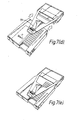
- Figures 7a, 7b and 7c are respectively top plan, side and perspective views of another embodiment of an interfacing device according to the invention. These Figures show the best mode contemplated by the inventors for putting the invention into practice.
- the device comprises, as in the embodiments described above, a case 1 of which one end 2 is intended to fit within a receiving port of a computer games console and the opposite end 3 is intended to receive an external data storage medium or memory, such as a cartridge having a read-only memory or ROM.
- the case contains, as in the embodiments described above, a printed circuit board 4 that carries interfacing circuitry, the board 4 being provided at each end thereof with suitable end connectors enabling the interfacing circuit to detachably interconnect the main processing unit of the games console and the external memory.
- a handle portion H of generally triangular construction (as viewed from above) has a concave thumb rest TR provided with ridges R.
- the external data storage medium is connectable to the interfacing device in such a manner as to be positioned underneath the handle portion H.
- Figure 7d is a perspective view showing a "game X", which can be any conventional game cartridge, about to be assembled with the device according to the invention.
- Figure 7e shows the game cartridge and the device according to the invention in assembled relation
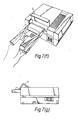
- Figure 7f shows the assembly about to be inserted into a games machine, for example a Nintendo machine.
- the assembly is conveniently grasped with the thumb of the user in the thumb rest TR and the fingers of the user below the game cartridge.
- the assembly is inserted and appears then as in Figure 7g, with the lid of the games machine resting on the thumb rest TR.
- the thumb grip prevents the game cartridge from being inserted upside down, partly because of its physical size and partly by a notch N which would catch against the lower edge of the entry port of the games machine.
- the printed circuit board 4 is thicker than normal, to allow the edge connector to make good contact (by a wedging effect) with the games machine connector without the need for the interface to be pushed down fully in the normal way. In this way, connection of the interface to the processing unit can be effected by a rectilinear movement. This enables the unit to be made smaller and more elegant.
- Mode 1 is a latch-setting mode, wherein values for the address comparison, data comparison, and data replacement functions are set by the user.
- Mode 2 is an active mode, very similar to the operation of the embodiments described above, wherein the address comparators (as well as data comparators) send a signal to a data replacement unit to effect a replacement of the data when the conditions for data replacement are met.
- the selection of modes is made over line 102 from the control latch 103.
- a CE line 92 that comes from the computer edge connector 71 is connected to the CE selector 90 which is controlled by line 102.
- the line 92 would normally connect directly to the external memory, allowing it to respond to data read/write requests from the video games machine.
- the signal on the line 92 is passed either to the external memory 93 via a CE′ line 94 or to an interface ROM 96 via a CE ⁇ line 98 depending on the state of line 102. In this way, either the external memory 93 or the interface ROM 98 is made active.
- the circuitry also has a power-on circuit 100, which ensures that the line 102 from the control latch is set to the latch setting mode when the power is first turned on.
- the purpose of this mode is to allow the user to select the address comparison data and replacement data.
- the program in the ROM 96 is designed in such a way that it will accept input from the normal game control pad, operated by the user, and use it to move an on-screen pointer around the screen. Also, on the screen there are 16 different letters (which represent values). The user can move the pointer to any of these letters and select them using a button on the game control pad. By repeating this process the user can enter this data to represent addresses, comparison data bytes and replacement data bytes, as well as function enable/disable information.
- the software stores the data entered by the user in the latches in each of the comparison/replacement units 1, 2 and 3 as well as in a control latch 103.
- the external memory has control of the CPU and the game will function normally, with the exception of any data replacement operations performed by the interface.
- the comparison/replacement units are now active, provided that the appropriate bit in the control latch has been set to enable them.
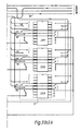
- the structure illustrated in Figures 8a, 8b and 8c includes an address bus 104 connected to comparison/replacement units 1, 2 and 3 and a data bus 105 connected to the same units.
- the address and data buses connect to the games machine, and at the right to the game cartridge that is currently in use.
- a read/write line 106 is connected to the comparison/replacement units 1, 2 and 3, to the ROM 96 and to the video games machine and the particular game cartridge in use.
- the chip enable line 92 is connected to the chip enable or CE selector 90 as described before and also the comparison/replacement units 1, 2 and 3.
- the address and data buses 104,105 are also connected to the ROM 96, and the address bus 104 is connected to a register address decoder 107.
- the latter produces four outputs which go respectively to inputs R.SEL O....3 of each of the comaprison/replacement units 1, 2 and 3.
- R.SEL O....3 inputs
- the latter input goes to a replacement data latch 0-7, a comparison data latch 0-7, a comparison address latch 0-7, and a comparison address latch 8-14.
- the data bus 105 also connects to the control latch 103, which produces the output on the line 102 to the CE selector, as noted above.
- the output on the line 102 also goes to the register address decoder 107 and to an output to Figure 8b labelled G.CONT (graphics control).
- the control latch 103 produces an output to an input labelled R.EN on each of the comparison/replacement units 1, 2 and 3 and an output to an input labelled DC.EN on each of the comparison/replacement units 1, 2 and 3.
- Each of the comparison/replacement units 1, 2 and 3 produces an output on a terminal labelled REP ("replace") which is supplied to the CE selector 90.
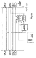
- the graphics address 0-12 bus is connected to a graphics generator 110, which produces an output to a graphic output buffer 111.
- a device selector 112 receives inputs from the G.CONT terminal and from a G CE terminal and produces outputs to the graphic output buffer 111 and the G CE terminal of the game cartridge.
- the graphics line G WE and G OE connect through Figure 8b from the games machine to the game cartridge in use.
- the replacement data latch 0-7 connects to an 8 bit buffer 115.
- An 8-bit comparator 116 receives comparison inputs from the data line DO-7 and the comparison data latch 0-7 and produces an output signal to a control 117 when the inputs are equal.
- a fifteen bit comparator 118 receives at one input an output from the comparison address latch 0-7 and an output from the comparison address latch 8-14 and at the other input data from the address line 0-14. It produces a control output to the control 117 when the inputs are equal.
- the control 117 also receives signals from the R.EN, Read/Write, chip enable, DC.EN and F.EN terminals. Its output controls the 8-bit buffer 115 and is also fed to the output terminal REP.
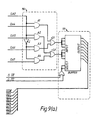
- the graphics generator 110 and the graphics output buffer 111 are shown in greater detail in Figure 9a.
- a conventional graphics generator usually generates its screen display using data read out from a graphics ROM.
- This data defines the bit patterns that form the characters/shapes to be displayed on the screen.
- the screen is divided up into a plurality of character-sized areas (squares or rectangles) - character cells - each 8x8 pixels in size.
- Each such pixel is defined by two bits in memory, representing one of four colours and the graphics ROM usually has a minimum size of 8k bytes giving 512 different character cell definitions, as would be needed for a normal game. This memory size enables the system to generate detailed, vibrant and varied displays.
- the interfacing device uses the screen for display purposes, but only to a limited extent i.e. to display sixteen letters from which the player can make a selection to set user-selectable addresses and data, and various other letters. Accordingly, the graphics generator 110 does not need to have the storage capability of a conventional graphics generator.
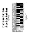
- the graphics generator 110 comprises a logic circuit which, in effect, emulates a graphics ROM containing sixteen different character cell definitions, as represented in Figure 9b.
- Figure 9a a small logic circuit is added to the circuitry needed for the rest of the device.
- the circuit of Figure 9a has a negligible cost and size, in contrast to the substantial cost and size of the separate ROM which would otherwise be required.
- the graphics generator and the graphics output buffer of Figure 9a together function as a graphics ROM emulator circuit.
- Figure 9a the graphics generator 110 and graphics buffer output 111 are of course the same as the units shown schematically in Figure 8b.
- Figure 9a shows the inputs to the graphics generator 110 on lines GA 2, GA 4, GA 5, GA 6 and GA 7 and outputs on lines GD 0, GD 1, GD 2, GD 3, GD 4, GD 5, GD 6 and GD 7 plus a select input G. OE and C.CE′.
- the graphics generator 110 includes four AND gates A1,A2,A3,A4, two OR gates 01,02 and an invertor I. If the input GA 2 is high, the OR gate 01 is high only if the input GA 4 is high and the OR gate 02 is high only if the input GA 5 is high. On the other hand, if GA 2 is low, then the OR gate 01 is high only if GA 6 is high and the OR gate 02 is high only if GA 7 is high.
- the object of the circuitry in Figure 9a is to produce the 16 character bit patterns represented in Figure 9b, these patterns being numbered respectively 0-15. Since 4 x 4 pixels are addressed as a unit, there is a sacrifice of resolution, as indicated above, but, for reasons also indicated above, it is of no particular consequence.
- a space that is not blackened corresponds to "O”
- a space that is blackened corresponds to "1".
- Figure 9c is a truth table showing the address lines in a logical order and the data values they produce to generate the 16 character cell definitions.
- FIGS. 10a, 10b and 10c when taken together form a flowchart showing the operation of the circuitry of Figures 8 and 9.
- the process moves to step 202, wherein the control latch defaults to a value which sets the CE selector 90 so as to enable the ROM 96 on line CE ⁇ 98.
- the process then moves to step 203, wherein the ROM 96 begins execution and the screen in accordance with the invention appears on the display screen on which the game is displayed.
- the program in the ROM determines whether the user has pressed a button on the control pad. If the user has not pressed such a button, the program loops back and makes the determination repeatedly until it is found that the user has pressed a button on the control pad. When the affirmative determination is made, the program moves to step 205, wherein a determination is made whether a movement button has been pressed by the user. If so, then at step 206 the program moves the cursor to a new letter and then reverts to step 204. If no movement button has been pressed, the program determines whether a fire button has been pressed by the user. If so, the program causes display of the letter under the cursor on the screen as a selected letter and then loops back to step 204. If the fire button is not found to have been pressed, the program determines at step 209 whether the start button has been pressed. If not, the program loops back to step 204.
- the program converts the selected letters (if any) to hexadecimal values which represent data to be stored in the latches.
- the program then stores hexadecimal values in latches corresponding to the addresses, data replacement values, and data compare values (if any).
- a program is transferred to the control deck's internal RAM.
- control is passed to the program in the RAM.
- the program internal memory stores a value in the control latch with the CE selector bit set so as to enable the external memory on the line CE′ 94 ( Figure 8a) and conditionally enable the replacement units and disable graphic emulation.
- control is passed to the reset address of the external memory and, at step 216, the game program begins execution.
- the device determines whether the game control is requesting a read from the external memory. If not, it loops back until an affirmative determination is made. When an affirmative determination is made, the device determines whether the value of the address bus corresponds to the address stored in one of the comparison/replacement units 1, 2 and 3. If not, the process loops back to step 217. When an affirmative determination is made, the process advances to step 219 ( Figure 10c).
- step 219 a determination is made whether the corresponding comparison/replacement function is enabled. If not, the process loops back to step 217.
- step 220 a determination is made whether the corresponding data comparison function is enabled. If it is determined that the function has been enabled, the process advances to step 221, where a determination is made whether the value of the data bus corresponds to the comparison data stored in the corresponding address/comparison unit. If no such correspondence is found, the process loops back to step 217.
- step 220 If at step 220 the corresponding data comparison function is not enabled, or if at step 221 the value of the data bus is found to correspond to the comparison data stored in the corresponding data/comparison latch, the process moves to step 222.
- the external memory is prevented from outputting data by setting the CE selector to disable the line CE′94 ( Figure 8a) via the terminal Ref.
- the corresponding comparison/replacement unit is set to output the data stored in its data replacement latch to the data bus.
- step 225 a determination is made whether the read cycle is finished. If not, the process stays in the loop at step 225 until it is determined that the read cycle is finished. When the read cycle is finished, the process advances to step 226. At step 226, the corresponding comparison/replacement unit is prevented from outputting data. Then, at step 227, the external memory is re-enabled by enabling the line CE′ 94 ( Figure 8a). The process then loops back to step 217 in Figure 10b.
- each instruction consists of two or three bytes. An explanation of the function of each instruction is given in the right-hand column.
- This section of program causes a playing unit, e.g. a plane or car, to move at a particular speed.
- ADDRESS INSTRUCTION EXPLANATION 3000 DEC 1000 This reduces the content of address 1000 by 1 (e.g. a value 28 changes to 27) 3003 BNE 300D If the value of the last step is not zero the program returns to address 3000 3005 LDA 50 This puts value 50 (from the storage location corresponding to address 3006) into a variable "A”. 3007 STA 1000 This puts the value of variable A (i.e. 50) into address 1000.
- 300A JSR "MOVE UNIT” Calls up subroutine "MOVE UNIT" which causes the unit to move.
- 300D JMP 3000 The section of the program set out above is repeated
- This section of programme causes the subroutine "MOVE UNIT" to be executed when the program steps corresponding to addresses 3000 to 3003 have been executed 50 times.
- the interfacing device sets the selected address at 3006, and sets the selected data value at 10, then the value 50, in variable "A" in the processor, (the value in the corresponding storage location of the memory) is replaced by the user-selected value (10 in this example). This would cause sub-routine "MOVE UNIT" to be executed when the program steps corresponding to addresses 3000 to 3003 have been executed 10 times instead of 50 times.
- ADDRESS INSTRUCTION EXPLANATION 2000 INC 1200 (LAP COUNT) This increments the content of address 1200 by one (increasing the lap count by one every time a player completes a lap.)
- LDA 1200 This puts the content of address 1200 into variable A (i.e. it puts the current lap count into variable "A")
- CMP 3 (LAP 3?) This compares the last value of the lap count with 3 (the value derived from the storage location corresponding to address 2005) 2006 BNE 200A If the answer is no (i.e. the comparison shows an inequality), then the program goes to 200A; otherwise it continues on.
- 2008 JMP "RACE COMPLETE” This causes a jump to the "RACE COMPLETE" part of the program.
- the number of laps required to be completed by the player is set at the value 3 derived from the addressed storage location of the memory. If, therefore, the interfacing device sets the selected address at 2005, and sets the selected data value at 7, say, then the value 3 in variable A in the processor (the value derived from the memory) is replaced by the selected value, 7 in this example.
- the described embodiments enable recognition of a single address and substitution of data corresponding thereto, the invention also embraces recognition of two or more different addresses and substitution of the respective data corresponding thereto.
- the device can alternatively be incorporated into the processing unit as an integral part thereof.
Landscapes
- Engineering & Computer Science (AREA)
- Multimedia (AREA)
- Human Computer Interaction (AREA)
- Storage Device Security (AREA)
- Stored Programmes (AREA)
- Communication Control (AREA)
- Two-Way Televisions, Distribution Of Moving Picture Or The Like (AREA)
- Telephonic Communication Services (AREA)
- Information Transfer Between Computers (AREA)
- Position Input By Displaying (AREA)
- User Interface Of Digital Computer (AREA)
- Control By Computers (AREA)
- Vehicle Body Suspensions (AREA)
- Hardware Redundancy (AREA)
Applications Claiming Priority (4)
| Application Number | Priority Date | Filing Date | Title |
|---|---|---|---|
| GB898912866A GB8912866D0 (en) | 1989-06-05 | 1989-06-05 | Interfacing device for a computer games system |
| GB8912866 | 1989-06-05 | ||
| GB8915975 | 1989-07-12 | ||
| GB898915975A GB8915975D0 (en) | 1989-06-05 | 1989-07-12 | Interfacing device for a computer games system |
Publications (3)
| Publication Number | Publication Date |
|---|---|
| EP0402067A2 true EP0402067A2 (fr) | 1990-12-12 |
| EP0402067A3 EP0402067A3 (fr) | 1992-04-29 |
| EP0402067B1 EP0402067B1 (fr) | 1997-09-10 |
Family
ID=26295440
Family Applications (1)
| Application Number | Title | Priority Date | Filing Date |
|---|---|---|---|
| EP90306034A Expired - Lifetime EP0402067B1 (fr) | 1989-06-05 | 1990-06-01 | Dispositif et méthode d'interface pour un système de jeux par ordinateur |
Country Status (8)
| Country | Link |
|---|---|
| US (1) | US5112051A (fr) |
| EP (1) | EP0402067B1 (fr) |
| JP (1) | JPH03114489A (fr) |
| AT (1) | ATE158096T1 (fr) |
| AU (1) | AU643944B2 (fr) |
| CA (1) | CA2018165C (fr) |
| DE (2) | DE69031408T2 (fr) |
| ES (1) | ES2029221T1 (fr) |
Cited By (22)
| Publication number | Priority date | Publication date | Assignee | Title |
|---|---|---|---|---|
| EP0571213A1 (fr) * | 1992-05-20 | 1993-11-24 | Codemasters Limited | Dispositif d'interface pour un système de jeux par ordinateur |
| EP0553532A3 (en) * | 1992-01-30 | 1994-03-09 | An Inc | External memory system having programmable graphics processor for use in a video game system or the like |
| EP0553531A3 (fr) * | 1992-01-30 | 1994-03-23 | An Inc | |
| US5357604A (en) * | 1992-01-30 | 1994-10-18 | A/N, Inc. | Graphics processor with enhanced memory control circuitry for use in a video game system or the like |
| EP0571138A3 (fr) * | 1992-05-20 | 1995-03-29 | Codemasters Ltd | Cartouche mémoire et interface pour console de jeu vidéo. |
| US5558339A (en) * | 1994-05-05 | 1996-09-24 | Perlman; Stephen G. | Network architecture to support recording and playback of real-time video games |
| EP0636966A3 (fr) * | 1993-07-27 | 1996-10-16 | Nintendo Co Ltd | Dispositif pour la conversion d'information d'affichage. |
| US5586257A (en) * | 1994-05-05 | 1996-12-17 | Perlman; Stephen G. | Network architecture to support multiple site real-time video games |
| US5624316A (en) * | 1994-06-06 | 1997-04-29 | Catapult Entertainment Inc. | Video game enhancer with intergral modem and smart card interface |
| US5636209A (en) * | 1994-05-05 | 1997-06-03 | Perlman; Stephen G. | Modem to support multiple site call conferenced data communications |
| US5651060A (en) * | 1994-11-15 | 1997-07-22 | Catapult Entertainment, Inc. | Method and apparatus for detecting and recovering from call waiting interruptions to modem communications |
| WO1997043020A1 (fr) * | 1996-05-14 | 1997-11-20 | Sitrick David H | Integration d'images utilisateur dans un systeme de presentation audiovisuelle et methodologie |
| US5775996A (en) * | 1994-11-14 | 1998-07-07 | Mpath Interactive, Inc. | Method and apparatus for synchronizing the execution of multiple video game systems in a networked environment |
| US5790113A (en) * | 1994-11-04 | 1998-08-04 | Catapult Entertainment | Method and apparatus for loosely sychronizing closed free-running raster displays |
| GB2326072A (en) * | 1994-04-01 | 1998-12-09 | Fujitsu Ltd | Communication unit for a game machine |
| EP0903680A3 (fr) * | 1997-09-18 | 1999-05-19 | Bung Enterprises Limited | Mémoire attachée à un support de logiciel d'un appareil de jeu par ordinateur |
| US5956485A (en) * | 1994-05-05 | 1999-09-21 | Perlman; Stephen G. | Network architecture to support real-time video games |
| US5984783A (en) * | 1994-04-01 | 1999-11-16 | Fujitsu Limited | Game machine having a communication terminal for playing games over a network service system |
| US6134590A (en) * | 1996-04-16 | 2000-10-17 | Webtv Networks, Inc. | Method and apparatus for automatically connecting devices to a local network |
| AU752025B1 (en) * | 2001-03-07 | 2002-09-05 | Igt (Australia) Pty Ltd | Method of providing secondary connections to gaming machine subsidiary interface ports |
| US7867086B2 (en) | 1992-05-22 | 2011-01-11 | Sitrick David H | Image integration with replaceable content |
| US8549403B2 (en) | 2000-11-27 | 2013-10-01 | David H. Sitrick | Image tracking and substitution system and methodology |
Families Citing this family (55)
| Publication number | Priority date | Publication date | Assignee | Title |
|---|---|---|---|---|
| GB8912866D0 (en) * | 1989-06-05 | 1989-07-26 | Code Masters Softwara | Interfacing device for a computer games system |
| GB2239810B (en) * | 1990-01-10 | 1994-06-22 | Leung Yiu Choi | Computer game control apparatus |
| JP2775334B2 (ja) * | 1990-06-22 | 1998-07-16 | 任天堂株式会社 | ゲーム装置 |
| JP2794230B2 (ja) * | 1991-07-16 | 1998-09-03 | 株式会社スクウェア | ビデオ・ゲーム装置,その制御方法および制御ディバイス |
| US5193052A (en) * | 1991-11-07 | 1993-03-09 | Advanced Matrix Technology, Inc. | Font cartridge extender with spring hook latch |
| US5203848A (en) * | 1992-01-16 | 1993-04-20 | Myson Technology, Inc. | Television game console and electronic control device for controlling the allowable playing time of the television game console |
| GB9210786D0 (en) * | 1992-05-20 | 1992-07-08 | Codemasters Ltd | Memory cartridges |
| US8821276B2 (en) | 1992-05-22 | 2014-09-02 | Bassilic Technologies Llc | Image integration, mapping and linking system and methodology |
| USD340047S (en) | 1992-09-11 | 1993-10-05 | Tseng Ching J | Card-adapter for video game |
| JP3529394B2 (ja) * | 1992-10-19 | 2004-05-24 | 株式会社東芝 | Icカード情報処理装置 |
| CA2083017C (fr) * | 1992-11-16 | 1999-02-09 | Alan Walter Ainsbury | Cartes de circuits imprimes pour montage en tandem |
| US5282621A (en) * | 1992-11-24 | 1994-02-01 | Tseng Ching J | Universal converter for non-exclusive cards of video game |
| US5362068A (en) * | 1993-04-05 | 1994-11-08 | Liu Houng Yean | Game cartridge for a television game console |
| US5470078A (en) * | 1993-11-26 | 1995-11-28 | Conlan; Tye M. | Computer controlled target shooting system |
| JP3368967B2 (ja) * | 1994-01-25 | 2003-01-20 | 任天堂株式会社 | ゲーム機用変換装置 |
| USD367895S (en) | 1994-04-11 | 1996-03-12 | Sony Corporation | Game machine |
| USD363066S (en) | 1994-06-15 | 1995-10-10 | Minnesota Mining And Manufacturing Company | Tape cartridge |
| US5451053A (en) * | 1994-09-09 | 1995-09-19 | Garrido; Fernando P. | Reconfigurable video game controller |
| US5941775A (en) * | 1994-10-14 | 1999-08-24 | Sega Of America, Inc. | Data processing system, method thereof and memory cassette |
| US6115036A (en) * | 1994-10-31 | 2000-09-05 | Nintendo Co., Ltd. | Video game/videographics program editing apparatus with program halt and data transfer features |
| US5680533A (en) * | 1994-10-31 | 1997-10-21 | Nintendo Co., Ltd. | Videographics program/video game fabricating system and method |
| US5680534A (en) * | 1994-10-31 | 1997-10-21 | Nintendo Co., Ltd. | Video game/videographics program fabricating system and method with superimpose control |
| US5599231A (en) * | 1994-10-31 | 1997-02-04 | Nintendo Co., Ltd. | Security systems and methods for a videographics and authentication game/program fabricating device |
| US5592609A (en) * | 1994-10-31 | 1997-01-07 | Nintendo Co., Ltd. | Video game/videographics program fabricating system and method with unit based program processing |
| JP3503272B2 (ja) * | 1995-05-29 | 2004-03-02 | カシオ計算機株式会社 | アダプタシステムと当該システムに用いる拡張アダプタおよび記憶装置 |
| US5768382A (en) * | 1995-11-22 | 1998-06-16 | Walker Asset Management Limited Partnership | Remote-auditing of computer generated outcomes and authenticated biling and access control system using cryptographic and other protocols |
| US5689561A (en) * | 1995-10-06 | 1997-11-18 | Pace; Michael | Computer-based trading card system and method |
| US6061656A (en) * | 1995-10-06 | 2000-05-09 | Pace; Michael | Computer-based trading card system and method |
| US8092224B2 (en) * | 1995-11-22 | 2012-01-10 | James A. Jorasch | Systems and methods for improved health care compliance |
| US20030177347A1 (en) * | 1995-11-22 | 2003-09-18 | Bruce Schneier | Methods and apparatus for awarding prizes based on authentication of computer generated outcomes using coupons |
| US7553234B2 (en) * | 1995-11-22 | 2009-06-30 | Walker Digital, Llc | Method and apparatus for outputting a result of a game via a container |
| JPH09155065A (ja) * | 1995-12-12 | 1997-06-17 | Hudson Soft Co Ltd | 特定固有データ交換可能な対戦型コンピュータゲームシステム |
| USD375090S (en) | 1996-02-12 | 1996-10-29 | Enhance Cable Technology | Video sound adaptor |
| US5947747A (en) * | 1996-05-09 | 1999-09-07 | Walker Asset Management Limited Partnership | Method and apparatus for computer-based educational testing |
| US7483670B2 (en) | 1996-05-09 | 2009-01-27 | Walker Digital, Llc | Method and apparatus for educational testing |
| JP3793313B2 (ja) * | 1997-02-18 | 2006-07-05 | 株式会社メガチップス | ゲームカセット装置 |
| US6287201B1 (en) | 1999-03-12 | 2001-09-11 | Midway Games West | Arcade game with keypad input |
| US8055509B1 (en) * | 2000-03-10 | 2011-11-08 | Walker Digital, Llc | Methods and apparatus for increasing and/or for monitoring a party's compliance with a schedule for taking medicines |
| AUPR355801A0 (en) * | 2001-03-07 | 2001-04-05 | Mikohn Gaming Australasia Pty Ltd | Method of providing secondary connections to gaming machine subsidiary interface ports |
| US20040014528A1 (en) * | 2002-07-16 | 2004-01-22 | Richard Leifer | Memory retrofit apparatus for portable game devices |
| US20050234592A1 (en) * | 2004-01-15 | 2005-10-20 | Mega Robot, Inc. | System and method for reconfiguring an autonomous robot |
| US7771280B2 (en) * | 2004-03-31 | 2010-08-10 | Nintendo Co., Ltd. | Game console connector and emulator for the game console |
| US8267780B2 (en) | 2004-03-31 | 2012-09-18 | Nintendo Co., Ltd. | Game console and memory card |
| US8016681B2 (en) * | 2004-03-31 | 2011-09-13 | Nintendo Co., Ltd. | Memory card for a game console |
| US7837558B2 (en) * | 2004-03-31 | 2010-11-23 | Nintendo Co., Ltd. | Game console and emulator for the game console |
| US11278793B2 (en) | 2004-03-31 | 2022-03-22 | Nintendo Co., Ltd. | Game console |
| US20090134181A1 (en) * | 2005-07-13 | 2009-05-28 | Vitality, Inc. | Medication dispenser with automatic refill |
| US20070016443A1 (en) * | 2005-07-13 | 2007-01-18 | Vitality, Inc. | Medication compliance systems, methods and devices with configurable and adaptable escalation engine |
| US20100328099A1 (en) * | 2005-07-13 | 2010-12-30 | Vitality, Inc. | Night Light With Embedded Cellular Modem |
| US12014328B2 (en) * | 2005-07-13 | 2024-06-18 | Vccb Holdings, Inc. | Medicine bottle cap with electronic embedded curved display |
| CN101841597A (zh) * | 2010-03-23 | 2010-09-22 | 深圳市五巨科技有限公司 | 一种控制移动终端游戏进行时间的方法和装置 |
| US9415301B2 (en) | 2013-02-26 | 2016-08-16 | Steelseries Aps | Method and apparatus for processing control signals of an accessory |
| US9295910B2 (en) | 2013-04-05 | 2016-03-29 | Hyperkin Inc. | Methods, apparatus and systems for use of a non-native chipset to play original video game cartridges |
| JP6470488B2 (ja) * | 2013-09-18 | 2019-02-13 | 任天堂株式会社 | 情報処理プログラム、情報処理装置、情報処理システム、及び情報処理方法 |
| JP7304695B2 (ja) * | 2018-12-26 | 2023-07-07 | 任天堂株式会社 | 情報処理システム、情報処理プログラム、情報処理装置、および情報処理方法 |
Family Cites Families (14)
| Publication number | Priority date | Publication date | Assignee | Title |
|---|---|---|---|---|
| US4150428A (en) * | 1974-11-18 | 1979-04-17 | Northern Electric Company Limited | Method for providing a substitute memory in a data processing system |
| JPS5721799B2 (fr) * | 1975-02-01 | 1982-05-10 | ||
| JPS5245232A (en) * | 1975-10-08 | 1977-04-09 | Hitachi Ltd | Micro program modification circuit |
| US4028678A (en) * | 1975-10-16 | 1977-06-07 | Bell Telephone Laboratories, Incorporated | Memory patching circuit |
| US4028684A (en) * | 1975-10-16 | 1977-06-07 | Bell Telephone Laboratories, Incorporated | Memory patching circuit with repatching capability |
| CA1141861A (fr) * | 1977-10-28 | 1983-02-22 | Gordon H. Smith | Microprocesseur de controle pour jeu d'adresse |
| US4218757A (en) * | 1978-06-29 | 1980-08-19 | Burroughs Corporation | Device for automatic modification of ROM contents by a system selected variable |
| US4456966A (en) * | 1981-02-26 | 1984-06-26 | International Business Machines Corporation | Memory system with flexible replacement units |
| US4432067A (en) * | 1981-05-07 | 1984-02-14 | Atari, Inc. | Memory cartridge for video game system |
| US4368515A (en) * | 1981-05-07 | 1983-01-11 | Atari, Inc. | Bank switchable memory system |
| GB2118809B (en) * | 1982-01-11 | 1986-07-30 | Atari Inc | Self-adjusting game difficulty method and apparatus for electronic games |
| US4480835A (en) * | 1983-03-02 | 1984-11-06 | Williams Theodore R | Cartridge adapter for programmable video games |
| JPH07100088B2 (ja) * | 1986-11-07 | 1995-11-01 | 任天堂株式会社 | ゲ−ム機用カ−トリツジのアダプタ |
| CA1330596C (fr) * | 1986-11-19 | 1994-07-05 | Yoshiaki Nakanishi | Cartouche de memoire et appareil de traitement de donnees |
-
1990
- 1990-05-30 US US07/530,617 patent/US5112051A/en not_active Ceased
- 1990-06-01 DE DE69031408T patent/DE69031408T2/de not_active Expired - Fee Related
- 1990-06-01 ES ES199090306034T patent/ES2029221T1/es active Pending
- 1990-06-01 EP EP90306034A patent/EP0402067B1/fr not_active Expired - Lifetime
- 1990-06-01 DE DE199090306034T patent/DE402067T1/de active Pending
- 1990-06-01 AT AT90306034T patent/ATE158096T1/de not_active IP Right Cessation
- 1990-06-04 CA CA002018165A patent/CA2018165C/fr not_active Expired - Fee Related
- 1990-06-05 JP JP2147188A patent/JPH03114489A/ja active Pending
- 1990-06-05 AU AU56287/90A patent/AU643944B2/en not_active Ceased
Cited By (36)
| Publication number | Priority date | Publication date | Assignee | Title |
|---|---|---|---|---|
| EP1262921A3 (fr) * | 1992-01-30 | 2004-03-24 | A/N Inc. | Système de mémoire externe avec processeur graphique programmable pour utilisation dans un système de jeu vidéo ou similaire |
| US6646653B2 (en) | 1992-01-30 | 2003-11-11 | A/N Inc. | Programmable graphics processor for use in a video game system or the like |
| EP0553531A3 (fr) * | 1992-01-30 | 1994-03-23 | An Inc | |
| US5357604A (en) * | 1992-01-30 | 1994-10-18 | A/N, Inc. | Graphics processor with enhanced memory control circuitry for use in a video game system or the like |
| US5388841A (en) * | 1992-01-30 | 1995-02-14 | A/N Inc. | External memory system having programmable graphics processor for use in a video game system or the like |
| US5850230A (en) * | 1992-01-30 | 1998-12-15 | A/N Inc. | External memory system having programmable graphics processor for use in a video game system or the like |
| US5724497A (en) * | 1992-01-30 | 1998-03-03 | A/N Inc. | Programmable graphics processor having pixel to character conversion hardware for use in a video game system or the like |
| US7229355B2 (en) | 1992-01-30 | 2007-06-12 | Nintendo Co., Ltd. | External memory system having programmable graphics processor for use in a video game system of the like |
| EP0553532A3 (en) * | 1992-01-30 | 1994-03-09 | An Inc | External memory system having programmable graphics processor for use in a video game system or the like |
| US7432932B2 (en) | 1992-01-30 | 2008-10-07 | Nintendo Co., Ltd. | External memory system having programmable graphics processor for use in a video game system or the like |
| US5599232A (en) * | 1992-05-02 | 1997-02-04 | Codemasters Limited | Memory cartridge with interface having graphics co-processor |
| EP0571213A1 (fr) * | 1992-05-20 | 1993-11-24 | Codemasters Limited | Dispositif d'interface pour un système de jeux par ordinateur |
| EP0571138A3 (fr) * | 1992-05-20 | 1995-03-29 | Codemasters Ltd | Cartouche mémoire et interface pour console de jeu vidéo. |
| US7867086B2 (en) | 1992-05-22 | 2011-01-11 | Sitrick David H | Image integration with replaceable content |
| US8317611B2 (en) | 1992-05-22 | 2012-11-27 | Bassilic Technologies Llc | Image integration, mapping and linking system and methodology |
| US6425825B1 (en) | 1992-05-22 | 2002-07-30 | David H. Sitrick | User image integration and tracking for an audiovisual presentation system and methodology |
| US5830065A (en) * | 1992-05-22 | 1998-11-03 | Sitrick; David H. | User image integration into audiovisual presentation system and methodology |
| EP0636966A3 (fr) * | 1993-07-27 | 1996-10-16 | Nintendo Co Ltd | Dispositif pour la conversion d'information d'affichage. |
| GB2326072A (en) * | 1994-04-01 | 1998-12-09 | Fujitsu Ltd | Communication unit for a game machine |
| GB2326072B (en) * | 1994-04-01 | 1999-02-10 | Fujitsu Ltd | Communication unit for game machine |
| US5984783A (en) * | 1994-04-01 | 1999-11-16 | Fujitsu Limited | Game machine having a communication terminal for playing games over a network service system |
| US5636209A (en) * | 1994-05-05 | 1997-06-03 | Perlman; Stephen G. | Modem to support multiple site call conferenced data communications |
| US5558339A (en) * | 1994-05-05 | 1996-09-24 | Perlman; Stephen G. | Network architecture to support recording and playback of real-time video games |
| US5956485A (en) * | 1994-05-05 | 1999-09-21 | Perlman; Stephen G. | Network architecture to support real-time video games |
| US6026079A (en) * | 1994-05-05 | 2000-02-15 | Webtv Networks, Inc. | Modem to support multiple site call conferenced data communications |
| US5586257A (en) * | 1994-05-05 | 1996-12-17 | Perlman; Stephen G. | Network architecture to support multiple site real-time video games |
| US5624316A (en) * | 1994-06-06 | 1997-04-29 | Catapult Entertainment Inc. | Video game enhancer with intergral modem and smart card interface |
| US5790113A (en) * | 1994-11-04 | 1998-08-04 | Catapult Entertainment | Method and apparatus for loosely sychronizing closed free-running raster displays |
| US5775996A (en) * | 1994-11-14 | 1998-07-07 | Mpath Interactive, Inc. | Method and apparatus for synchronizing the execution of multiple video game systems in a networked environment |
| US5651060A (en) * | 1994-11-15 | 1997-07-22 | Catapult Entertainment, Inc. | Method and apparatus for detecting and recovering from call waiting interruptions to modem communications |
| US6134590A (en) * | 1996-04-16 | 2000-10-17 | Webtv Networks, Inc. | Method and apparatus for automatically connecting devices to a local network |
| WO1997043020A1 (fr) * | 1996-05-14 | 1997-11-20 | Sitrick David H | Integration d'images utilisateur dans un systeme de presentation audiovisuelle et methodologie |
| EP0903680A3 (fr) * | 1997-09-18 | 1999-05-19 | Bung Enterprises Limited | Mémoire attachée à un support de logiciel d'un appareil de jeu par ordinateur |
| US8549403B2 (en) | 2000-11-27 | 2013-10-01 | David H. Sitrick | Image tracking and substitution system and methodology |
| US9135954B2 (en) | 2000-11-27 | 2015-09-15 | Bassilic Technologies Llc | Image tracking and substitution system and methodology for audio-visual presentations |
| AU752025B1 (en) * | 2001-03-07 | 2002-09-05 | Igt (Australia) Pty Ltd | Method of providing secondary connections to gaming machine subsidiary interface ports |
Also Published As
| Publication number | Publication date |
|---|---|
| EP0402067A3 (fr) | 1992-04-29 |
| AU5628790A (en) | 1990-12-06 |
| JPH03114489A (ja) | 1991-05-15 |
| EP0402067B1 (fr) | 1997-09-10 |
| DE69031408T2 (de) | 1998-03-05 |
| ATE158096T1 (de) | 1997-09-15 |
| US5112051A (en) | 1992-05-12 |
| DE69031408D1 (de) | 1997-10-16 |
| DE402067T1 (de) | 1992-06-11 |
| ES2029221T1 (es) | 1992-08-01 |
| AU643944B2 (en) | 1993-12-02 |
| CA2018165C (fr) | 1999-02-16 |
| CA2018165A1 (fr) | 1990-12-05 |
Similar Documents
| Publication | Publication Date | Title |
|---|---|---|
| EP0402067B1 (fr) | Dispositif et méthode d'interface pour un système de jeux par ordinateur | |
| USRE35520E (en) | Interfacing device for a computer games system | |
| KR0148364B1 (ko) | 비인정 외부 메모리 사용방지를 위한 시스템 | |
| US5184830A (en) | Compact hand-held video game system | |
| US4156928A (en) | Programmable television game and training system with adaptable operator control | |
| US6676520B2 (en) | Video game system providing physical sensation | |
| US4672541A (en) | Video game with interactive enlarged play action inserts | |
| US6315669B1 (en) | Portable color display game machine and storage medium for the same | |
| US5265888A (en) | Game apparatus and memory cartridge used therefor | |
| US4976435A (en) | Video game control adapter | |
| US7052397B2 (en) | Entertainment system, recording medium and entertainment apparatus | |
| US5802544A (en) | Addressing multiple removable memory modules by remapping slot addresses | |
| EP0431723A2 (fr) | Machine de jeu de télévision | |
| US5356156A (en) | Game apparatus and method of playing a game | |
| US6241610B1 (en) | Three-dimensional image processing system having dynamically changing character polygon number | |
| USRE36675E (en) | Game apparatus and memory cartridge used therefor | |
| CA2045072C (fr) | Appareil de jeu et cartouche de memoire connexe | |
| AU671132B2 (en) | A game machine | |
| US4618146A (en) | Video game apparatus allowing for a variation in playing sequence | |
| US20010053716A1 (en) | Game character generating method, storage medium and video game device | |
| JPH10314453A (ja) | ゲーム装置、ゲーム表示方法及び記録媒体 | |
| JPH09218721A (ja) | 画像処理用拡張装置および拡張装置を用いた画像処理システム | |
| JP3857894B2 (ja) | ビデオゲーム装置の入力制御方法及びその方法を実行するためのコンピュータプログラム | |
| KR950007343Y1 (ko) | 조이스틱 게임의 자동실행회로 | |
| Scrimshaw et al. | Real-Time Graphics |
Legal Events
| Date | Code | Title | Description |
|---|---|---|---|
| PUAI | Public reference made under article 153(3) epc to a published international application that has entered the european phase |
Free format text: ORIGINAL CODE: 0009012 |
|
| AK | Designated contracting states |
Kind code of ref document: A2 Designated state(s): AT BE CH DE DK ES FR GB GR IT LI LU NL SE |
|
| PUAL | Search report despatched |
Free format text: ORIGINAL CODE: 0009013 |
|
| ITCL | It: translation for ep claims filed |
Representative=s name: UFFICIO TECNICO ING. A. MANNUCCI |
|
| EL | Fr: translation of claims filed | ||
| AK | Designated contracting states |
Kind code of ref document: A3 Designated state(s): AT BE CH DE DK ES FR GB GR IT LI LU NL SE |
|
| 17P | Request for examination filed |
Effective date: 19920406 |
|
| DET | De: translation of patent claims | ||
| REG | Reference to a national code |
Ref country code: ES Ref legal event code: BA2A Ref document number: 2029221 Country of ref document: ES Kind code of ref document: T1 |
|
| RAP1 | Party data changed (applicant data changed or rights of an application transferred) |
Owner name: CODEMASTERS LIMITED |
|
| 17Q | First examination report despatched |
Effective date: 19930312 |
|
| REG | Reference to a national code |
Ref country code: DE Ref legal event code: 8580 Free format text: DER ANMELDER LAUTET RICHTIG: CODEMASTERS LTD., LONDON, GB |
|
| GRAG | Despatch of communication of intention to grant |
Free format text: ORIGINAL CODE: EPIDOS AGRA |
|
| GRAH | Despatch of communication of intention to grant a patent |
Free format text: ORIGINAL CODE: EPIDOS IGRA |
|
| GRAH | Despatch of communication of intention to grant a patent |
Free format text: ORIGINAL CODE: EPIDOS IGRA |
|
| RAP1 | Party data changed (applicant data changed or rights of an application transferred) |
Owner name: CODEMASTERS LIMITED |
|
| GRAA | (expected) grant |
Free format text: ORIGINAL CODE: 0009210 |
|
| AK | Designated contracting states |
Kind code of ref document: B1 Designated state(s): AT BE CH DE DK ES FR GB GR IT LI LU NL SE |
|
| PG25 | Lapsed in a contracting state [announced via postgrant information from national office to epo] |
Ref country code: IT Free format text: LAPSE BECAUSE OF FAILURE TO SUBMIT A TRANSLATION OF THE DESCRIPTION OR TO PAY THE FEE WITHIN THE PRE;WARNING: LAPSES OF ITALIAN PATENTS WITH EFFECTIVE DATE BEFORE 2007 MAY HAVE OCCURRED AT ANY TIME BEFORE 2007. THE CORRECT EFFECTIVE DATE MAY BE DIFFERENT FROM THE ONE RECORDED.SCRIBED TIME-LIMIT Effective date: 19970910 Ref country code: BE Effective date: 19970910 Ref country code: GR Free format text: LAPSE BECAUSE OF FAILURE TO SUBMIT A TRANSLATION OF THE DESCRIPTION OR TO PAY THE FEE WITHIN THE PRESCRIBED TIME-LIMIT Effective date: 19970910 Ref country code: NL Free format text: LAPSE BECAUSE OF FAILURE TO SUBMIT A TRANSLATION OF THE DESCRIPTION OR TO PAY THE FEE WITHIN THE PRESCRIBED TIME-LIMIT Effective date: 19970910 Ref country code: DK Free format text: LAPSE BECAUSE OF NON-PAYMENT OF DUE FEES Effective date: 19970910 Ref country code: AT Effective date: 19970910 Ref country code: LI Free format text: LAPSE BECAUSE OF FAILURE TO SUBMIT A TRANSLATION OF THE DESCRIPTION OR TO PAY THE FEE WITHIN THE PRESCRIBED TIME-LIMIT Effective date: 19970910 Ref country code: CH Free format text: LAPSE BECAUSE OF FAILURE TO SUBMIT A TRANSLATION OF THE DESCRIPTION OR TO PAY THE FEE WITHIN THE PRESCRIBED TIME-LIMIT Effective date: 19970910 |
|
| REF | Corresponds to: |
Ref document number: 158096 Country of ref document: AT Date of ref document: 19970915 Kind code of ref document: T |
|
| REG | Reference to a national code |
Ref country code: CH Ref legal event code: EP |
|
| REF | Corresponds to: |
Ref document number: 69031408 Country of ref document: DE Date of ref document: 19971016 |
|
| PG25 | Lapsed in a contracting state [announced via postgrant information from national office to epo] |
Ref country code: SE Effective date: 19971210 |
|
| ET | Fr: translation filed | ||
| NLV1 | Nl: lapsed or annulled due to failure to fulfill the requirements of art. 29p and 29m of the patents act | ||
| REG | Reference to a national code |
Ref country code: CH Ref legal event code: PL |
|
| PG25 | Lapsed in a contracting state [announced via postgrant information from national office to epo] |
Ref country code: ES Free format text: LAPSE BECAUSE OF FAILURE TO SUBMIT A TRANSLATION OF THE DESCRIPTION OR TO PAY THE FEE WITHIN THE PRESCRIBED TIME-LIMIT Effective date: 19980325 |
|
| PG25 | Lapsed in a contracting state [announced via postgrant information from national office to epo] |
Ref country code: LU Free format text: LAPSE BECAUSE OF NON-PAYMENT OF DUE FEES Effective date: 19980601 |
|
| PLBE | No opposition filed within time limit |
Free format text: ORIGINAL CODE: 0009261 |
|
| STAA | Information on the status of an ep patent application or granted ep patent |
Free format text: STATUS: NO OPPOSITION FILED WITHIN TIME LIMIT |
|
| 26N | No opposition filed | ||
| REG | Reference to a national code |
Ref country code: GB Ref legal event code: IF02 |
|
| PGFP | Annual fee paid to national office [announced via postgrant information from national office to epo] |
Ref country code: GB Payment date: 20020529 Year of fee payment: 13 |
|
| PGFP | Annual fee paid to national office [announced via postgrant information from national office to epo] |
Ref country code: FR Payment date: 20020610 Year of fee payment: 13 Ref country code: DE Payment date: 20020610 Year of fee payment: 13 |
|
| PG25 | Lapsed in a contracting state [announced via postgrant information from national office to epo] |
Ref country code: GB Free format text: LAPSE BECAUSE OF NON-PAYMENT OF DUE FEES Effective date: 20030601 |
|
| PG25 | Lapsed in a contracting state [announced via postgrant information from national office to epo] |
Ref country code: DE Free format text: LAPSE BECAUSE OF NON-PAYMENT OF DUE FEES Effective date: 20040101 |
|
| GBPC | Gb: european patent ceased through non-payment of renewal fee |
Effective date: 20030601 |
|
| PG25 | Lapsed in a contracting state [announced via postgrant information from national office to epo] |
Ref country code: FR Free format text: LAPSE BECAUSE OF NON-PAYMENT OF DUE FEES Effective date: 20040227 |
|
| REG | Reference to a national code |
Ref country code: FR Ref legal event code: ST |